Deterministic reflection contrast ellipsometry for thick multilayer two-dimensional heterostructures
-
Kang Ryeol Lee
 ,
JinGyu Youn
,
JinGyu Youn


Abstract
Optical spectroscopy is a powerful tool for characterizing the properties of two-dimensional (2D) heterostructures. However, extracting the permittivity information of each 2D layer in optically thick heterostructures is challenging because of interference. To accurately measure the optical permittivity of each 2D layer in a heterostructure or on a substrate with a thick insulating spacer, such as oxides, we propose deterministic reflection contrast ellipsometry (DRCE). Our DRCE method has two advantages over conventional techniques. It deterministically measures the optical permittivity of 2D materials using only the measured reflection spectra of the heterostructure, rather than dispersion fitting as in spectroscopic ellipsometry. Additionally, the DRCE is free of excitonic energy errors in reflection-contrast spectroscopy. We believe that DRCE will enable accurate and rapid characterization of 2D materials.
1 Introduction
A vertical stack of few-atom-thick two-dimensional (2D) materials, known as a 2D heterostructure, has unique properties, such as Moire excitons [1], Wigner crystal states [2], and superconductivity [3], that are not present in the 2D layers of ingredients or their three-dimensional bulk counterparts [4–13]. Optical spectroscopy has been widely used to characterize the properties of 2D heterostructures because it is versatile, noninvasive, and usually requires simple optical components [14]. Stimulated by the huge interest in 2D heterostructures, various optical spectroscopic techniques have been proposed to measure the optical permittivity, a parameter describing the optical response of 2D materials [15], [16], [17], [18], [19], [20], [21]. Spectroscopic ellipsometry (SE) and reflection contrast (RC) spectroscopy are the most common techniques; however, they have inherent drawbacks in the accurate characterization of 2D materials in optically thick 2D heterostructures, whose interference effect is prominent [14].
SE is a common method for determining the permittivity of a general material [22]. SE measures the change in polarization upon reflection and calculates the optical permittivity that reproduces the experimentally measured spectra using a least-squares fit for the known dispersion models [18]. However, prior knowledge of the electronic structure of the 2D material sample outside the spectral region of interest is required [14], [18], [20]; for example, in the monolayer transition metal dichalcogenides (TMDs), electronic transitions in the ultraviolet frequency region can affect the optical permittivity in the visible frequency region [14], [18], [20]. Because of this limitation, determining the optical permittivity of a 2D material sample using only the measured reflection spectra is difficult.
However, RC spectroscopy is the most prevalent deterministic approach for characterizing 2D materials owing to its simple experimental implementation and deterministic measurement properties [18]. RC spectroscopy measures the reflectance R of a 2D sample and its substrate at a normal angle of incidence, and their difference directly indicates the absorption of the 2D sample, that is, the imaginary part of the permittivity, in a deterministic manner [14]. However, RC spectroscopy has two drawbacks: (i) RC spectroscopy measures only the imaginary part of the permittivity if the substrate is nonabsorptive, whereas the real part cannot be obtained directly from the measured spectra. (ii) RC spectroscopy fails when the effects of multiple reflections play an important role in thick optical systems or when the substrate is absorptive [14]. For example, the imaginary part of the permittivity of a 2D material is measured inaccurately when its substrate has an oxide spacer, for example, a SiO2/Si substrate, which is typically used to enhance the visibility of atomically thin 2D materials [23], [24], [25], [26], [27], [28], [29]. This drawback of RC spectroscopy is critical for the accuracy of the exciton energy in the permittivity measurement of 2D semiconductors, for example, TMDs, as shown in Figure 1(b). Therefore, RC spectroscopy cannot be applied to thick multilayer 2D heterostructures.
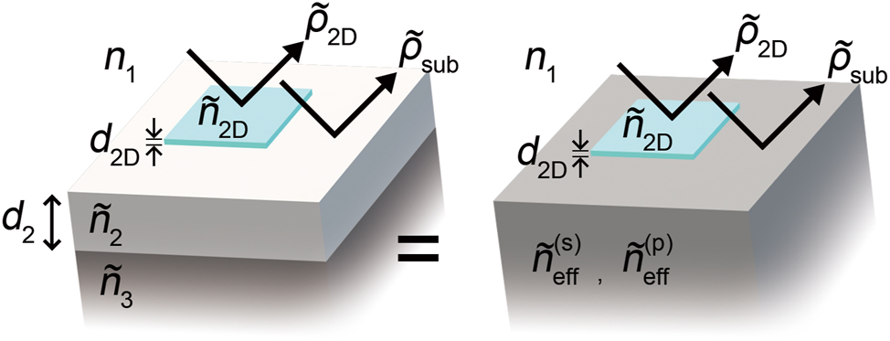
The schematic drawing of DRCE. DRCE characterizes the refractive index of the topmost 2D layer (
In this study, we propose deterministic reflection contrast ellipsometry (DRCE) to measure the optical permittivity of 2D material layers in an optically thick heterostructure. DRCE measures the changes in polarization upon reflection at each interface in an optically thick heterostructure and algorithmically determines the permittivity using only the measured spectra of the polarization changes. The experimental implementation of the DRCE is also straightforward because it requires simple optics for reflection measurement at an oblique angle of incidence with a few polarization gadgets, such as polarizers and polarization compensators. We theoretically and experimentally demonstrated the validity of a DRCE using 2D TMDs, including monolayer MoS2 and WSe2 on a Si substrate with a thick SiO2 spacer. Our proposed DRCE technique can promote experimental efforts to discover new physics in 2D heterostructures and develop 2D optoelectronic applications.
2 Results
2.1 Summary of our approach
Figure 1 shows the concept of DRCE. DRCE aims to measure the complex refractive index
Using the effective substrate reduction, any optically thick multilayer can be replaced with a single substrate. This enables analytic determination of the index of the topmost layer on the multilayer. DRCE measurement combines conventional ellipsometry and RC spectroscopy. As in conventional ellipsometry, DRCE measures the complex reflection ratio
2.2 Effective substrate reduction
The proposed DRCE method is based on effective substrate reduction; light reflection by a single layer on a substrate is equivalent to that of a reduced substrate whose effective refractive index
This equivalence allows the reduction of a N layer system to a (N − 1) layer system if we know all the s-wave (
![Figure 2:
Two experimental schemes for deterministic reflection contrast ellipsometry (DRCE): (a) Scheme I: A staircase multilayer structure; reflection ratio (
ρ
̃
$\tilde {\rho }$
) measurements are performed at the interface of each layer and air. (b) Scheme II: A general multilayer structure; reflection ratio measurements are performed before the next layer preparation. (c) Schematic drawing of the subsequent effective substrate reduction for DRCE. (d) Reflection contrast (RC) spectra δR of monolayer MoS2 on the SiO2/Si substrate is plotted as a function of oxide thickness. Exciton energies are depicted in the black dashed line in the magnified inset. Apparent peaks in RC spectra are shifted as oxide thickness varies, resulting in inaccurate measurement of exciton energies using RC spectroscopy. (e) The complex refractive index
n
̃
=
n
+
i
k
$\tilde {n}=n+ik$
of the same monolayer MoS2 on the SiO2/Si substrate characterized by DRCE at the angle of incidence of 40°. The reference refractive index is obtained from the literature [20], and it is plotted in the left and right sides of the plots. Exciton energies are not shifted in our method although some errors in their magnitudes depend on the oxide thickness. Figure 1(d) and (e) show theoretical calculations.](/document/doi/10.1515/nanoph-2023-0753/asset/graphic/j_nanoph-2023-0753_fig_002.jpg)
Two experimental schemes for deterministic reflection contrast ellipsometry (DRCE): (a) Scheme I: A staircase multilayer structure; reflection ratio (
Subsequent reduction of the effective substrate yielded a single top layer on the reduced substrate (Figure 2(c)). This suggests that the complicated ellipsometry problem for the N-layer system can always be reduced to a simple RC ellipsometry problem for a single-layer system if we can measure the reflections of the s-wave (
Analytically, the effective refractive indices of the reduced substrate replacing the single layer and its substrate are expressed as follows (see Supplementary Materials for details on the derivation),
for the p- and s-polarizations of light, respectively. Notations in Eqs. (1) and (2) follow Figure 1. Plus-minus sign in Eq. (1) can be determined by continuous and nonvanishing values in
where
2.3 Deterministic reflection contrast ellipsometry (DRCE)
By the effective substrate reduction, any multilayer system can be reduced to the reduced substrate whose effective indices are given by Eqs. (1) and (2). Let a 2D material layer of index
where the functions A, B, and α are defined as follows:
where λ is the wavelength of light. Notations in Eqs. (4)–(7) follow Figure 1. Eq. (4) is a key result of this study. Note that n
1 is the index of the superstrate in Eqs. (4)–(7). All variables in Eqs. (4)–(7), except for the experimentally measured δ, are known for a given sample. It is also noteworthy that Eq. (4) is obtained by the first-order expansion of δ in a function of the optical path length
In DRCE, the angle of incidence should be carefully chosen because Eq. (4) is singular if
2.4 Experiment and simulation results
To verify the permittivity characterization using Eq. (4) for a given reflection-ratio contrast δ, we theoretically simulated the DRCE of monolayer MoS2 on a SiO2/Si substrate with an oxide thickness of 280 nm. In our previous study, we calculated the reflection ratio contrast δ using the transfer matrix technique [32] and tabulated the permittivity of monolayer MoS2. We use the monolayer thickness d
2D = 0.65 nm in the following [20]. As illustrated in Figure 3, we compare the permittivity obtained by DRCE at various angles of incidence (color profiles) with the reference permittivity [20] (insets on the left and right sides). First, we identified that the positions of the excitonic peaks remained nearly constant and were the same as the reference permittivity for all angles of incidence. Second, the DRCE results for the permittivity became more accurate over a broad energy range as the angle of incidence increased. To quantify the accuracy of DRCE, we plot its error, (
![Figure 3:
Simulation for the DRCE measurement of the refractive index of monolayer MoS_2: (a) Refractive index
n
̃
=
n
+
i
k
$\tilde {n}=n+ik$
of monolayer MoS2 characterized by DRCE with different angles of incidence. Monolayer MoS2 is sitting on the SiO2/Si substrate with oxide thickness of 280 nm. The real (n
ref
) and imaginary parts (k
ref
) of the reference refractive index [20] (
n
̃
ref
=
n
ref
+
i
k
ref
${\tilde {n}}_{\mathit{ref}}={n}_{\mathit{ref}}+i{k}_{\mathit{ref}}$
) are plotted in the left and right sides, respectively. Exciton energies are displayed by black arrows. (b) Corresponding errors of DRCE for the refractive index (
δ
n
ref
=
n
ref
−
n
/
n
ref
$\delta {n}_{\mathit{ref}}=\left({n}_{\mathit{ref}}-n\right)/{n}_{\mathit{ref}}$
and
δ
k
ref
=
k
ref
−
k
/
k
ref
$\delta {k}_{\mathit{ref}}=\left({k}_{\mathit{ref}}-k\right)/{k}_{\mathit{ref}}$
). Black lines in (b) are destructive interference condition of the oxide layer.](/document/doi/10.1515/nanoph-2023-0753/asset/graphic/j_nanoph-2023-0753_fig_003.jpg)
Simulation for the DRCE measurement of the refractive index of monolayer MoS_2: (a) Refractive index
In addition, we simulated the DRCE of a 2D heterostructure composed of a monolayer MoS2/monolayer WSe2/280 nm-thick SiO2/Si substrate in Figure 4. The refractive index of each monolayer TMDs can be obtained sequentially by the reflection ratio contrast δ at each layer/air interface. (i) Using the reflection ratio contrast δ between the SiO2 layer and the substrate, oxide layer and substrate are replaced with the first reduced substrate. (ii) Using the reflection ratio contrast δ between the monolayer WSe2 and SiO2/Si substrate (i.e., the first reduced substrate), we can obtain the refractive index of the monolayer WSe2 using Eq. (4). Moreover, the reflection ratio contrast δ yields the second reduced substrate. (iii) Finally, using the reflection ratio contrast δ between monolayer MoS2 and the monolayer WSe2/SiO2/Si substrate (i.e., the second reduced substrate), we can obtain the refractive index of the monolayer MoS2 by Eq. (4). This procedure is illustrated in Figure 2(a). Figure 4(a) and (b) show the refractive indices of the two monolayers at an incident angle of 50°. As mentioned in the discussion of Figure 3, the errors are prominent in the short-wavelength region (i.e., the high-energy region). In the long-wavelength region, the refractive index can be accurately measured using the DRCE. We also performed DRCE measurements at higher angles (Figure S2 in the Supplementary Material). Higher angle measurements show that the error region moves to the shorter wavelengths, as also shown in Figure 3(b). We emphasize that multilayered 2D heterostructures with more than two layers can be characterized in the same manner, that is, the subsequent reduction of the reduced substrate and DRCE.
![Figure 4:
DRCE characterization of the refractive index of each 2D monolayer TMD in the heterostructure composed of monolayer MoS2/monolayer WSe2/280 nm-thick SiO2/Si substrate. (a) The real (n) and (b) imaginary parts (k) of the refractive index (the orange solid line: DRCE result of monolayer MoS2, the green solid line: DRCE result of monolayer WSe2, the red dashed line: reference value for of monolayer MoS2, and blue dashed line: reference value for of monolayer WSe2). In Figure 3, the angle of incidence is fixed at 50°. Reference refractive indices of monolayer MoS2 and WSe2 are obtained from our previous study [20].](/document/doi/10.1515/nanoph-2023-0753/asset/graphic/j_nanoph-2023-0753_fig_004.jpg)
DRCE characterization of the refractive index of each 2D monolayer TMD in the heterostructure composed of monolayer MoS2/monolayer WSe2/280 nm-thick SiO2/Si substrate. (a) The real (n) and (b) imaginary parts (k) of the refractive index (the orange solid line: DRCE result of monolayer MoS2, the green solid line: DRCE result of monolayer WSe2, the red dashed line: reference value for of monolayer MoS2, and blue dashed line: reference value for of monolayer WSe2). In Figure 3, the angle of incidence is fixed at 50°. Reference refractive indices of monolayer MoS2 and WSe2 are obtained from our previous study [20].
In Figure 5, we performed a DRCE experiment on a chemical vapor deposition (CVD)-grown monolayer MoS2 on a SiO2/Si substrate with an oxide thickness of 280 nm (purchased from SixCarbon), which has the same structure as the theoretical simulation of DECR shown in Figure 3. The reflection ratio
![Figure 5:
DRCE experiment for monolayer MoS2 in the heterostructure composed of CVD-grown monolayer MoS2/280 nm-thick SiO2/Si substrate. (a) The real (n) and (b) imaginary parts (k) of refractive index characterized at the incident angle of 40°. (The solid orange line: DRCE experiment results, the dashed red line: DRCE theoretical simulation results, and the dashed blue line: reference refractive index of monolayer MoS2 obtained from our previous study [20]).](/document/doi/10.1515/nanoph-2023-0753/asset/graphic/j_nanoph-2023-0753_fig_005.jpg)
DRCE experiment for monolayer MoS2 in the heterostructure composed of CVD-grown monolayer MoS2/280 nm-thick SiO2/Si substrate. (a) The real (n) and (b) imaginary parts (k) of refractive index characterized at the incident angle of 40°. (The solid orange line: DRCE experiment results, the dashed red line: DRCE theoretical simulation results, and the dashed blue line: reference refractive index of monolayer MoS2 obtained from our previous study [20]).
3 Conclusions
We addressed the issues in conventional optical techniques, such as RC spectroscopy and SE, to characterize the permittivity of 2D material layers in optically thick heterostructures. The conventional techniques had some limitations, such as (i) nondeterministic permittivity measurements requiring dispersion fitting (in SE [18]), (ii) partial measurement of the imaginary part of the permittivity (in RC spectroscopy [16]), and (iii) measurement failure on the substrate with a thick oxide spacer layer (in RC spectroscopy and our previous study [20]). We demonstrated that DRCE is free from such limitations in determining the permittivity of each 2D material layer in the heterostructure (see Figure S3 for example to compare our method to conventional methods). We also note that our method can be applied to transparent 2D materials such as graphene and hBN (Figure S4). Our method may enable the rapid and noninvasive optical characterization of 2D material layers in thick heterostructures.
Funding source: National Research Foundation of Korea
Award Identifier / Grant number: 2022R1F1A1074019
Award Identifier / Grant number: RS-2023-00254920
-
Research funding: This work was supported by the National Research Foundation of Korea (NRF) grant funded by the Korea government (MSIT) (No. RS-2023-00254920, No. 2022R1F1A1074019).
-
Author contributions: All authors have accepted responsibility for the entire content of this manuscript and approved its submission. All authors have given approval to the final version of the manuscript. K.L and S.Y. wrote the manuscript. S.Y. conceived the project. K.L. and S.Y. derived equations for DRCE. K.L. performed the ellipsometry experiments. K.L. and J.Y. performed numerical calculations using the transfer matrix technique.
-
Conflict of interest: Authors state no conflicts of interest.
-
Informed consent: Informed consent was obtained from all individuals included in this study.
-
Ethical approval: The conducted research is not related to either human or animals use.
-
Data availability: All data generated or analyzed during this study are included in this published article and its supplementary information files.
References
[1] C. Jin, et al.., “Observation of moiré excitons in WSe2/WS2 heterostructure superlattices,” Nature, vol. 567, no. 7746, pp. 76–80, 2019. https://doi.org/10.1038/s41586-019-0976-y.Suche in Google Scholar PubMed
[2] E. C. Regan, et al.., “Mott and generalized Wigner crystal states in WSe2/WS2 moiré superlattices,” Nature, vol. 579, no. 7799, pp. 359–363, 2020. https://doi.org/10.1038/s41586-020-2092-4.Suche in Google Scholar PubMed
[3] G. Chen, et al.., “Signatures of tunable superconductivity in a trilayer graphene moiré superlattice,” Nature, vol. 572, no. 7768, pp. 215–219, 2019. https://doi.org/10.1038/s41586-019-1393-y.Suche in Google Scholar PubMed
[4] M. Y. Li, C. H. Chen, Y. Shi, and L. J. Li, “Heterostructures based on two-dimensional layered materials and their potential applications,” Mater. Today, vol. 19, no. 6, pp. 322–335, 2016. https://doi.org/10.1016/j.mattod.2015.11.003.Suche in Google Scholar
[5] P. V. Pham, et al.., “2D heterostructures for ubiquitous electronics and optoelectronics: principles, opportunities, and challenges,” Chem. Rev., vol. 122, no. 6, pp. 6514–6613, 2022. https://doi.org/10.1021/acs.chemrev.1c00735.Suche in Google Scholar PubMed
[6] S. Wang, et al.., “Gate-tunable plasmons in mixed-dimensional van der Waals heterostructures,” Nat. Commun., vol. 12, no. 1, p. 5039, 2021. https://doi.org/10.1038/s41467-021-25269-0.Suche in Google Scholar PubMed PubMed Central
[7] P. Nagler, et al.., “Giant magnetic splitting inducing near-unity valley polarization in van der Waals heterostructures,” Nat. Commun., vol. 8, no. 1, pp. 1551–1556, 2017. https://doi.org/10.1038/s41467-017-01748-1.Suche in Google Scholar PubMed PubMed Central
[8] C. Jin, et al.., “Imaging of pure spin-valley diffusion current in WS 2-WSe 2 heterostructures,” Science, vol. 360, no. 6391, pp. 893–896, 2018. https://doi.org/10.1126/science.aao3503.Suche in Google Scholar PubMed
[9] J. Kim, et al.., “Observation of ultralong valley lifetime in WSe 2/MoS 2 heterostructures,” Sci. Adv., vol. 3, no. 7, p. e1700518, 2017. https://doi.org/10.1126/sciadv.1700518.Suche in Google Scholar PubMed PubMed Central
[10] H. Taghinejad, A. A. Eftekhar, and A. Adibi, “Lateral and vertical heterostructures in two-dimensional transition-metal dichalcogenides [Invited],” Opt. Mater. Express, vol. 9, no. 4, p. 1590, 2019. https://doi.org/10.1364/ome.9.001590.Suche in Google Scholar
[11] M. Gibertini, M. Koperski, A. F. Morpurgo, and K. S. Novoselov, “Magnetic 2D materials and heterostructures,” Nat. Nanotechnol., vol. 14, no. 5, pp. 408–419, 2019. https://doi.org/10.1038/s41565-019-0438-6.Suche in Google Scholar PubMed
[12] K. S. Novoselov, A. Mishchenko, A. Carvalho, and A. H. Castro Neto, “2D materials and van der Waals heterostructures,” Science, vol. 353, no. 6298, p. 6298, 2016. https://doi.org/10.1126/science.aac9439.Suche in Google Scholar PubMed
[13] S. Zhang, J. Liu, M. M. Kirchner, H. Wang, Y. Ren, and W. Lei, “Two-dimensional heterostructures and their device applications: progress, challenges and opportunities—review,” J. Phys. D: Appl. Phys., vol. 54, no. 43, p. 433001, 2021. https://doi.org/10.1088/1361-6463/ac16a4.Suche in Google Scholar
[14] S. J. Yoo and Q. H. Park, “Spectroscopic ellipsometry for low-dimensional materials and heterostructures,” Nanophotonics, vol. 11, no. 12, pp. 2811–2825, 2022. https://doi.org/10.1515/nanoph-2022-0039.Suche in Google Scholar
[15] H. Gu, et al.., “An analytical method to determine the complex refractive index of an ultra-thin film by ellipsometry,” Appl. Surf. Sci., vol. 507, p. 145091, 2020. https://doi.org/10.1016/j.apsusc.2019.145091.Suche in Google Scholar
[16] K. F. Mak, M. Y. Sfeir, Y. Wu, C. H. Lui, J. A. Misewich, and T. F. Heinz, “Measurement of the optical conductivity of graphene,” Phys. Rev. Lett., vol. 101, no. 19, p. 196405, 2008. https://doi.org/10.1103/PhysRevLett.101.196405.Suche in Google Scholar PubMed
[17] S. Chen, X. Zhou, X. Ling, W. Shu, H. Luo, and S. Wen, “Measurement of the optical constants of monolayer MoS2via the photonic spin Hall effect,” Appl. Phys. Lett., vol. 118, no. 11, p. 111104, 2021. https://doi.org/10.1063/5.0042422.Suche in Google Scholar
[18] Y. Li, et al.., “Measurement of the optical dielectric function of monolayer transition-metal dichalcogenides: MoS2, Mo S e2, WS2, and WS e2,” Phys. Rev. B: Condens. Matter Mater. Phys., vol. 90, no. 20, p. 205422, 2014. https://doi.org/10.1103/PhysRevB.90.205422.Suche in Google Scholar
[19] M. Kuwahara, Y. Kim, and R. Azumi, “Measurement of the optical properties of a transparent, conductive carbon nanotube film using spectroscopic ellipsometry,” Jpn. J. Appl. Phys., vol. 54, no. 7, p. 078001, 2015. https://doi.org/10.7567/JJAP.54.078001.Suche in Google Scholar
[20] G. H. Jung, S. J. Yoo, and Q. H. Park, “Measuring the optical permittivity of two dimensional materials without a priori knowledge of electronic transitions,” Nanophotonics, vol. 8, no. 2, pp. 263–270, 2018. https://doi.org/10.1515/nanoph-2018-0120.Suche in Google Scholar
[21] H. L. Liu, C. C. Shen, S. H. Su, C. L. Hsu, M. Y. Li, and L. J. Li, “Optical properties of monolayer transition metal dichalcogenides probed by spectroscopic ellipsometry,” Appl. Phys. Lett., vol. 105, no. 20, p. 201905, 2014. https://doi.org/10.1063/1.4901836.Suche in Google Scholar
[22] D. H. Goldstein and E. Collett, Polarized Light, New York, Marcel Dekker, 2003.Suche in Google Scholar
[23] P. Blake, et al.., “Making graphene visible,” Appl. Phys. Lett., vol. 91, no. 6, p. 063124, 2007. https://doi.org/10.1063/1.2768624.Suche in Google Scholar
[24] M. M. Benameur, B. Radisavljevic, J. S. Héron, S. Sahoo, H. Berger, and A. Kis, “Visibility of dichalcogenide nanolayers,” Nanotechnology, vol. 22, no. 12, p. 125706, 2011. https://doi.org/10.1088/0957-4484/22/12/125706.Suche in Google Scholar PubMed
[25] S. Roddaro, P. Pingue, V. Piazza, V. Pellegrini, and F. Beltram, “The optical visibility of graphene: interference colors of ultrathin graphite on SiO2,” Nano Lett., vol. 7, no. 9, pp. 2707–2710, 2007. https://doi.org/10.1021/nl071158l.Suche in Google Scholar PubMed
[26] I. Jung, et al.., “Simple approach for high-contrast optical imaging and characterization of graphene-based sheets,” Nano Lett., vol. 7, no. 12, pp. 3569–3575, 2007. https://doi.org/10.1021/nl0714177.Suche in Google Scholar
[27] A. Splendiani, et al.., “Emerging photoluminescence in monolayer MoS2,” Nano Lett., vol. 10, no. 4, pp. 1271–1275, 2010. https://doi.org/10.1021/nl903868w.Suche in Google Scholar PubMed
[28] K. S. Novoselov, et al.., “Two-dimensional atomic crystals,” Pnas, vol. 102, no. 30, pp. 10451–10453, 2005. https://doi.org/10.1073/pnas.0502848102.Suche in Google Scholar PubMed PubMed Central
[29] K. S. Novoselov, et al.., “Electric field effect in atomically thin carbon films,” Science, vol. 306, no. 5696, pp. 666–669, 2004. https://doi.org/10.1126/science.1102896.Suche in Google Scholar PubMed
[30] H. G. Tompkins and J. N. Hilfiker, Spectroscopic Ellipsometry _ Practical Application to Thin Film Characterization, New York, Momentum Press, 2016.Suche in Google Scholar
[31] G. H. Jung, S. J. Yoo, J. S. Kim, and Q. H. Park, “Maximal visible light energy transfer to ultrathin semiconductor films enabled by dispersion control,” Adv. Opt. Mater., vol. 7, no. 7, p. 1801229, 2019. https://doi.org/10.1002/adom.201801229.Suche in Google Scholar
[32] P. Yeh, Optical Waves in Layered Media, 2nd ed. New Jersey, Wiley-Interscience, 2005.Suche in Google Scholar
Supplementary Material
This article contains supplementary material (https://doi.org/10.1515/nanoph-2023-0753).
© 2024 the author(s), published by De Gruyter, Berlin/Boston
This work is licensed under the Creative Commons Attribution 4.0 International License.
Artikel in diesem Heft
- Frontmatter
- Editorial
- Editorial on special issue “Metamaterials and Plasmonics in Asia”
- Reviews
- Programmable optical meta-holograms
- Inverse design in photonic crystals
- Unleashing the potential: AI empowered advanced metasurface research
- Controlling thermal emission with metasurfaces and its applications
- Snapshot spectral imaging: from spatial-spectral mapping to metasurface-based imaging
- Research Articles
- Ultrafast snapshots of terahertz electric potentials across ring-shaped quantum barriers
- Ultra-thin, zoom capable, flexible metalenses with high focusing efficiency and large numerical aperture
- On-demand Doppler-offset beamforming with intelligent spatiotemporal metasurfaces
- Metasurface absorber enhanced thermoelectric conversion
- Achieving asymmetry parameter-insensitive resonant modes through relative shift–induced quasi-bound states in the continuum
- Collimated flat-top beam shaper metasurface doublet based on the complex-amplitude constraint Gerchberg–Saxton algorithm
- Quantifying robustness against sharp bending in an integrated topological interface of valley photonic crystals
- Transmissible topological edge states based on Su–Schrieffer–Heeger photonic crystals with defect cavities
- A metasurface color router facilitating RGB-NIR sensing for an image sensor application
- Deterministic reflection contrast ellipsometry for thick multilayer two-dimensional heterostructures
- Highly-efficient full-color holographic movie based on silicon nitride metasurface
- Spatial and time-resolved properties of emission enhancement in polar/semi-polar InGaN/GaN by surface plasmon resonance
- All dielectric metasurface based diffractive neural networks for 1-bit adder
- The perfect waveguide coupler with universal impedance matching and transformation optics
- Realization of all two-dimensional Bravais lattices with metasurface-based interference lithography
- The impact of hBN layers on guided exciton–polariton modes in WS2 multilayers
- Sample-efficient inverse design of freeform nanophotonic devices with physics-informed reinforcement learning
- Spintronic terahertz metasurface emission characterized by scanning near-field nanoscopy
- Lithium niobate thin film electro-optic modulator
- Holographic communication using programmable coding metasurface