Editorial on special issue “Metamaterials and Plasmonics in Asia”
-
Takuo Tanaka

 ,
Lei Zhou
,
Lei Zhou

Metamaterials and plasmonics are the most important research fields in the nanophotonics community. These fields have gained significant prominence since the beginning of this century. In the early stages of metamaterials research, there was intensive study and discussion on negative refraction and negative index materials. Metamaterials provide an excellent platform to realize such optical phenomena. While metamaterials research initially focused on the microwave frequency region, it has since then been extended to the entire optical range, from THz waves to ultraviolet. Moreover, the concept of metamaterials has been expanded beyond electromagnetics to encompass many fields that utilize waves.
Figure 1 shows the trend in the number of publications of journal papers on metamaterials research. Despite the COVID-19 pandemic, the number has increased monotonically, with more than 7000 papers published in 2023. In 2011, Capasso proposed the concept of “metasurfaces,” which are 2D versions of metamaterials [1]. His paper, published in Science, opened up new trends in metamaterial research. In fact, the number of papers related to metasurfaces has dramatically increased since 2011, and now the number is almost equivalent to that of metamaterials.
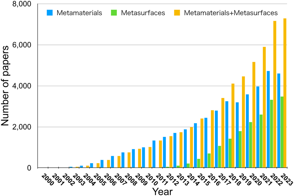
Trend in the number of publications on metamaterials research.
This special issue, “Metamaterials and Plasmonics in Asia,” was developed from the A3 Metamaterials Forum held from June 26th to 29th, 2023, at Kyoto Institute of Technology in Kyoto, Japan. The A3 Metamaterials Forum is an annual meeting that discusses cutting-edge research results in metamaterials and plasmonics among three Asian countries: Korea, Japan, and China.
Five review articles are presented in this special issue. Zhang et al. provide an overview of recent progresses in programmable optical meta-holograms and provide outlook on the challenges and prospects in this growing area [2]. Deng et al. summarize inverse design techniques for photonic crystal structures [3]. Fu et al. discuss the contribution of the machine learning techniques to advanced metasurface research [4]. Chu et al. review recent advances in thermal emission control by metasurface technologies and propose their infrared applications, such as infrared sensing, radiative cooling, and thermophotovoltaic devices [5]. Ding et al. review spectral imaging techniques using metasurface devices [6].
In addition to these review articles, this issue also contains 20 original papers. Kang et al. propose an ultrafast imaging technique of terahertz electric potentials across ring-shaped quantum barriers [7]. Shi et al. propose a zoom metalens fabricated on a flexible thin PDMS film. By stretching the substrate, focal length of the metalens could be changed and a 2× range of free magnification control was demonstrated [8]. Zhu et al. develop a spatiotemporal metasurface for beamforming applications, eliminating the Doppler effect of fast-moving automobiles, trains, aircrafts, and so on, using tandem neural network system [9]. Nakayama et al. report on a metasurface absorber for enhancing the conversion efficiency in the thermoelectric device of BiSbTe [10]. Sang et al. propose the concept of relative shift-induced quasi-bound states in the continuum and demonstrate asymmetry parameter-insensitive resonant modes using an array of silicon square disk dimers [11]. Xue et al. demonstrate a beam shaper metasurface doublet that converts a Gaussian beam into a flat-top beam using the complex-amplitude constraint Gerchberg–Saxton algorithm [12]. Guo et al. discuss the robustness of an integrated topological interface of valley photonic crystals against sharp bending [13]. Yan et al. report on-chip transmissible topological edge states using one-dimensional Su–Shrieffer–Heeger photonic crystals with defect cavities on a silicon-on-insulator slab and demonstrate wavelength division multiplexer devices [14]. Hong et al. also report a color router metasurface that can split the spectrum from visible to near-infrared and redirect it to the four optical channels (red, green, blue, and near-infrared) of a CMOS image sensor [15]. Lee et al. propose a deterministic reflection contrast ellipsometry technique for multilayer 2D heterostructures [16]. Yamaguchi et al. demonstrate a high-resolution (2322 × 2322 pixels) and full-color holographic movie using silicon nitride metasurface [17]. Ikeda et al. discuss the spatial and temporal properties of emission enhancement in InGaN/GaN by surface plasmon resonance [18]. Liu et al. introduce the diffractive neural network technique into a dielectric metasurface made of silicon and applied it to a 1 bit adder as an optical computing component [19]. Kim and Park demonstrate a perfect waveguide coupler with universal impedance matching [20]. Kim et al. propose the realization of two-dimensional Bravais lattice patterns formed by a metasurface-based interference lithography technique [21]. Lee et al. discuss the contribution of the hBN layers to the enhancement of the guided exciton–polariton modes in multilayer waveguides of WS2 [22]. Park et al. propose a sample-efficient inverse design algorithm of freeform nanophotonic devices using a physics-informed reinforcement learning technique [23]. Dai et al. report spintronic terahertz emission from a metasurface using scanning near-field nanoscopy [24]. Liu et al. propose thin film electro-optic modulator using lithium niobate [25]. Zhang et al. demonstrate holographic communication using programmable metasurafces [26].
We, symposium organizers, believe that this special issue provides a comprehensive overview of recent research activities by leading scientists in the field of metamaterials and plasmonics in Asia. Finally, we sincerely appreciate all contributions from the authors to this special issue.
-
Research funding: None declared.
-
Author contributions: All authors have accepted responsibility for the entire content of this manuscript and approved its submission.
-
Conflict of interest: Authors state no conflicts of interest.
-
Data availability: Data sharing is not applicable to this article as no datasets were generated or analyzed during the current study.
References
[1] N. Yu, et al.., “Light propagation with phase discontinuities: generalized laws of reflection and refraction,” Science, vol. 334, pp. 333–337, 2011. https://doi.org/10.1126/science.1210713.Search in Google Scholar PubMed
[2] J. C. Zhang, et al.., “Programmable optical meta-holograms,” Nanophotonics, vol. 13, no. 8, pp. 1201–1217, 2024.10.1515/nanoph-2023-0544Search in Google Scholar
[3] R. Deng, W. Liu, and L. Shi, “Inverse design in photonic crystals,” Nanophotonics, vol. 13, no. 8, pp. 1219–1237, 2024.10.1515/nanoph-2023-0750Search in Google Scholar
[4] Y. Fu, et al.., “Unleashing the potential: AI empowered advanced metasurface research,” Nanophotonics, vol. 13, no. 8, pp. 1239–1278, 2024.10.1515/nanoph-2023-0759Search in Google Scholar
[5] Q. Chu, F. Zhong, X. Shang, Y. Zhang, S. Zhu, and H. Liu, “Controlling thermal emission with metasurfaces and its applications,” Nanophotonics, vol. 13, no. 8, pp. 1279–1301, 2024.10.1515/nanoph-2023-0754Search in Google Scholar
[6] K. Ding, et al.., “Snapshot spectral imaging: from spatial spectral mapping to metasurface-based imaging,” Nanophotonics, vol. 13, no. 8, pp. 1303–1330, 2024.10.1515/nanoph-2023-0867Search in Google Scholar
[7] T. Kang, R. H. J. Kim, J. Lee, M. Seo, and D.-S. Kim, “Ultrafast snapshots of terahertz electric potentials across ring-shaped quantum barriers,” Nanophotonics, vol. 13, no. 8, pp. 1331–1338, 2024.10.1515/nanoph-2023-0538Search in Google Scholar
[8] Y. Shi, et al.., “Ultra-thin, zoom capable, flexible metalenses with high focusing efficiency and large numerical aperture,” Nanophotonics, vol. 13, no. 8, pp. 1339–1349, 2024.10.1515/nanoph-2023-0561Search in Google Scholar
[9] X. Zhu, et al.., “On-demand Doppler-offset beamforming with intelligent spatiotemporal metasurfaces,” Nanophotonics, vol. 13, no. 8, pp. 1351–1360, 2024.10.1515/nanoph-2023-0569Search in Google Scholar
[10] R. Nakayama, S. Saito, T. Tanaka, and W. Kubo, “Metasurface absorber enhanced thermoelectric conversion,” Nanophotonics, vol. 13, no. 8, pp. 1361–1368, 2024.10.1515/nanoph-2023-0653Search in Google Scholar
[11] T. Sang, et al.., “Achieving asymmetry parameter-insensitive resonant modes through relative shift–induced quasi-bound states in the continuum,” Nanophotonics, vol. 13, no. 8, pp. 1369–1377, 2024.10.1515/nanoph-2023-0673Search in Google Scholar
[12] D. Xue, et al.., “Collimated flat-top beam shaper metasurface doublet based on the complex-amplitude constraint Gerchberg–Saxton algorithm,” Nanophotonics, vol. 13, no. 8, pp. 1379–1385, 2024.10.1515/nanoph-2023-0719Search in Google Scholar
[13] C.-H. Guo, G.-J. Tang, M.-Y. Li, W.-J. Chen, X.-T. He, and J.-W. Dong, “Quantifying robustness against sharp bending in an integrated topological interface of valley photonic crystals,” Nanophotonics, vol. 13, no. 8, pp. 1387–1395, 2024.10.1515/nanoph-2023-0727Search in Google Scholar
[14] Q. Yan, R. Ma, Q. Lyu, X. Hu, and Q. Gong, “Transmissible topological edge states based on Su–Schrieffer–Heeger photonic crystals with defect cavities,” Nanophotonics, vol. 13, no. 8, pp. 1397–1406, 2024.10.1515/nanoph-2023-0744Search in Google Scholar
[15] Y. J. Hong, B. J. Jeon, Y. G. Ki, and S. J. Kim, “A metasurface color router facilitating RGB-NIR sensing for an image sensor application,” Nanophotonics, vol. 13, no. 8, pp. 1407–1415, 2024.10.1515/nanoph-2023-0746Search in Google Scholar
[16] K. R. Lee, J. G. Youn, and S. J. Yoo, “Deterministic reflection contrast ellipsometry for thick multilayer two-dimensional heterostructures,” Nanophotonics, vol. 13, no. 8, pp. 1417–1424, 2024.10.1515/nanoph-2023-0753Search in Google Scholar
[17] M. Yamaguchi, H. Saito, S. Ikezawa, and K. Iwami, “Highly-efficient full-color holographic movie based on silicon nitride metasurface,” Nanophotonics, vol. 13, no. 8, pp. 1425–1433, 2024.10.1515/nanoph-2023-0756Search in Google Scholar
[18] K. Ikeda, et al.., “Spatial and time-resolved properties of emission enhancement in polar/semi-polar InGaN/GaN by surface plasmon resonance,” Nanophotonics, vol. 13, no. 8, pp. 1435–1447, 2024.10.1515/nanoph-2023-0758Search in Google Scholar
[19] Y. Liu, W. Chen, X. Wang, and Y. Zhang, “All dielectric metasurface based diffractive neural networks for 1-bit adder,” Nanophotonics, vol. 13, no. 8, pp. 1449–1458, 2024.10.1515/nanoph-2023-0760Search in Google Scholar
[20] M. Kim and Q.-H. Park, “The perfect waveguide coupler with universal impedance matching and transformation optics,” Nanophotonics, vol. 13, no. 8, pp. 1459–1466, 2024.10.1515/nanoph-2023-0771Search in Google Scholar
[21] M. Kim, N. Kim, and J. Shin, “Realization of all two-dimensional Bravais lattices with metasurface-based interference lithography,” Nanophotonics, vol. 13, no. 8, pp. 1467–1474, 2024.10.1515/nanoph-2023-0786Search in Google Scholar
[22] H. S. Lee, J. Sung, D.-J. Shin, and S.-H. Gong, “The impact of hBN layers on guided exciton–polariton modes in WS2 multilayers,” Nanophotonics, vol. 13, no. 8, pp. 1475–1482, 2024.10.1515/nanoph-2023-0822Search in Google Scholar
[23] C. Park, et al.., “Sample-efficient inverse design of freeform nanophotonic devices with physics-informed reinforcement learning,” Nanophotonics, vol. 13, no. 8, pp. 1483–1492, 2024.10.1515/nanoph-2023-0852Search in Google Scholar
[24] M. Dai, et al.., “Spintronic terahertz metasurface emission characterized by scanning near-field nanoscopy,” Nanophotonics, vol. 13, no. 8, pp. 1493–1502, 2024.10.1515/nanoph-2023-0858Search in Google Scholar
[25] J. Liu, et al., “Lithium niobate thin film electro-optic modulator,” Nanophotonics, vol. 13, no. 8, pp. 1503–1508, 2024.10.1515/nanoph-2023-0865Search in Google Scholar
[26] F. Zhang, et al.., “Holographic communication using programmable coding metasurface,” Nanophotonics, vol. 13, no. 8, pp. 1509–1519, 2024.10.1515/nanoph-2023-0925Search in Google Scholar
© 2024 the author(s), published by De Gruyter, Berlin/Boston
This work is licensed under the Creative Commons Attribution 4.0 International License.
Articles in the same Issue
- Frontmatter
- Editorial
- Editorial on special issue “Metamaterials and Plasmonics in Asia”
- Reviews
- Programmable optical meta-holograms
- Inverse design in photonic crystals
- Unleashing the potential: AI empowered advanced metasurface research
- Controlling thermal emission with metasurfaces and its applications
- Snapshot spectral imaging: from spatial-spectral mapping to metasurface-based imaging
- Research Articles
- Ultrafast snapshots of terahertz electric potentials across ring-shaped quantum barriers
- Ultra-thin, zoom capable, flexible metalenses with high focusing efficiency and large numerical aperture
- On-demand Doppler-offset beamforming with intelligent spatiotemporal metasurfaces
- Metasurface absorber enhanced thermoelectric conversion
- Achieving asymmetry parameter-insensitive resonant modes through relative shift–induced quasi-bound states in the continuum
- Collimated flat-top beam shaper metasurface doublet based on the complex-amplitude constraint Gerchberg–Saxton algorithm
- Quantifying robustness against sharp bending in an integrated topological interface of valley photonic crystals
- Transmissible topological edge states based on Su–Schrieffer–Heeger photonic crystals with defect cavities
- A metasurface color router facilitating RGB-NIR sensing for an image sensor application
- Deterministic reflection contrast ellipsometry for thick multilayer two-dimensional heterostructures
- Highly-efficient full-color holographic movie based on silicon nitride metasurface
- Spatial and time-resolved properties of emission enhancement in polar/semi-polar InGaN/GaN by surface plasmon resonance
- All dielectric metasurface based diffractive neural networks for 1-bit adder
- The perfect waveguide coupler with universal impedance matching and transformation optics
- Realization of all two-dimensional Bravais lattices with metasurface-based interference lithography
- The impact of hBN layers on guided exciton–polariton modes in WS2 multilayers
- Sample-efficient inverse design of freeform nanophotonic devices with physics-informed reinforcement learning
- Spintronic terahertz metasurface emission characterized by scanning near-field nanoscopy
- Lithium niobate thin film electro-optic modulator
- Holographic communication using programmable coding metasurface