Nonthermal laser ablation of high-efficiency semitransparent and aesthetic perovskite solar cells
-
Junjie Zhao
 ,
Nianyao Chai
,
Xiangyu Chen
,
Nianyao Chai
,
Xiangyu Chen


Abstract
Perovskite solar cells (PSC) offer a promising solution for building integrated photovoltaics (BIPVs) due to its high photoelectric conversion efficiency (PCE). However, increasing the transparency of their functional layers dramatically decreases the PCE. Here, a computer controlled laser patterning method was proposed to directly turn PSC modules into semitransparent and with aesthetic artificial pattern, without additional complexities to the conventional PSCs fabrication process. A structured ST-PSC achieving a champion PCE of 17.5% with average visible transparency (AVT) of 18.2%, and a mini-module with 5 × 5 cm2 delivering a PCE of 9.1% with AVT of 37.7% were demonstrated. Rationally designed aesthetic patterns were imprinted on mini-modules, achieving a PCE of 14.4%. These results reveal a new route for low-cost facile fabricating high performance large-area aesthetic BIPV modules, and represent a big step forward toward the fabrication of solar cells with high efficiency and high transparency.
1 Introduction
Turning cities into power plants is a promising strategy to alleviate the imminent energy crisis [1], [2], [3]. The key point is to find a low-cost and effective way to convert solar energy into electricity in the city area [4]. Integrating transparent photovoltaic devices into buildings is one of the most effective solutions [5]. Due to the attractive opto-electronic properties of perovskite, semi-transparent perovskite solar cells (ST-PSCs) are considered as an excellent candidate providing both shading and green electricity to the building [6]. However, it is contradictory to simultaneously improve the visibility (transparency), PCE and aesthetics of ST-PSCs.
So far, to achieve high AVT of ST-PSCs, the main focus was on the manufacture of transparent perovskite absorber layers and electrodes. A simple strategy is to reduce the thickness of the perovskite film to obtain better visibility [7, 8]. However, as the absorber layer becomes thinner, to achieve a uniform, high surface coverage and pinhole-free thin film becomes a big challenge [9], [10], [11]. Therefore, creating light passing channels with microstructures on the absorber layer is straightforward to increase the transparency of PSCs [12], [13], [14], [15]. An ST-PSC with nanopillar perovskite films yielding a maximum PCE of 10.8% with an AVT of 37.4% was achieved [16]. Except making perovskite layer transparent, ST-PSCs cannot be achieved without transparent electrodes. To achieve high performance transparent electrodes, various techniques have been reported, such as sputtering transparent conductive oxides and thin metals [17, 18], conductive polymers [19], and carbon materials [20], [21], [22]. However, unavoidable damage to underneath functional layers based on current techniques leads to poor performance of ST-PSCs [23]. Therefore, finding a strategy to fabricate both high quality transparent perovskite layer and electrodes is critical for achieving high efficient ST-PSCs.
Herein, a non-thermal ablation technique was proposed to directly fabricate ST-PSCs via femtosecond laser direct writing. The ultrafast energy deposition on each functional layer with femtosecond pulses, enabling removal of all materials by suppressing thermal diffusion into a constraint zone. As a result, low loss micromesh structures were designed and imprinted on the whole cell, directly turning all the functional layers into transparency. Under optimal conditions, a record high 17.5% PCE with 18.2% AVT single junction device, and a mini-module with 5 × 5 cm2 delivering a PCE of 9.1% with AVT of 37.7% were achieved. In addition, rationally designed aesthetic mini-modules achieving PCE of 14.4% were also demonstrated.
2 Results and discussion
As depicted in Figure 1, to improve the transparency, micromesh structures were etched through all functional layers in a single step via femtosecond laser direct writing. The light can directly pass through the microstructures. The PSCs obtained by this strategy are semitransparent and artistic, which are suitable for BIPVs. Compared with traditional methods, this approach exhibits a high-efficient and low-cost process which does not require manufacturing thin absorber layer and special transparent electrodes. Most importantly, with computer assisted design, artificially aesthetic patterns can be easily imprinted on a whole PSC module to match the aesthetical design of buildings. A peacock pattern was imprinted on a 5 × 5 cm2 mini-module, keeping a PCE of 12.9%. By fabricating micromesh structures on PSC cells, we can obtain both transparent and high efficient ST-PSCs. We compared our results with the other data reported in the literature by plotting the PCEs of traditional and emerging semi-transparent PVs as a function of the corresponding AVTs. The PCEs achieved in this work were the best than those with comparable transparency reported in the collected literature.
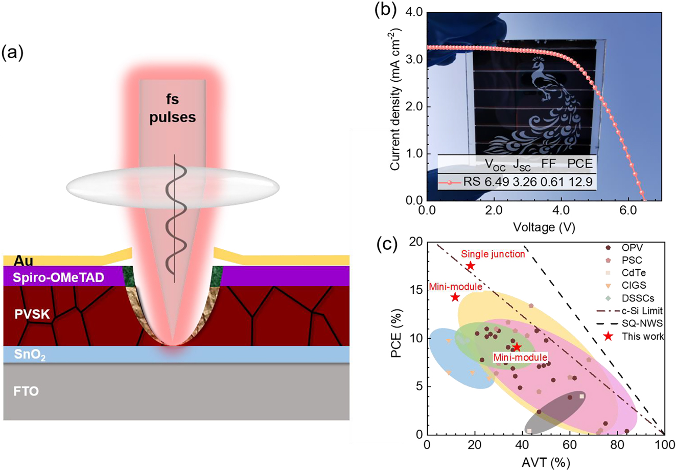
Semi-transparent perovskite solar cells (ST-PSCs) prepared by femtosecond laser direct writing.
(a) Schematic of the ablation of a whole PSC cell with all functional layers by a femtosecond laser pulse. (b) Photo and J-V test of a fabricated aesthetic PSC mini-module with 5 × 5 cm2 (c) plot of PCE with respect to AVT for transparent and semitransparent PVs reported in the literature. The dash-dot line indicates the theoretical Shockley–Queisser limit for non-wavelength selective PVs. See Table S5 for the detailed reference table.
During the exposure of femtosecond laser pulse, ionization, heating and vaporization do not occur, because the electron-to-ion energy transfer, electron heat conduction and the hydrodynamic takes much longer than the pulse duration, roughly at picosecond time scale [24], [25], [26], [27]. Hence, heat diffusion is frozen during the interaction of the laser pulse with material for picoseconds or shorter laser pulses, which offers greatly reduced thermal damage and heat affected zone (HAZ) on PSCs. Figure S1 shows a stronger decomposition of the perovskite film irradiated by the longer laser pulse in the focusing region at the same pulse energy. For same pulse energy, the peak intensity for longer pulse duration is proportional lower (Figure S1a). Thus, only in a smaller region, the deposited laser fluence reaches the ablation threshold, leading to a smaller ablation crater. Figure 2(a) shows the theoretical size of the ablation zone comparing different pulse durations at the same pulse energy, with laser wavelength 1030 nm and focusing numerical aperture (NA) 0.05. This effect can be observed from the confocal fluorescence images (Figure S1b). The ablation threshold of the perovskite film at different pulse duration was measured by fitting the measured diameters of the ablation crater relatively to the deposition fluence by Eq. (1) [28]:
where

The laser processing parameters of perovskite.
(a) The energy intensity distribution of the laser focal plane with different pulse widths. (b) Plot of squared diameter D2 of ablated area with respect to fluence for pulse widths d = 260 fs, 500 fs, 1 ps, 2 ps, 5 ps and 10 ps. (c) Squared diameter D2 of the ablation area (solid markers) and the through hole (hollow markers) produced in the 550 nm thick perovskite film under exposure duration τ = 15 µs, 55 µs, 90 µs (referring to the scanning speed
There are two distinct regions in the laser exposure area on the perovskite film as shown in Figure 2(c) inset. One is the HAZ (D1 − D2), and the other is the ablated through hole (D2). The perovskite film is decomposed due to the local temperature arising in the HAZ, as shown in Figure S1b. These two regions are generated by Gaussian-shaped pulses which the energy decays rapidly at the edge (Figure S2). By reducing the deposited laser fluence and exposure time, the size of the HAZ is able to be optimized. The sizes of D1 and D2 varying with the laser fluence under different laser exposure duration are shown in Figure 2(c). The decomposition threshold is about 60% lower than the ablation threshold of perovskite. The differences between the HAZ and the ablation hole (D1 − D2)/D1 respecting to the laser exposure duration under different laser fluence are illustrated in Figure 2(d). As the exposure duration increases, the relative size difference increases rapidly and then become steady. In order to improve the fabrication efficiency, a shorter exposure time with less decomposed area is preferred.
The optical micrograph and the corresponding confocal microscope images of an ablation crater array with varying the exposure duration and laser fluence are shown in Figure 3(a)–(c). For organic-inorganic hybrid perovskites, the inorganic components are tightly combined by strong covalent bonds or ionic bonds between atoms, and their lattice deformation will consume a lot of energy. Organic components are bonded together by small molecules through hydrogen bonds or van der Waals, and consume relatively little energy to cause significant lattice deformation [29]. It can be inferred that organic components are more likely to volatilize or decompose under laser irradiation than inorganic components. The photoluminescence spectrum (Figure 3(d)) confirms that the red area is the perovskite film, and the green area is PbI2 generated by decomposition of perovskite. More importantly, combining Figure 3(b) and the corresponding thickness change curve obtained from the stylus profiler (Figure 3(e)), it can be verified that as the laser fluence decreases, the thickness of perovskite layer is gradually reduced and no decomposed PbI2 is formed in the meantime, which suggests that this process highly suppresses the heat diffusion. The decomposition process leads to a heterojunction formation at the interface of the PbI2 (Eg = 2.3 eV) and the Cs0.05[FA0.85MA0.15]0.95Pb(I0.85Br0.15)3 (Eg = 1.63 eV) (Figure 3(f) and Figure S3) [30]. Both photogenerated electrons and holes diffuse to Cs0.05[FA0.85MA0.15]0.95Pb(I0.85Br0.15)3 and recombine there, resulting to an increased fluorescence intensity in the edge of the HAZ (Figure 3(c)). Time-resolved photoluminescence (TRPL) mapping of perovskite and spectra corresponding to different regions (Figure 3(g) and (h)) also illustrate the simultaneous presence of PbI2 and perovskite in the HAZ. Such PbI2 inclusions can act as a passivation layer for nonradiative defects on the perovskite film [31].

PL and lifetime properties of perovskite films with circular-shaped microholes array.
(a) Optical micrograph of perovskite film with circular-shaped micro craters. (b) and (c) Confocal fluorescent images of the typical areas. (d) Photoluminescence (PL) spectra of perovskite films and HAZ, respectively. (e) Stylus profiler image of perovskite film with circular-shaped micro craters. (f) Schematic of the type-I heterostructure for the study of the carrier boundary transportation. Both electrons and holes transfer from PbI2 to perovskite. (g) Time-resolved PL (TRPL) mapping of perovskite films. (h) TRPL spectra of selected areas.
For directly ablating whole PSCs, the ablation threshold of the light blocking layers such as the Spiro-MeOTAD layer and Au layer above the perovskite were also investigated. As shown in Figure S4a and b, the ablation thresholds of Spiro-MeOTAD and Au are slightly larger than perovskite, which is beneficial for removing these three materials in one step. The Spiro-MeOTAD and Au located above the perovskite will absorb part of the energy of the laser, so the laser fluence can be appropriately increased to ensure the complete removal of the materials. Besides, the threshold of FTO/ETL (Figure S4c) is much greater than that of other layers, so it can be guaranteed that FTO/ETL will not be damaged during laser processing with a safe fabrication window. The PSCs were prepared through a traditional facile solution based process combined with vacuum evaporation metal electrode. The PSC device fabrication process is depicted in Figure S5a. As shown in Figure S5b, a certain area of the fabricated PSCs is removed by a femtosecond laser, and then an ST-PSCs with a micromesh structure is formed. SEM image and the corresponding confocal fluorescent image (Figure S6) demonstrate that the perovskite layer is almost completely removed, exposing the clean FTO/ETL layer. The removed area has a direct effect on the AVT of ST-PSCs. Figure 4 shows the transmission curve of ST-PSCs caused by increasing the side length of removed square. Obviously, the more removed areas, the greater AVT of the device can be achieved. Figure 4(b) indicates the direct proportional relationship between the removal area rate and AVT. For the simplicity of the test, we adopted a mask-assisted PCE test with an effective area of 17.1 cm2 for 6 × 6 cm2 mini-module and an effective area of 10 cm2 for 5 × 5 cm2 mini-module (Figure 4(c)). Finally, we achieved a single-junction ST-PSCs with PCE of 17.5% and AVT of 18.2% (Figure S7a). Furthermore, we achieved large-area 5 × 5 cm2 mini-module with PCE of 9.1% and AVT of 37.7% and 6 × 6 cm2 mini-module with PCE of 14.1% and AVT of 11.8% (Figure 4(d) and Figure S7b). As shown in Figure 4(d), ST-PSCs fabricated by the femtosecond laser exhibit excellent semitransparent property (See Figure S8 for the detailed AVT curve.).

Photovoltaic performance characterizations of ST-PSCs.
(a) The transmission curve of ST-PSCs is caused by increasing the side length of the removed square. (b) Transmission and PCE loss are linearly fitted as a function of the removal area. (c) Schematic diagram of mask-assisted PCE test. (d) Comparison of the current−voltage characteristics of 5 × 5 cm2 PSCs before and after laser ablation.
To further evaluate the role of the proposed ST-PSCs manufacturing method, various rationally designed patterns are imprinted directly on the PSCs. The PSCs imprinted with origami and symmetrical flowers patterns (Figure 5(a) and (b)) can maintain efficiencies of 13.7% and 14.4%, respectively. For more complicated patterns, the PSCs patterned with asymmetric peacock and Chinese characters “Fu” (Figure S9) maintain efficiencies of 12.9% and 12.7%, respectively. This approach offers a totally new route for design and fabricate PSCs. Rational design and broaden applications can be utilized with PSCs for power generation. Figure 5(c) and (d) shows a beautiful designed perovskite solar cell Christmas card fabricated by this technique, which delivers excellent light conversion efficiency even at low light intensity.

Photovoltaic performance characterizations of rationally designed patterned PSCs. Current−voltage characteristics of PSCs imprinted with (a) origami and (b) symmetrical flowers patterns. (c) and (d) Photo of a PSC Christmas card and lightening more than 35 LEDs under the irradiation of a low intensity dark blue LED lamp.
3 Conclusions
In summary, a computer controlled laser patterning method was proposed to directly turn PSC modules into semitransparent and with aesthetic artificial pattern. This approach is a post-patterning method without additional complexities to the conventional PSCs fabrication process, and enable to tailor the pattern upon the demands from the aesthetic building design. Under the femtosecond laser pulses, the heat effect is highly restrained and localized which enables the removal of metal electrode, hole transport layer and perovskite nearly without thermal decomposition. As a result, a structured ST-PSC achieving a champion PCE of 17.5% with average visible transparency (AVT) of 18.2%, and a mini-module with 5 × 5 cm2 delivering a PCE of 9.1% with AVT of 37.7% were demonstrated. Rationally designed aesthetic patterns on mini-modules also achieved a PCE of 14.4%. This strategy makes it promising for manufacturing high performance large-area aesthetic (BIPV) modules by a low-cost and facile route, with architectural appeal of a building by integration at the architectural design stage and being able to added during the initial construction.
Funding source: the Fundamental Research Funds for the Central Universities
Award Identifier / Grant number: 2020IVA068, 2021III007JC
Funding source: the Guangdong Basic and Applied Basic Research Foundation
Award Identifier / Grant number: 2020A1515110250
Funding source: the National Key Research and Development Program of China
Award Identifier / Grant number: 2020YFA071500
Funding source: Foshan Xianhu Laboratory of the Advanced Energy Science and Technology Guangdong Laboratory
Award Identifier / Grant number: XHT2020-005
-
Author contribution: All the authors have accepted responsibility for the entire content of this submitted manuscript and approved submission.
-
Research funding: This work was supported by the National Key Research and Development Program of China (2020YFA0715000), Foshan Xianhu Laboratory of the Advanced Energy Science and Technology Guangdong Laboratory (XHT2020-005), the Fundamental Research Funds for the Central Universities (2020IVA068, 2021III007JC) and the Guangdong Basic and Applied Basic Research Foundation (2020A1515110250). The authors thank Guangyao Tan, Chao Wang, Yanping Mo, and Jing Li for assistance with data analysis and the PSCs fabrication.
-
Conflict of interest statement: The authors declare that they have no known competing financial interests or personal relationships that could have appeared to influence the work reported in this paper.
References
[1] D. Liu, C. Yang, and R. R. Lunt, “Halide perovskites for selective ultraviolet-harvesting transparent photovoltaics,” Joule, vol. 2, pp. 1827–1837, 2018, https://doi.org/10.1016/j.joule.2018.06.004.Search in Google Scholar
[2] R. F. Service, “See-through solar cells could power offices,” Science, vol. 360, p. 1386, 2018, https://doi.org/10.1126/science.360.6396.1386.Search in Google Scholar PubMed
[3] C. J. Traverse, R. Pandey, M. C. Barr, and R. R. Lunt, “Emergence of highly transparent photovoltaics for distributed applications,” Nat. Energy, vol. 2, pp. 849–860, 2017, https://doi.org/10.1038/s41560-017-0016-9.Search in Google Scholar
[4] B. Chen, Y. Bai, Z. Yu, et al.., “Efficient semitransparent perovskite solar cells for 23.0%-efficiency perovskite/silicon four-terminal tandem cells,” Adv. Energy Mater., vol. 6, p. 1601128, 2016, https://doi.org/10.1002/aenm.201601128.Search in Google Scholar
[5] X. Hu, X. Meng, L. Zhang, et al.., “A mechanically robust conducting polymer network electrode for efficient flexible perovskite solar cells,” Joule, vol. 3, pp. 2205–2218, 2019, https://doi.org/10.1016/j.joule.2019.06.011.Search in Google Scholar
[6] Q. Xue, R. Xia, C. J. Brabec, and H.-L. Yip, “Recent advances in semi-transparent polymer and perovskite solar cells for power generating window applications,” Energy Environ. Sci., vol. 11, pp. 1688–1709, 2018, https://doi.org/10.1039/c8ee00154e.Search in Google Scholar
[7] M. Batmunkh, Y. L. Zhong, and H. Zhao, “Recent advances in perovskite‐based building‐integrated photovoltaics,” Adv. Mater., vol. 32, p. 2000631, 2020, https://doi.org/10.1002/adma.202000631.Search in Google Scholar PubMed
[8] S. Rahmany and L. Etgar, “Semitransparent perovskite solar cells,” ACS Energy Lett., vol. 5, pp. 1519–1531, 2020, https://doi.org/10.1021/acsenergylett.0c00417.Search in Google Scholar
[9] B. Shi, L. Duan, Y. Zhao, J. Luo, and X. Zhang, “Semitransparent perovskite solar cells: from materials and devices to applications,” Adv. Mater., vol. 32, p. 1806474, 2020, https://doi.org/10.1002/adma.201806474.Search in Google Scholar PubMed
[10] J. Sun and J. J. Jasieniak, “Semi-transparent solar cells,” J. Phys. D Appl. Phys., vol. 50, 2017, Art no. 093001, https://doi.org/10.1088/1361-6463/aa53d7.Search in Google Scholar
[11] S. Bag and M. F. Durstock, “Efficient semi-transparent planar perovskite solar cells using a ‘molecular glue,’” Nano Energy, vol. 30, pp. 542–548, 2016, https://doi.org/10.1016/j.nanoen.2016.10.044.Search in Google Scholar
[12] G. E. Eperon, D. Bryant, J. Troughton, et al.., “Efficient, semitransparent neutral-colored solar cells based on microstructured formamidinium lead trihalide perovskite,” J. Phys. Chem. Lett., vol. 6, pp. 129–138, 2015, https://doi.org/10.1021/jz502367k.Search in Google Scholar PubMed
[13] L. Zhang, M. T. Hörantner, W. Zhang, Q. Yan, and H. J. Snaith, “Near-neutral-colored semitransparent perovskite films using a combination of colloidal self-assembly and plasma etching,” Sol. Energy Mater. Sol. Cell., vol. 160, pp. 193–202, 2017, https://doi.org/10.1016/j.solmat.2016.10.035.Search in Google Scholar
[14] M. T. Hörantner, W. Zhang, M. Saliba, K. Wojciechowski, and H. J. Snaith, “Templated microstructural growth of perovskite thin films via colloidal monolayer lithography,” Energy Environ. Sci., vol. 8, pp. 2041–2047, 2015, https://doi.org/10.1039/C5EE01169H.Search in Google Scholar
[15] S. Aharon, M. Layani, B.-E. Cohen, E. Shukrun, S. Magdassi, and L. Etgar, “Self-assembly of perovskite for fabrication of semitransparent perovskite solar cells,” Adv. Mater. Interfac., vol. 2, p. 1500118, 2015, https://doi.org/10.1002/admi.201500118.Search in Google Scholar
[16] H.-C. Kwon, A. Kim, H. Lee, D. Lee, S. Jeong, and J. Moon, “Parallelized nanopillar perovskites for semitransparent solar cells using an anodized aluminum oxide scaffold,” Adv. Energy Mater., vol. 6, p. 1601055, 2016, https://doi.org/10.1002/aenm.201601055.Search in Google Scholar
[17] Q. Xue, Y. Bai, M. Liu, et al.., “Dual interfacial modifications enable high performance semitransparent perovskite solar cells with large open circuit voltage and fill factor,” Adv. Energy Mater., vol. 7, p. 1602333, 2017, https://doi.org/10.1002/aenm.201602333.Search in Google Scholar
[18] M. Xie, H. Lu, L. Zhang, et al.., “Fully solution‐processed semi‐transparent perovskite solar cells with ink‐jet printed silver nanowires top electrode,” Sol. RRL., vol. 2, p. 1700184, 2018, https://doi.org/10.1002/solr.201700184.Search in Google Scholar
[19] L. Bu, Z. Liu, M. Zhang, et al.., “Semitransparent fully air processed perovskite solar cells,” ACS Appl. Mater. Interfaces, vol. 7, pp. 17776–17781, 2015, https://doi.org/10.1021/acsami.5b04040.Search in Google Scholar PubMed
[20] Z. Li, S. A. Kulkarni, P. P. Boix, et al.., “Laminated carbon nanotube networks for metal electrode-free efficient perovskite solar cells,” ACS Nano, vol. 8, pp. 6797–6804, 2014, https://doi.org/10.1021/nn501096h.Search in Google Scholar PubMed
[21] F. R. Li, Y. Xu, W. Chen, S. H. Xie, and J. Y. Li, “Nanotube enhanced carbon grids as top electrodes for fully printable mesoscopic semitransparent perovskite solar cells,” J. Mater. Chem. A., vol. 5, pp. 10374–10379, 2017, https://doi.org/10.1039/c7ta01383c.Search in Google Scholar
[22] P. You, Z. Liu, Q. Tai, S. Liu, and F. Yan, “Efficient semitransparent perovskite solar cells with graphene electrodes,” Adv. Mater., vol. 27, pp. 3632–3638, 2015, https://doi.org/10.1002/adma.201501145.Search in Google Scholar PubMed
[23] Q. Tai and F. Yan, “Emerging semitransparent solar cells: materials and device design,” Adv. Mater., vol. 29, p. 1700192, 2017, https://doi.org/10.1002/adma.201700192.Search in Google Scholar PubMed
[24] K. Sokolowski-Tinten, J. Bialkowski, A. Cavalleri, et al.., “Transient states of matter during short pulse laser ablation,” Phys. Rev. Lett., vol. 81, pp. 224–227, 1998, https://doi.org/10.1103/physrevlett.81.224.Search in Google Scholar
[25] X. W. Wang, A. A. Kuchmizhak, X. Li, et al.., “Laser-induced translative hydrodynamic mass snapshots: noninvasive characterization and predictive modeling via mapping at nanoscale,” Phys. Rev. Appl., vol. 8, 2017, Art no. 044016, https://doi.org/10.1103/physrevapplied.8.044016.Search in Google Scholar
[26] B. C. Stuart, M. D. Feit, A. M. Rubenchik, B. W. Shore, and M. D. Perry, “Laser-induced damage in dielectrics with nanosecond to subpicosecond pulses,” Phys. Rev. Lett., vol. 74, pp. 2248–2251, 1995, https://doi.org/10.1103/physrevlett.74.2248.Search in Google Scholar
[27] A. Rousse, C. Rischel, S. Fourmaux, et al.., “Non-thermal melting in semiconductors measured at femtosecond resolution,” Nature, vol. 410, pp. 65–68, 2001, https://doi.org/10.1038/35065045.Search in Google Scholar PubMed
[28] J. J. J. Nivas, E. Allahyari, A. Vecchione, Q. Hao, S. Amoruso, and X. Wang, “Laser ablation and structuring of CdZnTe with femtosecond laser pulses,” J. Mater. Sci. Technol., vol. 48, pp. 180–185, 2020, https://doi.org/10.1016/j.jmst.2020.01.059.Search in Google Scholar
[29] W. Li, Z. Wang, F. Deschler, S. Gao, R. H. Friend, and A. K. Cheetham, “Chemically diverse and multifunctional hybrid organic–inorganic perovskites,” Nat. Rev. Mater., vol. 2, p. 16099, 2017, https://doi.org/10.1038/natrevmats.2016.99.Search in Google Scholar
[30] Q. Chen, H. Zhou, T.-B. Song, et al.., “Controllable self-induced passivation of hybrid lead iodide perovskites toward high performance solar cells,” Nano Lett., vol. 14, pp. 4158–4163, 2014, https://doi.org/10.1021/nl501838y.Search in Google Scholar PubMed
[31] J. Barbé, M. Newman, S. Lilliu, et al.., “Localized effect of PbI2 excess in perovskite solar cells probed by high-resolution chemical–optoelectronic mapping,” J. Mater. Chem. A., vol. 6, pp. 23010–23018, 2018, https://doi.org/10.1039/C8TA09536A.Search in Google Scholar
Supplementary Material
The online version of this article offers supplementary material (https://doi.org/10.1515/nanoph-2021-0683).
© 2022 Junjie Zhao et al., published by De Gruyter, Berlin/Boston
This work is licensed under the Creative Commons Attribution 4.0 International License.
Articles in the same Issue
- Frontmatter
- Reviews
- Photonic neuromorphic technologies in optical communications
- Photo-modulated optical and electrical properties of graphene
- Optical metasurfaces for generating and manipulating optical vortex beams
- Research Articles
- Photon coupling-induced spectrum envelope modulation in the coupled resonators from Vernier effect to harmonic Vernier effect
- Generation of high-uniformity and high-resolution Bessel beam arrays through all-dielectric metasurfaces
- Controlling and probing heat generation in an optical heater system
- Nonthermal laser ablation of high-efficiency semitransparent and aesthetic perovskite solar cells
- Plasmon-enhanced photoluminescence from MoS2 monolayer with topological insulator nanoparticle
- Polarization-controlled anisotropy in hybrid plasmonic nanoparticles
- Empirical formulation of broadband complex refractive index spectra of single-chirality carbon nanotube assembly
- Direct generation of entangled photon pairs in nonlinear optical waveguides
- A high-gain cladded waveguide amplifier on erbium doped thin-film lithium niobate fabricated using photolithography assisted chemo-mechanical etching
- High-performance near-infrared photodetectors based on gate-controlled graphene–germanium Schottky junction with split active junction
- Nonlinear thermal lensing of high repetition rate ultrafast laser light in plasmonic nano-colloids
- Ultra-secure optical encryption based on tightly focused perfect optical vortex beams