Ultracompact and low-power-consumption silicon thermo-optic switch for high-speed data
-
Ruihuan Zhang


Abstract
Ultracompact and low-power-consumption optical switches are desired for high-performance telecommunication networks and data centers. Here, we demonstrate an on-chip power-efficient 2 × 2 thermo-optic switch unit by using a suspended photonic crystal nanobeam structure. A submilliwatt switching power of 0.15 mW is obtained with a tuning efficiency of 7.71 nm/mW in a compact footprint of 60 μm × 16 μm. The bandwidth of the switch is properly designed for a four-level pulse amplitude modulation signal with a 124 Gb/s raw data rate. To the best of our knowledge, the proposed switch is the most power-efficient resonator-based thermo-optic switch unit with the highest tuning efficiency and data ever reported.
1 Introduction
Silicon photonic switches have attracted much attention thanks to their high compactness and the compatibility with the complementary metal-oxide-semiconductor fabrication process [1]. Typically, the switching between the on–off states of an on-chip silicon photonic switch can be achieved through thermo-optic (TO) tuning or electro-optic (EO) tuning process [2]. Benefitting from the large TO coefficient (1.86 × 10⁻⁴/K) of the silicon waveguide at 1.55 μm wavelength, silicon TO switches show advantages in high tuning efficiencies and compact footprints, therefore have been extensively studied for cost-effective and power-efficient optical switching networks [3], [4], [5], [6], [7].
Generally, most silicon TO switches are realized by applying overcladding heaters on top of the silicon waveguides, which can effectively prevent the metal absorption of the optical power [8], [9], [10]. However, these schemes are inherently power inefficient due to the large heat dissipations caused by the inevitable thermal spreading within the cladding oxides. In order to reduce the power consumption, it is feasible to decrease the heat dissipation, or to improve the efficiency in the tuning process of the switch. Various approaches and technologies have been proposed to reduce the power consumptions of the devices. In [11], a silicon Mach–Zehnder interferometer (MZI)–based switch was demonstrated using a highly n-type doped silicon heater that was directly contacted with the waveguide, thus decreasing the power dissipation in the heat conduction process. However, the fabrication process requires ion implantation and annealing. Some silicon TO switches added thermal isolation trenches by etching away the silicon substrates to suppress the heat diffusions, which helped to improve the tuning efficiencies [12], [13], [14], [15], [16]. However, the waveguides were still surrounded by the silica claddings, leading to limited performance improvements in the heat conduction processes. Other approaches are desired to further lower the power consumption of the silicon TO switch.
In a previous work [17], we demonstrated a power efficient switch by introducing high quality factor (Q-factor) resonators in the MZI switch. However, the accompanied narrow bandwidth with the high Q-factor limits the performance of the switch in high-speed data transmission. In this paper, we propose a scheme that can effectively lower the power consumptions of the on-chip TO switches. A suspended photonic crystal nanobeam (PCN)–based silicon TO MZI switch is fabricated as an example to illustrate the method. The PCN is designed with an ultrasmall mode volume (∼0.243 μm3) and a reasonable Q-factor (∼2000) to enable a high tuning efficiency and a sufficient bandwidth for the switch. Compared with the conventional MZI switches, the simulated tuning efficiency of the switch is dramatically improved by ∼12 times. In the experiment, a submilliwatt switching power of 0.15 mW is obtained with a device footprint of 60 μm × 16 μm. The tuning efficiency of the switch is 7.71 nm/mW with a continuous tuning range wider than 25 nm. Moreover, a high-speed data switching experiment is carried out to study the switching performance. The results exhibit a low power penalty of less than 0.5 dB at a 124 Gb/s raw data rate with a four-level pulse amplitude modulation (PAM-4) format. A fast TO switching time of ∼2 μs is also demonstrated. To the best of our knowledge, the proposed switch is the most power-efficient resonator-based TO switch unit with the highest tuning efficiency and capacity.
2 Optimization of the low power-consumption TO switch
The switching process of a conventional silicon TO MZI switch is realized by applying thermal energy to one of the waveguide arms to tune the optical phase [18]. During this process, the required phase shift of the switch can be decreased by introducing a resonant cavity into the waveguide, thus improving the tuning efficiency [19], [20], [21], [22].
In a TO tuning microresonator, the resonance frequency shift caused by the applied thermal power can be expressed as [23], [24]:
where ω 0 is the frequency of the Bloch mode, Δε is the variation of the cavity relative permittivity (ε) caused by the TO effect, E(r) is the optical field distribution of the Bloch mode. The tuning power of the resonant cavity can be further obtained by considering the heat conduction process, which can be expressed as:
where k is the TO coefficient of the silicon waveguide, C ws is the heat capacity of the heated waveguide, n is the refractive index of the silicon waveguide, Q f is the Q-factor of the resonant cavity, m is the overlap fraction between the optical field and the thermal region of the resonant cavity. The detailed mathematical description can be found in Supplementary material. According to Eq. (2), an optical switch with a low power consumption is supposed to employ a resonator with a small mode volume, a large Q f and a small C ws .
Figure 1 shows the flow chart of the optimizing process of a low-power-consumption TO tuning resonator. Firstly, an ultrasmall mode volume is helpful to reduce the tuning power of a resonator by confining the optical field in a compact region. The tightly confined optical field in the cavity can effectively overlap with a given thermal region, thus increasing the value of overlap fraction (m) [24]. In addition, the small mode volume is also helpful to achieve a uniform thermal perturbation, which leads to an efficient tuning process. Secondly, as shown in Eq. (2), the resonator is supposed to have a high enough Q-factor (Q f ) to effectively decrease the power consumption. However, a high Q-factor will result in a limited bandwidth which impairs the high-speed data (e.g., 100 Gb/s or higher). Thus, the Q-factor of the resonator should be carefully tuned to enable the low power consumption of the switch while maintaining a sufficient bandwidth [25], [ 26].
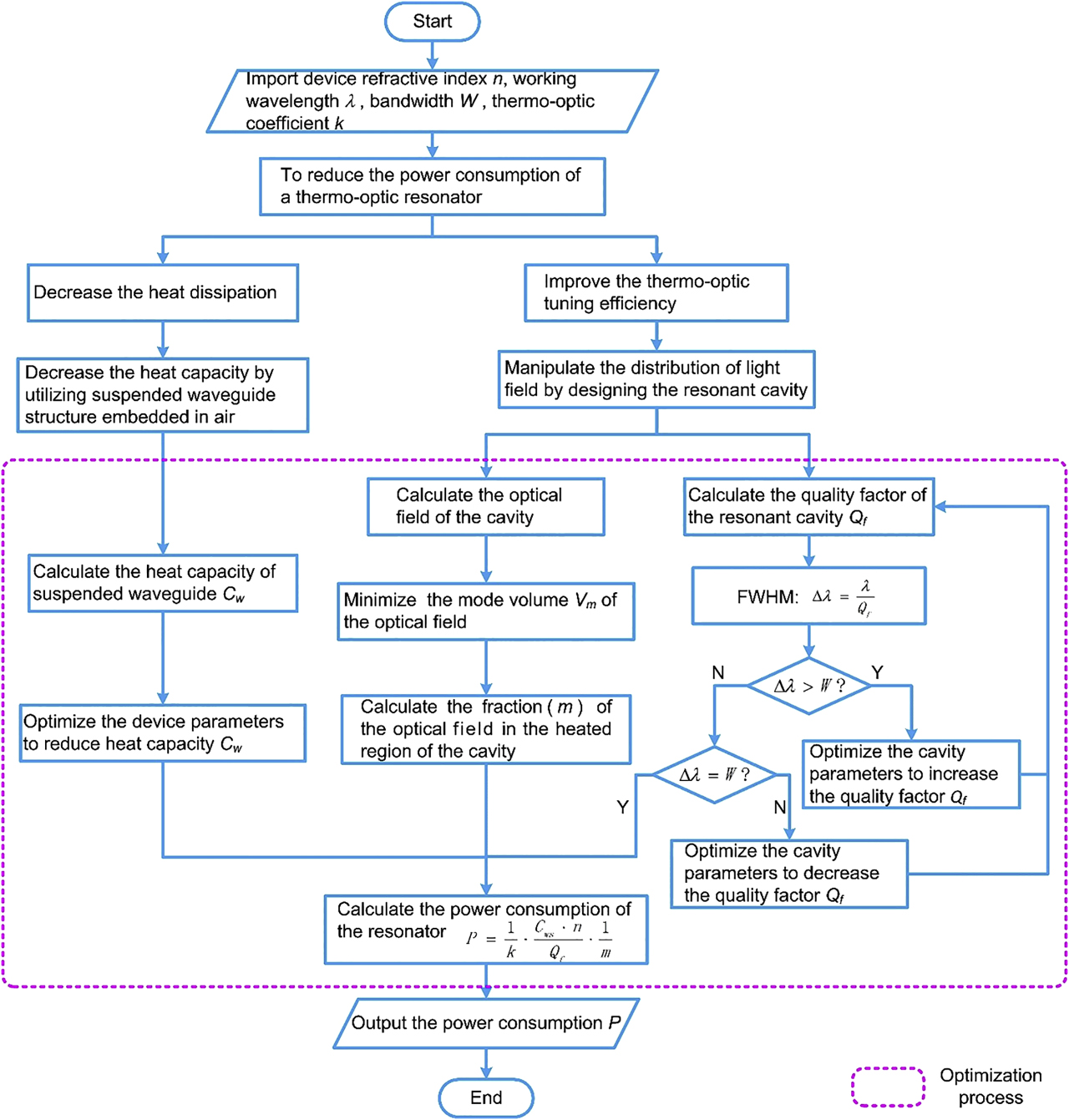
Flow chart for the optimization process of a low-power-consumption thermo-optic (TO) resonator.
Furthermore, removing the silica around the waveguide is also a viable method to reduce the power consumption by decreasing heat capacity (C ws ) [27]. Compared with a conventional silicon-on-insulator (SOI) waveguide, the suspended waveguide structure embedded in air exhibits a smaller heat capacity (C ws ) caused by the low heat conductivity coefficient of air, resulting in less thermal dissipation in the heat conduction process. Most of the heating power is confined within the metal heater and the heated waveguide, thus a high tuning efficiency can be realized for the switch, which leads to a lower power consumption.
3 Switch structure and design principle
In order to verify the optimization method, we design a 2 × 2 silicon TO MZI switch by employing two suspended PCNs. The schematic configurations of the PCN and the switch are shown in Figure 2. In order to split or combine the transmission light power equally, two directional coupler-based 50:50 power splitters are employed at the input and output ports, respectively. The waveguide widths of the splitters are designed to be 450 nm. The coupling lengths and gaps are 10 μm and 200 nm, respectively. The lengths of the two arms of MZI are designed to be equal to ensure the constructive interference happens.
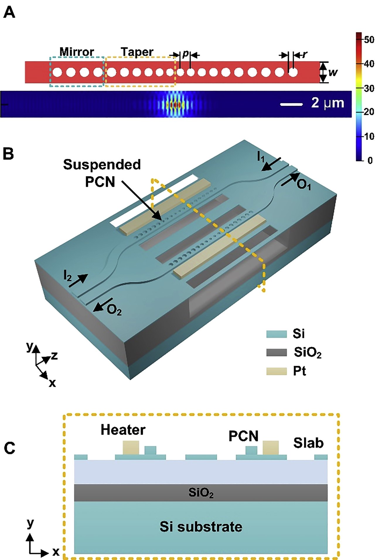
Schematic diagrams of the suspended photonic crystal nanobeam (PCN)–based Mach–Zehnder interferometer (MZI) switch.
(A) Structure and simulated optical field distribution of the PCN. (B) Device configuration of the switch. (C) Cross section of the configuration (yellow-dotted plane in B).
Two suspended PCNs with the same parameters are embedded in the two arms of MZI switch, and connected to the heaters by thin silicon slab waveguides. The schematic of the PCN cavity is illustrated in Figure 2(A). It consists of an array of 20 shallowly etched circular air holes to form a Fabry–Perot (F–P) cavity, which is symmetric with respect to its center. On each side of the cavity, the central six holes are adiabatically tapered to realize the phases matching between the waveguide mode and the Bloch mode, thus minimizing the cavity scattering loss of light. The tapered region is followed by four identical holes to serve as the reflector mirrors. The mode volume and Q-factor of the PCN cavity are iteratively optimized by using a 2.5D variational finite-difference-time-domain (FDTD) analysis tool. The optimization process can be found in our previous work [17]. In order to obtain a reasonable bandwidth for the switch, the Q-factor of the PCN is carefully tuned to be about 2000. The radii of the holes are optimized as: r (n) = d [p + 15(n − 1)], (n = 1, …, 6), r (n) = r (6), (n = 7, …, 10), d is the ratio of the radius to the period and is equal to 0.36, p is the smallest period and is equal to 344 nm. As demonstrated in Figure 2(A), the radii are r 1 = 124 nm, r 2 = 129 nm, r 3 = 134 nm, r 4 = 140 nm, r 5 = 145 nm, r 6 = 151 nm, r i = 151 nm (i = 6, 7, …, 10), respectively. The periods are p 1 = 344 nm, p 2 = 359 nm, p 3 = 374 nm, p 4 = 389 nm, p 5 = 404 nm, p i = 419 nm (i = 6, 7, 8, 9), respectively. In addition, the spacing p 0 between the two central holes is set to be 322 nm to introduce a defect for the resonant cavity. As shown in Figure 2(A), the optical field is confined within the cavity with a length of about 3 μm and a mode volume of about 0.243 μm3. The width of the PCN waveguide is w = 685 nm to reduce the in-plane radiation loss of the cavity. Four 5-μm-long tapers are used to smoothly connect the 450-nm-wide waveguides with the 685-nm-wide PCN waveguides at the front and rear ports. Figure 3 shows the simulated transmission spectra of the device. The simulated insertion loss (IL) and cross talk values are 0.5 and –30.7 dB, respectively.
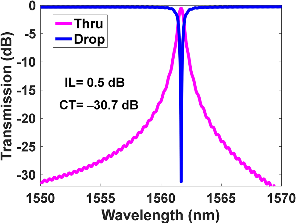
Simulated transmission spectra of the suspended photonic crystal nanobeam (PCN)–based Mach–Zehnder interferometer (MZI) switch.
Furthermore, four air trenches are employed beside the two PCNs and heaters to prevent heat spreading in the slab waveguide. The thermal cross talk of the switch is negligible due to the low heat conductivity coefficient of air in the air trenches. The center to center distance of the two PCN arms is 15.4 μm, and the widths of the air trenches are 1.86 μm. In addition, the silica under the slab waveguide is removed, which prevents the heat diffusions in the silica and silicon substrates. We have simulated the thermal distributions of the PCN waveguides using 3D finite element method simulation as shown in Figure 4. Compared with the conventional waveguide structure, the thermal field of the suspended structure is mostly confined within the PCN, benefiting from the air trench and the undercutting structure. The temperature of the suspended PCN increases from 293 to 668 K with a 1 mW heating power, which is about 12 times higher than the conventional PCN waveguide (from 293 to 324 K).

Simulated thermal fields of the photonic crystal nanobeam (PCN) waveguides.
(A) Thermal distribution of the suspended PCN waveguide (top: main view, bottom: cross section). (B) Thermal distribution of the conventional PCN waveguide (top: main view, bottom: cross section).
Considering the silicon TO effect and the electromagnetic perturbation theory, the greater temperature change indicates a larger increment of the refractive index, leading to a lager wavelength shift of the PCN. A simulated tuning efficiency of 15.62 nm/mW is obtained for a dual PCNs-based TO MZI switch. The detailed mathematical description of the TO tuning efficiency can be found in Supplementary material.
4 Device fabrication
The switch was fabricated on a SOI wafer, with a 220-nm-thick top silicon layer and a 3-μm-thick buried silica layer. The waveguides and PCNs were shallowly etched with a depth of 170 nm, while the air trenches were fully etched in the top silicon layer. The device was fabricated by using E-beam lithography technology (Vistec EBPG 5200+) and inductively coupled plasma etching process (SPTS DRIE-I). Two 300-nm-thick platinum heaters were sputtered beside the PCNs. Three pads were evaporated with 300-nm-thick gold and connected to the heaters as electrodes. The heaters and metal electrodes were fabricated by lift-off process with the length of 20 and 150 μm, respectively. Finally, the silica layer beneath the PCNs was etched by a dilute hydrofluoric acid solution to form the free-standing structure. The detailed fabrication processes of the suspended waveguide structure can be found in [28]. Figure 5 shows the microscope image and scanning electron microscope (SEM) image of the fabricated device structure. The footprint of the device is 60 μm × 16 μm. The red-dotted areas in the microscope photo and the SEM image are the air trenches, the white-boxed areas are the PCNs, and the green-dotted areas in the microscope photo are the 50:50 splitters.
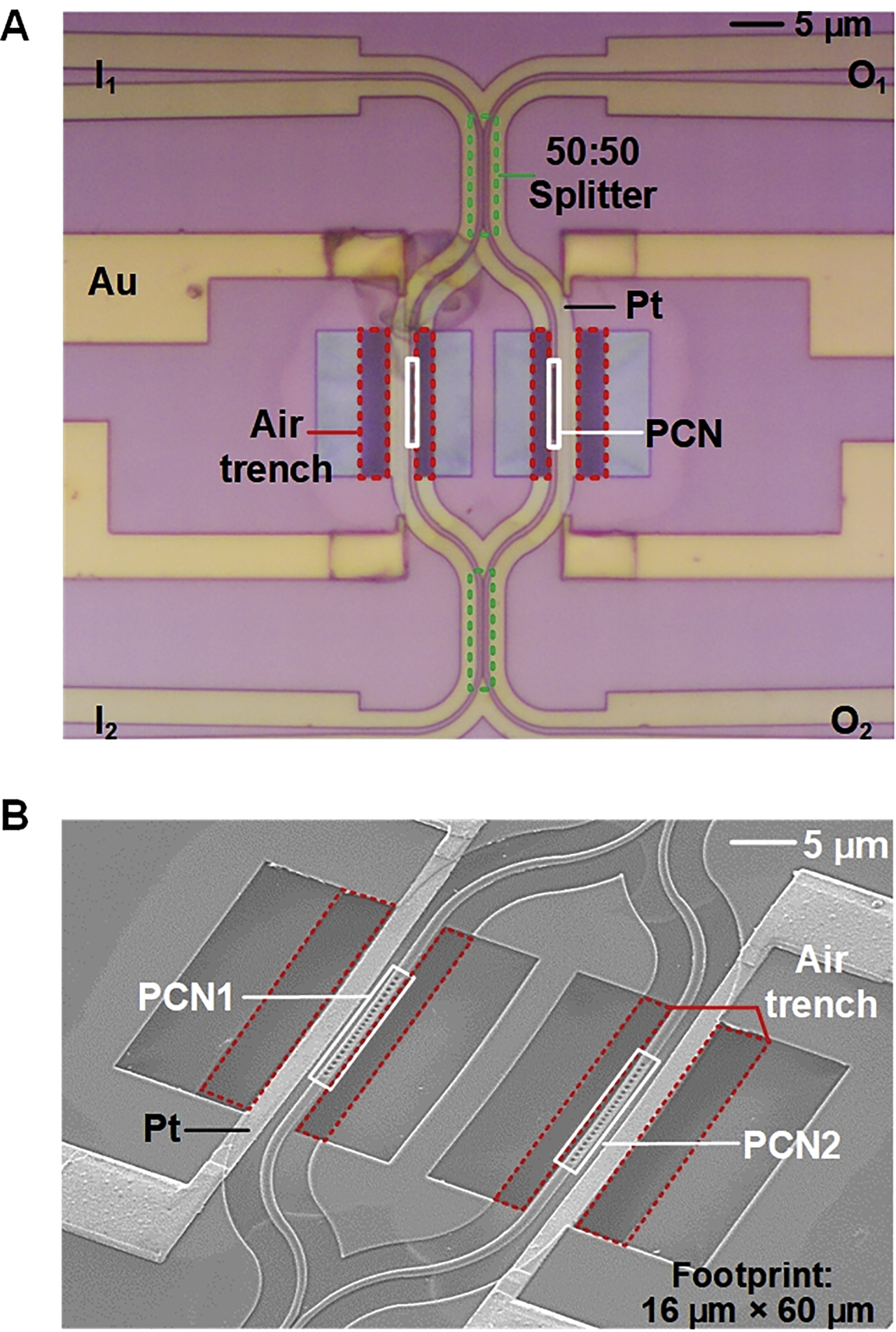
Images of the fabricated device.
(A) Microscope image of the switch. (B) Scanning electron microscope (SEM) image of the switch.
5 Experimental results and discussion
The performance of the fabricated device was characterized by using a tunable laser (Keysight 81960), an optical power meter and two voltage-current source-meters (Keithley 2400). Four photonic crystal structure-based grating couplers were adopted at the two input ports and two output ports to couple the light in and out of the device. The coupling loss of the grating coupler is 11.1 dB/facet at the central wavelength of 1550 nm according to the transmission result of a reference waveguide. The performances of the grating couplers are moderate which might be affected by the fabrication errors.
Figure 6(A) shows the unaligned transmission spectra measured at the drop port (Drop) and the through port (Thru), respectively. There is a resonance wavelength misalignment (∼9.5 nm) between the two PCNs, which is caused by the parameter deviations introduced during the fabrication process. We apply an electric power of 0.67 mW to tune the shorter resonance wavelength to make sure that the two PCNs operate in the same state. Note that this power can be minimized by improving the precision of fabrication process. When the operation wavelengths of the two PCNs are aligned at 1560.90 nm as shown in Figure 6(B), the switch works at the cross state. The crosstalk and IL are −13.5 and 4.4 dB, respectively. To switch to the bar state, the wavelength shift is expected to be more than the FWHM (full wave at half maximum) of the switch to achieve acceptable crosstalk values and realize the switching of the signal channel. The FWHM of the transmission spectrum at the through port is 0.68 nm, corresponding to a 3-dB bandwidth of 85 GHz. A tuning power of 0.15 mW is needed to tune the aligned wavelengths from 1560.90 to 1562.61 nm simultaneously. Then, most of the light outputs from the drop port at the previous resonance wavelength of 1560.90 nm as shown in Figure 6(C). At the bar state, the cross talk and IL are −13.8 and 2.0 dB, respectively. The higher experimental IL values than the simulated results are attributed to the higher cavity losses of PCNs and unequal splitting ratios of the 50:50 splitters, which were induced by the deviations of the device structural parameters introduced in the fabrication process. In practical applications, the crosstalk performance of the device can be improved by cascading several identical PCNs in each of the two arms of the MZI [29], or introducing viable power splitters at the front and rear ports of the MZI [30].
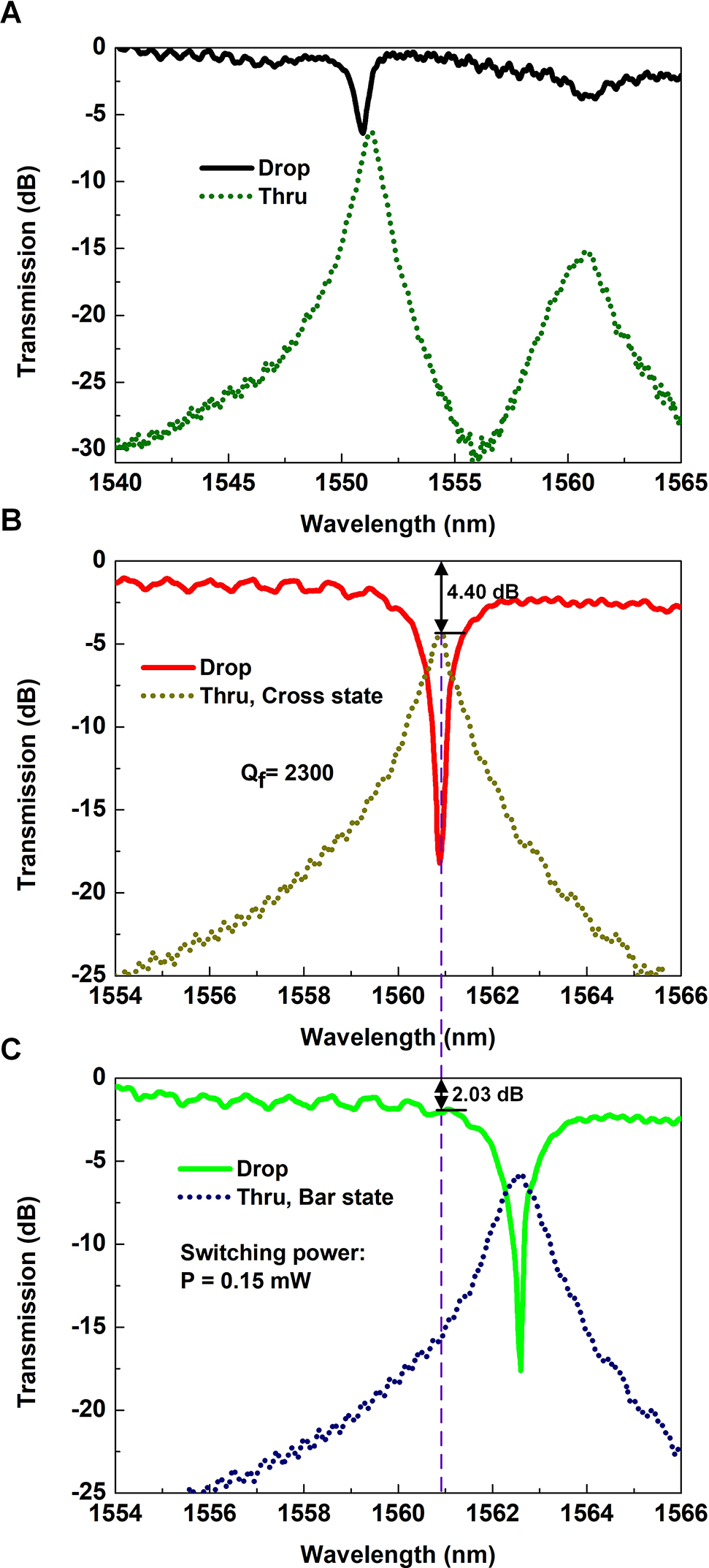
Measured transmission spectra at different states of the fabricated switch.
(A) Measured transmission spectra at the unaligned state. (B) Measured transmission spectra at the cross state. (C) Transmission spectra at the bar state of the switch. Note that the transmission spectra are normalized to a reference waveguide.
To calculate the thermal tuning efficiency of the switch, we apply different voltages to the metal heaters to collect more data. Figure 7(A) shows the transmission spectra with the applied power of P 1 = 0, P 2 = 0.15, P 3 = 0.49, P 4 = 1.15, P 5 = 1.78 mW. We choose 1560.90 nm as the operation wavelength where the switch works at the cross state. When the tuning power increases to 0.15 mW, the device is switched to the bar state. Further wavelength shifts are measured along with the tuning powers of 0.49, 1.15, and 1.78 mW. Note that the transmission spectra of the device are not flat, the ILs increase during the thermal tuning process, which may be attributed to the change of cavity losses induced by (1) the nonideal 50:50 splitters with limited operation bandwidths; and (2) nonuniform refractive index distribution induced by the heating power. These two factors cause performance deviations from the optimal designed values. In Figure 7(B), we use a curve to linearly fit the wavelength shift of the designed switch as a function of the tuning power. The slope of the fitting solid line corresponds to the tuning efficiency of the device, which is 7.71 nm/mW.
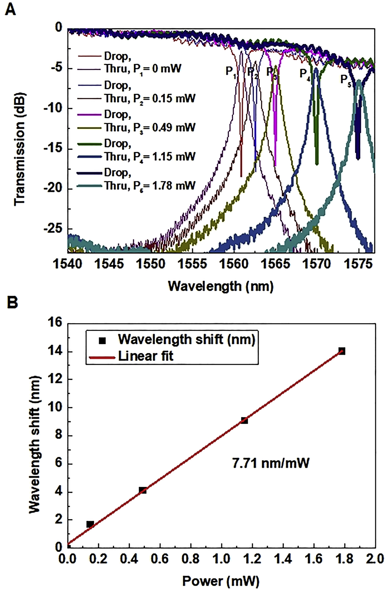
Transmission spectra of the device and the fitting curve.
(A) Transmission spectra of the fabricated switch at the drop port and the thru port with varied applying powers (P 1, P 2, P 3, P 4, P 5). (B) Fitting curve of the resonance wavelength shift against the applied power.
Furthermore, an on–off switching test is carried out to measure the response time of the switch. As shown in Figure 8, two 10-KHz square wave electric signals are loaded onto the heaters simultaneously. Then, the output signals are obtained at the drop port and through port, respectively. The signals show a rising time constant of ∼1.2 μs and a falling time constant of 2.3 μs at the drop port, a rising time constant of 2.2 μs and a falling time constant of 1.0 μs at the through port.
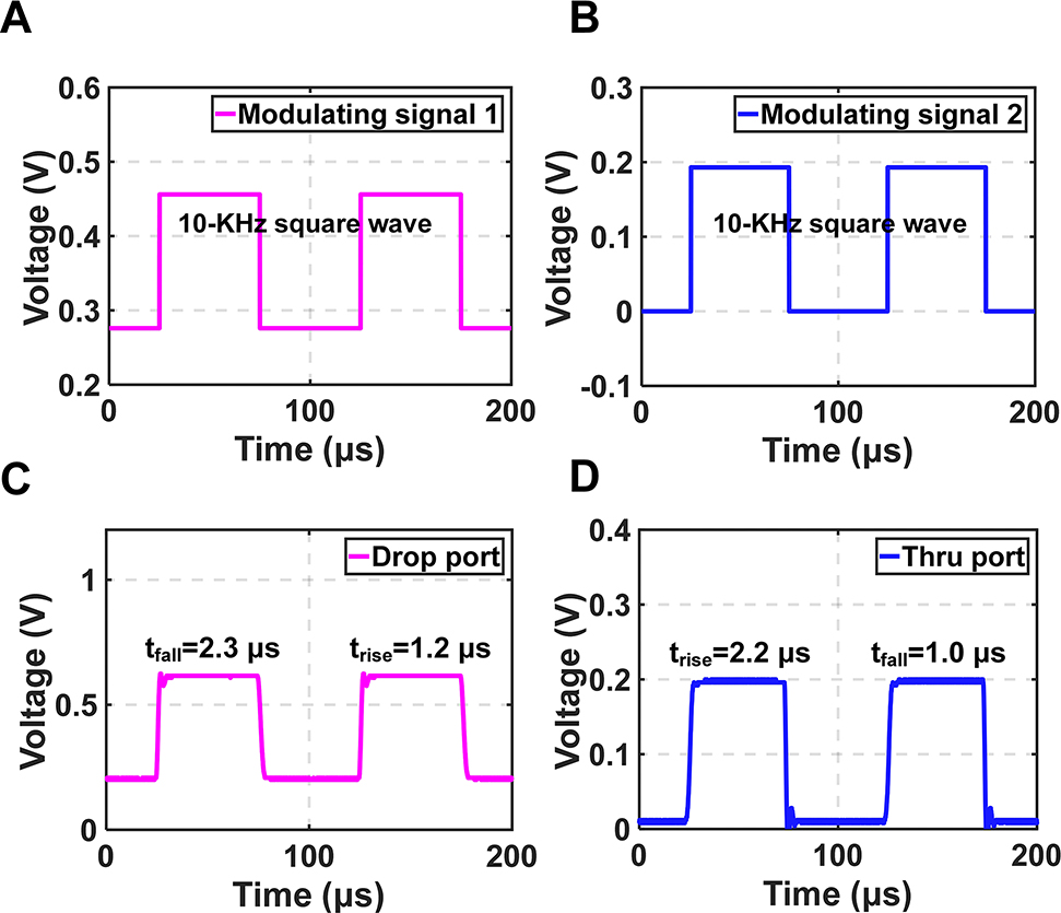
Temporal responses of the switch.
(A) The square-wave driving signal loaded onto the heater of PCN1. (B) The square-wave driving signal loaded onto the heater of PCN2. (C) The output signal from the drop port. (D) The output signal from the through port of the switch.
We provide a brief summary for previously reported on-chip 2 × 2 TO switching units in Table 1. Resonator-based switches inherently exhibit more compact device footprints relative to nonresonant structures. Overall, the proposed switch shows balanced performances, and demonstrates the lowest switching power, the highest tuning efficiency, and the compact footprint in resonator-based 2 × 2 TO switches. While most previous characterizations were limited to the device performances only, we provide in this paper the bit error ratio (BER) measurement of such a switch with a 124 Gb/s PAM-4 data, as detailed below. This is the highest reported rate in a 2 × 2 TO switch, to the best of our knowledge.
Performances of some on-chip 2 × 2 thermo-optic (TO) switching units.
| Type | Device footprint (μm2) | Switching power (mW) | Tuning efficiency (nm/mW) | IL (dB) | Cross talk (dB) | Bandwidth (nm) | Data rate (Gb/s) | Modulation format | Switching time (μs) |
|---|---|---|---|---|---|---|---|---|---|
| Adiabatic bend-based MZI [11] | ∼5000 | 12.7 | — | 0.5 | −20 | 70 | — | — | 2.2 |
| Si-PCMa [31] | ∼3 mm-length | 1.41 | — | 2 | −10 | 110 | — | — | — |
| Dual MRRs [12] | >51 × 17 | 6 | 0.91 | 4 | −20 | 0.2 | — | — | 9 |
| MRR [32] | 15 × 15 | ∼ 3 | 0.39 | ∼2 | −9.5 | 0.32 | 12.5 | OOK | — |
| Folded-waveguide MIb [15] | 400 × 130 | 0.05 | — | 3.3 | −26 | >10 | — | — | 780 |
| Photonic crystal [33] | 15 × 15 | 3 | 1.17 | <1 | <–20 | ∼3 | — | — | 2.91 |
| Cascaded PCNs-based MZI [19] | 150 × 30 | 0.16 | 1.23 | 1.5 | −15 | 0.09 | — | — | 4.5 |
| Dual PCNs-based MZI [17] | 75 × 15 | 0.24 | 0.66 | 1.5 | −15 | 0.12 | — | — | 2.5 |
| This work | 60 × 16 | 0.15 | 7.71 | 4.4 | −13.5 | 0.68 | 124 | PAM-4 | 2.3 |
-
aPCM, Phase change material; bMI, Michelson interferometer.
Here we detail the transmission performance of a 62-GBaud PAM-4 signal through the PCN-based MZI switch for both the Bar and Cross states. The experimental setup and the transceiver digital signal processing (DSP) flow charts are shown in Figure 9. At the transmitter, a PAM-4 data stream is up-sampled by two times and then processed by a root raise cosine filter with a roll-off factor of 0.01. After resampling, the PAM-4 signal is sent to the 65-GSa/s arbitrary waveform generator (Keysight M8195A). The output signal of the AWG is amplified by an electrical amplifier and then drives a 25-GHz intensity modulator (IM) biased at the quadrature point of its transmission curve. A continuous-wave light from a distributed feedback laser is injected into the IM. After the electrical-to-optical conversion, the optical PAM-4 signal is boosted by an erbium-doped fiber amplifier (EDFA), followed by an optical band-pass filter (OBPF) to suppress the amplified spontaneous emission noise. After the OBPF, a polarization controller is used to adjust the polarization state of the PAM signal before entering the silicon chip. At the output port of the silicon chip, a variable optical attenuator is inserted to adjust the received optical power.
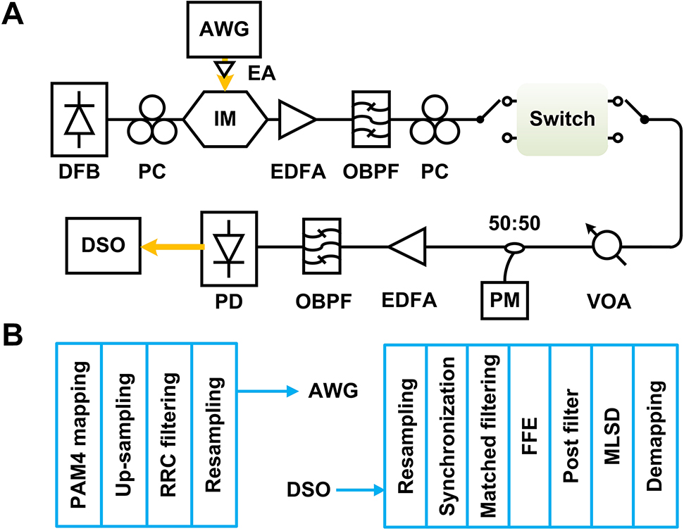
(A) Experimental setup and (B) digital signal processing (DSP) flow charts for the high data rate switching of the device. PM, power meter.
The receiver consists of an EDFA for preamplification, an OBPF, a 50-GHz photodetector (PD), and an 80-GSa/s digital storage oscilloscope (LeCroy 36Zi-A). In the receiver DSP, the signal is first resampled to a sampling rate of two samples per symbol. After the synchronization and matched filtering, a 201-tap linear feedforward equalizer (FFE) is applied. The equalizer coefficients are extracted from the training sequence using recursive least square (RLS) algorithm. To minimize the influence of the noise enhancement effect of the FFE, a 2-tap poster filter and the maximum-likelihood sequence decision are implemented. Finally, the PAM-4 demapping and BER calculation are performed.
Figure 10(A) shows the BER performance of the 62-GBaud PAM-4 signal in the presence of optical switching. The 7% hard-decision forward error correction threshold of 3.8 × 10⁻³ is achieved for all the switching configurations (I1–O1, I1–O2, I2–O1, I2–O2). We also measured the BER curves for the worst switching state (I1–O2) as shown in Figure 10(B). Compared to the optical back-to-back (OBTB) sensitivity of −18.5 dBm, a low penalty of 0.5 dB is observed for the switching signal, indicating the bandwidth of the proposed switch is wide enough for the high-capacity switching at 124 Gb/s rate. The eye diagrams of the recovered PAM-4 signals at different switching configurations are provided in Figure 10(C).
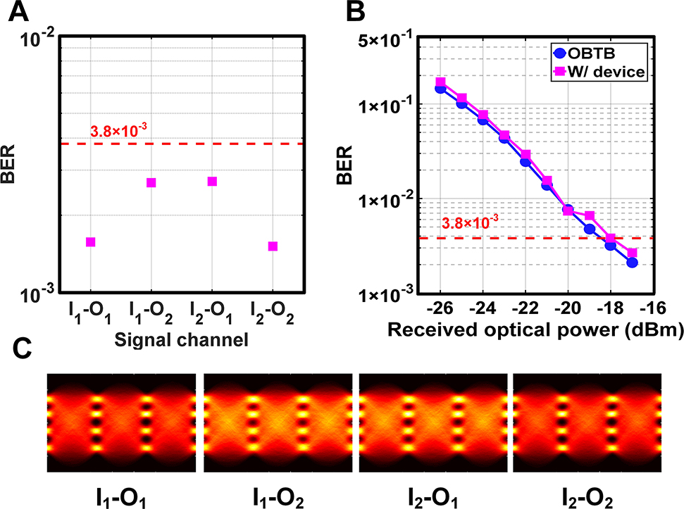
Experimental results for the high data rate switching of the device.
(A) Bit error ratio (BERs) of four switching configurations. (B) BER versus received optical power. (C) Eye diagrams for the four switching configurations of the switch.
6 Summary
In summary, we proposed an optimization method for the designing of a TO switch with a detailed mathematical derivation of the TO tuning process. A suspended PCN-based silicon TO MZI switch is designed to verify the feasibility of the method. Both the simulation and experimental results show significant improvement of the device performance compared with the conventional counterparts. The device is fabricated on a SOI platform with a small footprint of 60 μm × 16 μm. By thermally tuning the refractive index of the silicon PCN waveguides, the cross and bar states of the device can be switched. Only about 0.15 mW tuning power is required for the cross-to-bar switching. Both ILs and cross talk values of the cross and bar state are measured as IL (bar) = 2.0 dB, IL (cross) = 4.4 dB, cross talk (bar) = −13.8 dB, cross talk (cross) = −13.5 dB, at the resonance wavelength of 1560.90 nm. The thermal tuning efficiency of the switch is 7.71 nm/mW. The FWHM is measured as 0.68 nm (i.e. 85 GHz) at the through port with a calculated Q-factor of 2300. Moreover, system performance of high-speed data switching is also studied, which exhibits a low power penalty of less than 0.5 dB at a 124 Gb/s raw data rate with the PAM-4 format.
Funding source: National Natural Science Foundation of China
Award Identifier / Grant number: 61860206001/61835008
Funding source: Shanghai Jiao Tong University
Acknowledgments
The authors acknowledge the support of device fabrication by the Center for Advanced Electronic Materials and Devices (AEMD) of Shanghai Jiao Tong University (SJTU).
-
Author contribution: All the authors have accepted responsibility for the entire content of this submitted manuscript and approved submission.
-
Research funding: National Natural Science Foundation of China (NSFC) (Grant No. 61860206001/61835008).
-
Conflict of interest statement: The authors declare no conflicts of interest regarding this article.
References
[1] M. Asghari and A. V. Krishnamoorthy, “Silicon photonics: energy-efficient communication,” Nat. Photonics, vol. 5, pp. 268–270, 2001.10.1038/nphoton.2011.68Suche in Google Scholar
[2] R. Soref, “Tutorial: integrated-photonic switching structures,” APL Photonics, vol. 3, p. 021101, 2018.10.1063/1.5017968Suche in Google Scholar
[3] Z. Zhou, B. Yin, Q. Deng, X. Li, and J. Cui, “Lowering the energy consumption in silicon photonic devices and systems,” Photon. Res., vol. 3, pp. B28–B46, 2015. https://doi.org/10.1364/prj.3.000b28.Suche in Google Scholar
[4] J. Wang, H. Shen, F. Li, et al.., “Reconfigurable radio-frequency arbitrary waveforms synthesized in a silicon photonic chip,” Nat. Commun., vol. 6, p. 5957, 2015. https://doi.org/10.1038/ncomms6957.Suche in Google Scholar PubMed PubMed Central
[5] S. Yan, X. Zhu, L. H. Frandsen, et al.., “Slow-light-enhanced energy efficiency for graphene microheater on silicon photonic crystal waveguides,” Nat. Commun., vol. 8, p. 14411, 2017. https://doi.org/10.1038/ncomms14411.Suche in Google Scholar PubMed PubMed Central
[6] B. Stern, X. Zhu, C. P. Chen, et al.., “On-chip mode-division multiplexing switch,” Optica, vol. 2, pp. 530–535, 2015. https://doi.org/10.1364/optica.2.000530.Suche in Google Scholar
[7] L. Yang, T. Zhou, H. Jia, et al.., “General architectures for on-chip optical space and mode switching,” Optica, vol. 5, pp. 180–187, 2018. https://doi.org/10.1364/optica.5.000180.Suche in Google Scholar
[8] M. Harjanne, M. Kapulainen, T. Aalto, and P. Heimala, “Sub-μs switching time in silicon-on-insulator Mach–Zehnder thermooptic switch,” IEEE Photonics Technol. Lett., vol. 16, pp. 2039–2041, 2004. https://doi.org/10.1109/lpt.2004.833896.Suche in Google Scholar
[9] I. Kiyat, A. Aydinli, and N. Dagli, “Low-power thermooptical tuning of SOI resonator switch,” IEEE Photonics Technol. Lett., vol. 18, pp. 364–366, 2006. https://doi.org/10.1109/lpt.2005.861951.Suche in Google Scholar
[10] Y. Shoji, K. Kintaka, S. Suda, H. Kawashima, T. Hasama, and H. Ishikawa, “Low-crosstalk 2 × 2 thermo-optic switch with silicon wire waveguides,” Opt. Express, vol. 18, pp. 9071–9075, 2010. https://doi.org/10.1364/oe.18.009071.Suche in Google Scholar PubMed
[11] M. R. Watts, J. Sun, D. R. Christopher, D. C. Trotter, R. W. Young, and G. N. Nielson, “Adiabatic thermo-optic Mach–Zehnder switch,” Opt. Lett., vol. 38, pp. 733–735, 2013. https://doi.org/10.1364/ol.38.000733.Suche in Google Scholar
[12] P. Dong, W. Qian, H. Liang, et al.., “Low power and compact reconfigurable multiplexing devices based on silicon microring resonators,” Opt. Express, vol. 18, pp. 9852–9858, 2010. https://doi.org/10.1364/oe.18.009852.Suche in Google Scholar
[13] P. Sun and R. M. Reano, “Submilliwatt thermo-optic switches using free-standing silicon-on-insulator strip waveguides,” Opt. Express, vol. 18, pp. 8406–8411, 2010. https://doi.org/10.1364/oe.18.008406.Suche in Google Scholar PubMed
[14] Q. Fang, J. Song, T. Y. Liow, et al.., “Ultralow power silicon photonics thermo-optic switch with suspended phase arms,” IEEE Photonics Technol. Lett., vol. 23, pp. 525–527, 2011. https://doi.org/10.1109/lpt.2011.2114336.Suche in Google Scholar
[15] Z. Lu, K. Murray, H. Jayatilleka, and L. Chrostowski, “Michelson interferometer thermo-optic switch on SOI with a 50-μW power consumption,” IEEE Photonics Technol. Lett., vol. 27, pp. 2319–2322, 2015.10.1109/IPCon.2016.7831002Suche in Google Scholar
[16] K. Chen, F. Duan, and Y. Yu, “Performance-enhanced silicon thermo-optic Mach–Zehnder switch using laterally supported suspended phase arms and efficient electrodes,” Opt. Lett., vol. 44, pp. 951–954, 2019. https://doi.org/10.1364/ol.44.000951.Suche in Google Scholar
[17] Y. Zhang, R. Zhang, Q. Zhu, Y. Yuan, and Y. Su, “Architecture and devices for silicon photonic switching in wavelength, polarization and mode,” IEEE/OSA J. Lightwave Technol., vol. 38, pp. 215–225, 2020. https://doi.org/10.1109/jlt.2019.2946171.Suche in Google Scholar
[18] A. M. Al-Hetar, A. B. Mohammad, A. S. M. Supa’At, and Z. M. Shamsan, “MMI-MZI polymer thermo-optic switch with a high refractive index contrast,” IEEE/OSA J. Lightwave Technol., vol. 29, pp. 171–178, 2011. https://doi.org/10.1109/jlt.2010.2098473.Suche in Google Scholar
[19] H. Zhou, C. Qiu, X. Jiang, et al.., “Compact, submilliwatt, 2 × 2 silicon thermo-optic switch based on photonic crystal nanobeam cavities,” Photon. Res., vol. 5, pp. 108–112, 2017. https://doi.org/10.1364/prj.5.000108.Suche in Google Scholar
[20] M. Soljacic and J. D. Joannopoulos, “Enhancement of nonlinear effects using photonic crystals,” Nat. Mater., vol. 3, pp. 211–219, 2004.10.1038/nmat1097Suche in Google Scholar PubMed
[21] J. Zhang and S. He, “Cladding-free efficiently tunable nanobeam cavity with nanotentacles,” Opt. Express, vol. 25, pp. 12541–12551, 2017. https://doi.org/10.1364/oe.25.012541.Suche in Google Scholar
[22] S. E. Mun, C. Choi, J. Hong, and B. Lee, “Broadband wavelength demultiplexer using Fano-resonant metasurface,” Nanophotonics, vol. 5, pp. 1–8, 2020.10.1515/nanoph-2019-0492Suche in Google Scholar
[23] S. G. Johnson, M. Ibanescu, M. A. Skorobogatiy, O. Weisberg, J. D. Joannopoulos, and Y. Fink, “Perturbation theory for Maxwell’s equations with shifting material boundaries,” Phys. Rev. E., vol. 65, p. 066611, 2002. https://doi.org/10.1103/physreve.65.066611.Suche in Google Scholar PubMed
[24] J. D. Joannopoulos, S. G. Johnson, J. N. Winn, and R. D. Meade, Photonic Crystals: Molding the Flow of Light, Princeton, New Jersey, USA, Princeton University Press, 2008.Suche in Google Scholar
[25] Q. M. Quan and M. Loncar, “Deterministic design of wavelength scale, ultra-high Q photonic crystal nanobeam cavities,” Opt. Express, vol. 19, pp. 18529–18542, 2011. https://doi.org/10.1364/oe.19.018529.Suche in Google Scholar
[26] P. B. Deotare, M. W. McCutcheon, I. W. Frank, M. Khan, and M. Loncar, “High quality factor photonic crystal nanobeam cavities,” Appl. Phys. Lett., vol. 94, p. 121106, 2009. https://doi.org/10.1063/1.3107263.Suche in Google Scholar
[27] Y. Zhang, Y. He, Q. Zhu, et al.., “Single-resonance silicon nanobeam filter with an ultra-high thermo-optic tuning efficiency over a wide continuous tuning range,” Opt. Lett., vol. 43, pp. 4518–4521, 2018. https://doi.org/10.1364/ol.43.004518.Suche in Google Scholar
[28] Y. Su, Y. Zhang, C. Qiu, X. Guo, and L. Sun, “Silicon photonic platform for passive waveguide devices: materials, fabrication, and applications,” Adv. Mater. Technol., vol. 1901153, pp. 1–19, 2020.10.1002/admt.201901153Suche in Google Scholar
[29] J. R. Hendrickson, R. Soref, and R. Gibson, “Improved 2 × 2 Mach–Zehnder switching using coupled-resonator photonic-crystal nanobeams,” Opt. Lett., vol. 43, pp. 287–290, 2018. https://doi.org/10.1364/ol.43.000287.Suche in Google Scholar
[30] K. Suzuki, G. Cong, K. Tanizawa, et al.., “Ultra-high-extinction-ratio 2 × 2 silicon optical switch with variable splitter,” Opt. Express, vol. 23, pp. 9086–9092, 2015. https://doi.org/10.1364/oe.23.009086.Suche in Google Scholar PubMed
[31] K. J. Miller, K. A. Hallman, R. F. Haglund, et al.., “Silicon waveguide optical switch with embedded phase change material,” Opt. Express, vol. 25, pp. 26527–26536, 2017. https://doi.org/10.1364/oe.25.026527.Suche in Google Scholar PubMed
[32] Y. Huang, Q. Cheng, Y. Hung, et al., “Dual-microring resonator based 8 × 8 silicon photonic switch,” in Optical Fiber Communication Conference (OFC) 2019, OSA Technical Digest (Optical Society of America), 2019, paper W1E.6.10.1364/OFC.2019.W1E.6Suche in Google Scholar
[33] H. Zheng, M. Grégory, C. Xavier, et al., “High-performance and power-efficient 2 × 2 optical switch on silicon-on-insulator,” Opt. Express, vol. 23, pp. 24163–24170, 2015.10.1364/OE.23.024163Suche in Google Scholar PubMed
Supplementary Material
The online version of this article offers supplementary material (https://doi.org/10.1515/nanoph-2020-0496).
© 2020 Ruihuan Zhang et al., published by De Gruyter, Berlin/Boston
This work is licensed under the Creative Commons Attribution 4.0 International License.
Artikel in diesem Heft
- Reviews
- Carbon nanotube mode-locked fiber lasers: recent progress and perspectives
- In situ charge carrier dynamics of semiconductor nanostructures for advanced photoelectrochemical and photocatalytic applications
- Ligand-induced chirality and optical activity in semiconductor nanocrystals: theory and applications
- Nanostructured inorganic electrochromic materials for light applications
- Temporally modulated energy shuffling in highly interconnected nanosystems
- Recent advances in fluorescence probes based on carbon dots for sensing and speciation of heavy metals
- Research Articles
- Large-scale, power-efficient Au/VO2 active metasurfaces for ultrafast optical modulation
- Near-zero reflection of all-dielectric structural coloration enabling polarization-sensitive optical encryption with enhanced switchability
- Passive photonic diodes based on natural van der Waals heterostructures
- Ultracompact and low-power-consumption silicon thermo-optic switch for high-speed data
- Near-infrared dual-wavelength plasmonic switching and digital metasurface unveiled by plasmonic Fano resonance
- Surface plasmon polariton pulse shaping via two-dimensional Bragg grating pairs
- Subwavelength sorting of full-color based on anti-Hermitian metasurfaces
- Surface plasmon polariton–enhanced photoluminescence of monolayer MoS2 on suspended periodic metallic structures