In situ charge carrier dynamics of semiconductor nanostructures for advanced photoelectrochemical and photocatalytic applications
-
Ting-Hsuan Lai


Abstract
Using in situ ultrafast laser spectroscopic techniques to monitor the charge dynamics of semiconductor photocatalysts under operating conditions is essential for digging out the veritable interactions between charge carriers and the reactive species. This real-time observation is desirable for optimizing individual components and their integration in advanced photoelectrochemical (PEC) and photocatalytic systems, which can achieve the “Holy Grail” of solar energy harvesting and solar fuel generation. This Review summarizes the recent developments of employing transient absorption spectroscopy for in situ measurements of charge dynamics on semiconductor nanostructures. The implications in the PEC and photocatalytic reactions toward hydrogen production and carbon dioxide reduction will be discussed, along with future outlooks and perspectives.
1 Introduction
Over the past few decades, hundreds of thousands of accomplished scientists have dedicated themselves to finding a better energy source that can replace fossil fuels. Plenty of strategies toward the development of clean, sustainable energy resources have been proposed and realized, such as solar heat collection [1], [ 2], thermoelectric conversion [3], [ 4], photovoltaics [5], [ 6], water electrolysis [7], [ 8], solar hydrogen production [9], [ 10], and carbon dioxide reduction [11], [ 12]. A reliable and sustainable alternative energy source must be realized to avoid a serious energy crisis in coming decades. Among all the strategies reported, hydrogen energy is one of the most promising alternative energies. Several advantages, such as a high heat value [13], elemental abundance, and nontoxicity, have brought substantial attention to this carbon-free energy. Two solar-to-hydrogen pathways have been proposed and studied for decades, including photoelectrochemical (PEC) [14] and photocatalytic water splitting [15]. In these systems, specific semiconductor nanostructures are selected as photoelectrodes and photocatalysts and brought into contact with water molecules under solar light irradiation, dissociating water into hydrogen and oxygen. This system is cost-effective and simple for both laboratory and industrial production scales. In addition to hydrogen production, the reduction of carbon dioxide into solar fuels in PEC [16] and photocatalytic [17] processes has also triggered an ever-increasing interest. This approach focuses on converting greenhouse gases into valuable chemicals, opening a new era of storing renewable energy in chemicals. Research on the conversion and storage of solar energy in terms of hydrogen or carbon-based fuels offers great potential for solving the sustainable energy challenge.
PEC systems are a viable platform for solar energy conversion. The PEC cell is inspired by the traditional electrochemical cell, in which solar energy and electrochemical bias collaborate to drive the desired redox reactions on the selected semiconductor photoelectrodes. With the help of an electrochemical bias, solar energy can be efficiently utilized, converted, and stored in another chemical form. Photocatalysts, in the form of particular nanostructures, are often used in a photocatalytic system in order to maximize the available catalytically active sites. Despite the low solar-to-fuel efficiency that is often reported [18], [19], [20], photocatalytic hydrogen production and carbon dioxide reduction are still feasible, and represent cost-effective solutions to meet the global energy demand. In general, single, plain semiconductors without further modifications suffer from pronounced charge carrier recombination due to Coulomb force. Upon photoexcitation, the negatively charged electrons in the conduction band are naturally bound to the positively charged holes in the valence band by the electrostatic Coulomb attraction [21]. For plain semiconductors, the bound electrons and holes are prone to recombination because of the lack of driving force of pulling them apart, limiting their further participation in surface redox reactions. The design and engineering of ingenious materials, such as heterostructure introduction [22], cocatalyst deposition [23] and dopant introduction [24], [25], [26], are thus essential to expediting the charge carrier transfer. If charge carriers survive recombination and live long enough, they can diffuse to the surface of the photoelectrodes and photocatalysts participating in the desired catalytic reactions. Whether the delocalized charge carriers can be effectively separated and injected into the electrolyte dramatically affects the overall PEC and photocatalytic performance. The charge transfer and recombination at the semiconductor surface is a relatively slow process that lies in the microseconds (μs) or even milliseconds (ms) timescale [27], [ 28]. Therefore, charge dynamics at the semiconductor’s surface is the rate-determining step of the surface redox reactions and play a decisive role in the PEC and photocatalytic processes. A thorough analysis and study of the interfacial charge dynamics must be conducted beforehand in an effort to construct the true reaction mechanism for maximizing the solar-to-fuel conversion efficiency. In particular, for carbon dioxide reduction the entire reaction involves multielectron transfer pathways [29], [30], [31], which makes it exceedingly challenging to comprehend. Realizing the real reaction mechanism has thus become indispensable to the widespread deployment of PEC and photocatalytic techniques.
Transient absorption (TA) spectroscopy is a powerful tool for examining the charge transfer events of semiconductor nanostructures [32], [ 33]. Ex situ measurement is a common method for analyzing the charge dynamics properties of semiconductors by TA. During the measurements, the samples are either placed in air or dispersed in a specific solvent (water or ethanol) in order to meet the criteria of the spectroscopic setup. Although much progress has been made, the derived charge transfer scenarios from ex situ TA measurements are often distorted and unreliable because the operating conditions, such as external bias and electrolyte presence, are not considered. To address this issue, real-time investigation of charge dynamics via in situ TA experiments has drawn increasing attention. Important experimental factors, such as the application of electrochemical bias, the use of electrolytes and the concurrent occurrence of surface redox reactions, can be addressed by in situ measurements. In this Review, we summarize the recent progress of employing in situ TA spectroscopy when studying the interfacial charge dynamics of semiconductor nanostructures for hydrogen production and carbon dioxide reduction. As depicted in Scheme 1, representative research works that report the real-time charge dynamics of photoelectrodes and photocatalysts by conducting in situ TA measurements will be introduced. The content of this Review is divided into four parts. In the first part, we introduce the basic principle of employing TA spectroscopy when analyzing the charge dynamics of semiconductor nanostructures. Following that, previous studies on representative photoelectrodes (TiO2, BiVO4, WO3, α-Fe2O3) and photocatalysts (Cu2O, TiO2) are reviewed. Perspectives on the future directions for real-time charge dynamics of photoelectrodes and photocatalysts are provided at the end of the Review.
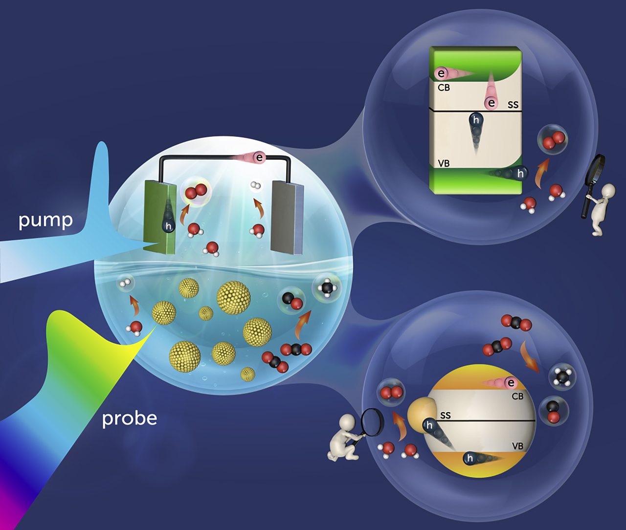
Illustrations of employing in situ transient absorption (TA) spectroscopy to elucidate the veritable charge dynamics scenarios for semiconductor photoelectrodes and photocatalysts.
2 TA spectroscopy
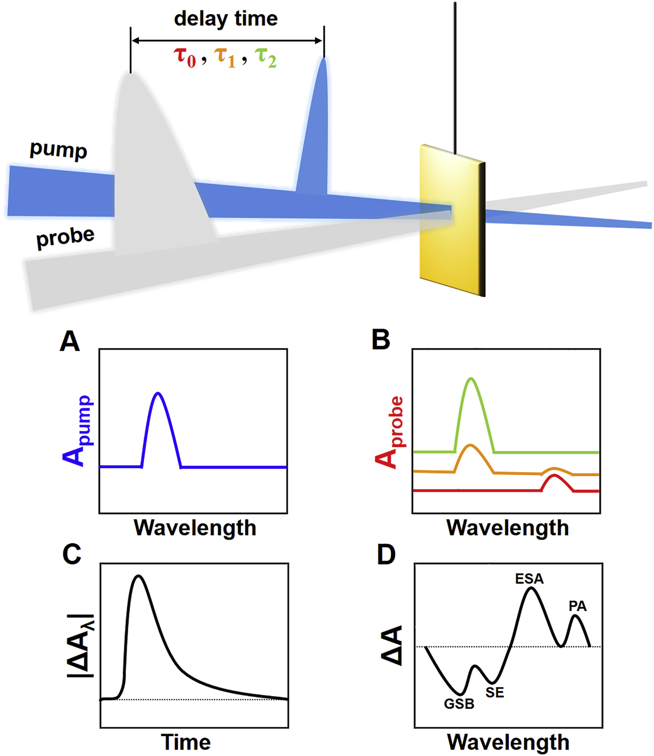
TA spectroscopy is a typical pump–probe spectroscopic technique, which measures the temporal absorption changes of the samples before and after excitation [34]. A basic setup of TA spectroscopy is composed of an ultrafast monochromatic laser excitation, a low-energy broadband probing light and a spectrometer recording the absorbance of the samples [35]. The samples are first excited by an ultrafast fs pump laser. The duration of laser pulse should be carefully tuned to produce a suitable spectral width for studying specific excited state dynamics. After a certain amount of time, the absorbance of the samples is measured by a second probe beam. This probe beam usually ranges from 400 to 1000 nm and should be weak enough to avoid any multiphoton processes. By introducing a time variable, the absorbance variation profile over time can be collected and analyzed. As illustrated in Figure 1, the difference in the absorption spectrum (ΔA) is obtained by subtracting the absorption spectrum of the samples at the ground state (A pump, Figure 1A) from the absorption spectrum collected at the excited state (A probe, Figure 1B), i.e. ΔA = A probe − A pump. The spectrum of ΔA as a function of delay time (τ) and wavelength (λ) can be collected by tuning the delay time between the pump laser and probe beam (Figure 1C). Two types of spectroscopic profiles can be derived from the three-dimensional contour data, including a single-wavelength and a single-time point analysis. The single-wavelength profile can be interpreted to describe the excited states’ deactivation processes, such as electron–hole recombination, interfacial charge transfer, charge trapping, etc. First-order trap state-mediated recombination and second-order free carrier recombination kinetics models can be used to analyze these kinetics processes both systematically and quantitatively. On the other hand, the single-time profile provides quantitative information of excited states’ deactivation in a selected timeframe. Direct comparison of the variance of carrier concentration in a specific pathway is possible by simply evaluating the amplitude contribution of the TA component. There are four probable mechanisms accountable for different ΔA behaviors, which include ground state bleaching (GSB), stimulated emission (SE), excited state absorption (ESA) and product absorption (PA) [35], [ 36]. As displayed in Figure 1D, GSB originates from the reduced number of charge carriers in the ground state for the excited samples. In other words, the absorbance of the excited samples (A probe) is lower than the absorbance of the nonexcited samples (A pump), producing negative signals in the ΔA spectrum. SE refers to a two-level process, in which the photons of the probing light interact with the excited electrons, inducing an emission of additional photons with the spectral feature following the fluorescence of the samples. This transition causes an increase in transmitted intensity recorded by the detector, giving an intrinsically negative absorbance (A probe < 0). Because SE only occurs in the excited state, the corresponding ground state absorption is supposed to be approaching zero (A pump = 0), leading to negative ΔA signals in the TA profile. ESA on the other hand describes the charge carrier relaxation from the excited state to the higher excited state upon photoexcitation. Since only probing light is absorbed (A probe > 0 and A pump = 0), positive ΔA signals are expected in the TA profile. Similar to ESA, PA represents specific electronic transition processes that only take place upon photoexcitation. Long-lived charge transfer events associated with triplet states, charge separation and isomeric transition are possible causes. Absorption of these events by probing light then appears as positive ΔA in the TA profile. TA spectroscopy allows us to monitor the charge carrier dynamics within semiconductor nanostructures by means of spectroscopic characterization. A thorough understanding of the photophysics beyond the collected TA data is essential for interpreting the interfacial charge dynamics of semiconductor nanostructures.
Basic mechanism of transient absorption (TA) spectroscopy.
(A) ground state absorption spectrum, (B) excited state absorption spectrum, (C) TA profile probed at a specific wavelength, (D) four possible mechanisms contributing to the recorded TA signals.
3 PEC systems
Charge carrier dynamics of semiconductor nanostructures in PEC systems have been studied and reported with the help of in situ TA spectroscopy. Several common semiconductor materials have been used as photoelectrodes when studying in situ TA, including TiO2 photoanodes [37], [38], [39], [40], BiVO4 photoanodes [41], [ 42], WO3 photoanodes [43], [44], [45], α-Fe2O3 photoanodes [46], [47], [48], [49], [50], and ZnTe photocathodes [51]. In this section, we introduce several representative works to highlight the importance of using in situ TA spectroscopy toward the realization of interfacial charge dynamics for photoelectrodes under operating conditions.
3.1 TiO2 photoanodes
Since the first report of the photoactivity property of TiO2 by Fujishima and Honda [52], this photoelectrode archetype has been thoroughly studied over the past few decades. TiO2 photoelectrodes have several advantages, such as having a high stability, a low cost, and being environmental-friendly. Therefore, TiO2 has been widely used in various PEC applications, including PEC water splitting [53], [54], [55], [56], [57], [58], PEC fuel cells [59], PEC dye degradation [60], [61], [62] and PEC sensing [63], [64], [65], [66]. Cowan et al. reported the charge carrier dynamics within a TiO2 photoanode under PEC operating conditions [38]. Nanocrystalline rutile TiO2 films (nc-TiO2) were deposited on the conductive fluorine-doped tin oxide substrate. A linear-sweep voltammetry measurement revealed that the onset potential of anodic photocurrent was approximately −0.8 V (vs. Ag/AgCl). The photocurrent reached a saturated value of 50 μA at −0.5 V. In situ TA spectroscopy was used to quantitatively analyze the carrier dynamics, providing a better understanding of charge transfer scenarios during the PEC reaction. In Figure 2A, the TA data were collected at 10 μs and 5 ms after the excitation of a 355 nm UV light (pump) at −0.9 and 0 V. At −0.9 V (a potential less anodic than the onset potential), a broad featureless absorption decay within a 10 μs to 5 ms timescale was observed. Under UV excitation, the absorption band of the photoholes and trapped photoelectrons were located at 450 [67], [ 68] and 770 nm [69], respectively. Therefore, the overlapped absorption of the photoholes and trapped photoelectrons led to the broad featureless absorption decay. However, at a largely anodic bias (0 V), a strong absorption band around 460 nm was found, which could be attributed to the long-lived photoholes. A similar spectral feature attributable to the photoholes was also observed on platinized nc-TiO2 (Pt-nc-TiO2) [70]. This absorption can still be observed at 5 ms after the UV excitation. In contrast, the absorption of trapped photoelectrons around 800 nm completely decayed within 5 ms after UV excitation. In Figure 2B, the decay profile was probed at 460 nm at 0 V. This decay profile can be fitted by two decay components: (1) power law decay and (2) stretched exponential decay. The fast component (1) can be attributed to electron–hole recombination, while the slow component (2) can be assigned to the oxidation reaction between photoholes and water at the photoelectrode surface. The slow component has a lifetime of 30 ms, suggesting that the formation of long-lived photoholes is a prerequisite for the water splitting reaction [71]. From the inset of Figure 2B, the TA profile of the photoholes showed a longer lifetime than the profile of the trapped photoelectrons. Meanwhile, the profile of the trapped photoelectrons was highly similar to the fast decay component of the TA profile of photoholes. Therefore, it can be concluded that the early stage of photoholes absorption is dominated by electron–hole recombination, and the oxidation reaction between photoholes and water contributes to the late stage of the decay profile. In Figure 2C, the absorption of trapped photoelectrons gradually increased when the applied bias was anodically shifted from −0.9 to 0 V. The electron density in the interband trap states decreased under a more anodic bias condition, and this decrease contributed to the prolonged lifetime of the trapped photoelectrons. The decay profiles of photoholes were also recorded under different applied biases. As shown in Figure 2D, these profiles again displayed two decay components. At a potential more anodic than −0.5 V, no appreciable change in the TA profile of photoholes could be found. This feature was consistent with the observed photocurrent saturation at −0.5 V. Noticeably, the electron–hole recombination (fast component) showed a decreased rate at a more anodic bias. This would result in a larger proportion of photoholes that could react with water, therefore enhancing the overall water oxidation efficiency. Figure 2E depicts the plausible charge dynamics pathways for an nc-TiO2 photoanode. After UV excitation, the photoholes would either recombine with the trapped photoelectrons or live long enough to react with water. Under an anodic bias condition, the trapped photoelectrons would be detrapped and transfer to the counter electrode, preventing them from recombining with photoholes. Meanwhile, the remaining photoholes would further react with the water, undergoing a water oxidation reaction.
![Figure 2:
(A) In situ transient absorption (TA) spectra of nc-TiO2 recorded at −0.9 and 0 V in 0.05 M NaOH at 10 μs and 5 ms after UV excitation (355 nm, 250 μJ cm−2). The Pt-nc-TiO2 spectrum was adopted from the literature [70]. (B) TA profile of the photoholes (460 nm) at 0 V. Inset highlights the difference in the TA profile between the photoholes (460 nm) and trapped photoelectrons (800 nm). (C–D) TA profiles of trapped photoelectrons (C panel) and photoholes (D panel) under different applied biases. (E) Proposed charge dynamics mechanism of nc-TiO2. Reprinted with permission from a study by Cowan et al. [38]. Copyright 2010 American Chemical Society. (F) TA profile of photoholes for nc-TiO2 (460 nm) at 0 V in 0.5 M NaClO4 under UV excitation (355 nm, 35 μJ cm−2) and its correlation with the fractional yield of photoholes. (G) TA profiles of photoholes under different applied biases. (H) Correlation of the two η
sep values derived from incident photon-to-current conversion efficiency (IPCE) and TA measurements with the applied bias under UV excitation (355 nm and 3.7 mW cm−2 for IPCE; 355 nm and 35 μJ cm−2 for TA). Reprinted with permission from a study by Cowan et al. [40]. Copyright 2013 Royal Society of Chemistry.](/document/doi/10.1515/nanoph-2020-0472/asset/graphic/j_nanoph-2020-0472_fig_002.jpg)
(A) In situ transient absorption (TA) spectra of nc-TiO2 recorded at −0.9 and 0 V in 0.05 M NaOH at 10 μs and 5 ms after UV excitation (355 nm, 250 μJ cm−2). The Pt-nc-TiO2 spectrum was adopted from the literature [70]. (B) TA profile of the photoholes (460 nm) at 0 V. Inset highlights the difference in the TA profile between the photoholes (460 nm) and trapped photoelectrons (800 nm). (C–D) TA profiles of trapped photoelectrons (C panel) and photoholes (D panel) under different applied biases. (E) Proposed charge dynamics mechanism of nc-TiO2. Reprinted with permission from a study by Cowan et al. [38]. Copyright 2010 American Chemical Society. (F) TA profile of photoholes for nc-TiO2 (460 nm) at 0 V in 0.5 M NaClO4 under UV excitation (355 nm, 35 μJ cm−2) and its correlation with the fractional yield of photoholes. (G) TA profiles of photoholes under different applied biases. (H) Correlation of the two η sep values derived from incident photon-to-current conversion efficiency (IPCE) and TA measurements with the applied bias under UV excitation (355 nm and 3.7 mW cm−2 for IPCE; 355 nm and 35 μJ cm−2 for TA). Reprinted with permission from a study by Cowan et al. [40]. Copyright 2013 Royal Society of Chemistry.
Another study conducted by Cowan et al. researched the reasons for the low incident photon-to-current conversion efficiency (IPCE) of nc-TiO2 by analyzing the in situ TA data [40]. An equation commonly used to evaluate the factors affecting IPCE value can be shown by
In order to enhance the PEC performance of TiO2, numerous strategies have been reported, such as foreigner element doping [55], [ 73], metal particle deposition [53], [ 56], type-II/Z-scheme heterojunction introduction [54], [57], [74], and photosensitizer incorporation [75], [ 76]. Pesci et al. studied oxygen-deficient, hydrogen-treated rutile TiO2 (H:TiO2) nanowire photoanodes [39] and conducted in situ TA measurements under various biases to establish a plausible charge dynamics mechanism. Figure 3A shows the band structure of air-annealed (A:TiO2) and H:TiO2. After the hydrogen treatment, the concentration of oxygen vacancies (VO) increases. Note that the energetic states of VO lie within the bandgap, which are around 0.75 and 1.18 V below the conduction band edge. These VO states can serve as electron donors (EDs) to increase the carrier concentration. In the PEC system under an applied bias, the increased donor concentration can also assist in suppressing electron–hole recombination because the photovoltage drop across the depletion layer is greatly enhanced. In Figure 3B, the linear-sweep voltammograms are in a good agreement with the TA amplitude change probed at 500 nm and 10 ms after excitation under various biases. Since photoholes play a decisive role in the water oxidation activity, the results of Figure 3B further validate that the TA signals in the 425–550 nm region were contributed to by the photohole dynamics of rutile TiO2. Figure 3C compares the in situ TA profiles between H:TiO2 and A:TiO2. At −0.85 V (vs. Ag/AgCl), both H:TiO2 and A:TiO2 showed power law decay kinetics with a short carrier lifetime and indistinguishable kinetics profiles for the photoholes (500 nm) and trapped photoelectrons (800 nm) at the ms–sec timescale. This feature is characteristic of the pronounced electron–hole recombination. As the applied bias shifts anodically to −0.6 V, there is a relatively large increase in the absorbance for H:TiO2 at the early timescale (1–10 µs). Such an absorbance increase reflects an increased yield of photoelectrons and photoholes, indicating the suppression of fast recombination under an anodic bias. In contrast, A:TiO2 shows a minimal change in the charge carrier yield as the applied bias is anodically varied. This outcome suggests that the early charge separation process is essential to enhancing the photoactivity of H:TiO2. Another conspicuous feature from Figure 3C is that the decay kinetics of photoelectrons and photoholes are decoupled at the ms–sec timescale. This observation indicates that processes other than electron–hole recombination can occur under anodic bias conditions. In Figure 3D, the TA profiles of photoholes (500 nm) and trapped photoelectrons (800 nm) at −0.6 V for H:TiO2 and A:TiO2 are compared. For H:TiO2, the trapped photoelectrons decay by more than 50% in the early stage (10 μs to 1 ms), whereas the photoholes remain almost unchanged at the same timescale. The fast decay of trapped photoelectrons follows a power law kinetics model (τ = 14 ms) and is attributed to the electron transfer to the external circuit. However, the slow decay of photoholes can be well fitted with a single stretched exponential function (τ = 0.15 s) and is assigned to the hole injection into the electrolyte. This timescale is at the same magnitude with the photohole lifetime (τ = 0.03–0.4 s) required for effective water oxidation on anatase TiO2 photoelectrodes [77]. Conversely, on A:TiO2, the photohole decay profile at −0.6 V can be fitted by a combination of stretched exponential and power law functions, implying there are at least two probable photohole transfer pathways. The fast decay component is assigned to electron–hole recombination, whereas the slow decay component is attributed to a photohole injection into the solution. These two events compete with one another and deteriorate the water oxidation activity.
![Figure 3:
(A) Proposed charge dynamics mechanism of A:TiO2 and H:TiO2 at an anodic bias after UV excitation. k
ct, k
r and k
et respectively stand for the rate constants of the charge transfer into the solution, the charge recombination, and the electron transfer. E
1O and E
2O respectively denote the two states of VO at 0.75 and 1.2 eV below the conduction band edge. (B) Linear-sweep voltammograms and in situ transient absorption (TA) amplitude change at 500 nm and 10 ms after UV excitation (λ = 355 nm, 70 μJ cm−2) for A:TiO2 and H:TiO2 in 1 M NaOH under various applied biases. (C) TA profiles of A:TiO2 and H:TiO2 at different applied biases. (D) TA decay profiles of photoholes (500 nm) and trapped photoelectrons (800 nm) for H:TiO2 and A:TiO2 at −0.6 V. Reprinted with permission from a study by Pesci et al. [39]. Copyright 2013 American Chemical Society.](/document/doi/10.1515/nanoph-2020-0472/asset/graphic/j_nanoph-2020-0472_fig_003.jpg)
(A) Proposed charge dynamics mechanism of A:TiO2 and H:TiO2 at an anodic bias after UV excitation. k ct, k r and k et respectively stand for the rate constants of the charge transfer into the solution, the charge recombination, and the electron transfer. E 1O and E 2O respectively denote the two states of VO at 0.75 and 1.2 eV below the conduction band edge. (B) Linear-sweep voltammograms and in situ transient absorption (TA) amplitude change at 500 nm and 10 ms after UV excitation (λ = 355 nm, 70 μJ cm−2) for A:TiO2 and H:TiO2 in 1 M NaOH under various applied biases. (C) TA profiles of A:TiO2 and H:TiO2 at different applied biases. (D) TA decay profiles of photoholes (500 nm) and trapped photoelectrons (800 nm) for H:TiO2 and A:TiO2 at −0.6 V. Reprinted with permission from a study by Pesci et al. [39]. Copyright 2013 American Chemical Society.
3.2 BiVO4 photoanodes
BiVO4 is an n-type semiconductor with a narrow bandgap (E
g = 2.4 eV) that is suitable for visible light absorption. In addition, the relatively cathodic valence band edge (E
VB = +2.5 V vs. NHE) [78] is able to drive many oxidation reactions. However, BiVO4 suffers from a short hole diffusion length that makes the overall solar-to-fuel efficiency low. Zhang et al. reported a black phosphorene (BP)–deposited BiVO4 (BP/BiVO4) nanostructure photoanode, in which the BP layer could facilitate photohole extraction as a result of the p–n band alignment, promoting the overall water oxidation efficiency. The morphology of the prepared BiVO4 and BP/BiVO4 nanostructures is revealed in Figure 4A, showing a thickness of approximately 1 µm. In order to elucidate the veritable charge dynamics of BP/BVO, in situ TA measurements were performed. Note that the TA signals of the photoholes of BP/BVO are situated around 400–700 nm [79]. To acquire information on the photohole dynamics, the TA profiles were probed at 500 nm under open-circuit potential (OCP) and 0.8 V (vs. Ag/AgCl). In Figure 4B and C, the collected TA spectra are fitted by a biexponential decay model (
![Figure 4:
(A) SEM images of BiVO4 and black phosphorene (BP)/BiVO4. (B–C) In situ TA profiles of the photoholes (500 nm) for BiVO4 and BP/BiVO4 at OCP (B panel) and 0.8 V (C panel) in 0.5 M KPi. (D) Fitting parameters of the recorded TA profiles. (E) η
sep of BiVO4 and BP/BiVO4 at different applied biases. Reprinted with permission from a study by Zhang et al. [42]. Copyright 2019 Springer Nature.](/document/doi/10.1515/nanoph-2020-0472/asset/graphic/j_nanoph-2020-0472_fig_004.jpg)
(A) SEM images of BiVO4 and black phosphorene (BP)/BiVO4. (B–C) In situ TA profiles of the photoholes (500 nm) for BiVO4 and BP/BiVO4 at OCP (B panel) and 0.8 V (C panel) in 0.5 M KPi. (D) Fitting parameters of the recorded TA profiles. (E) η sep of BiVO4 and BP/BiVO4 at different applied biases. Reprinted with permission from a study by Zhang et al. [42]. Copyright 2019 Springer Nature.
Another strategy for enhancing the solar-to-fuel efficiency of BiVO4 is to introduce a type-II band alignment, which can achieve a pronounced charge carrier separation. WO3-modified BiVO4 (WO3/BiVO4) is a common type-II heterostructure model studied in PEC water splitting systems. The band alignment allows photoelectrons to flow from the BiVO4 to the WO3 domain, leaving the photoholes in the BiVO4 domain to conduct a water oxidation reaction. Selim et al. [80] reported the interfacial charge dynamics of WO3/BiVO4 by using in situ TA spectroscopy. Figure 5A and B shows the TA spectra under 1.23 V (vs. RHE) and OCP at 10 µs and 10 ms after excitation. Note that the samples were excited from the BiVO4 side with the aim of exclusively studying the dynamics of the charge transfer from BiVO4 to WO3. Under 1.23 V, the TA profile of pure BiVO4 exhibits a maximum absorption at 550 nm, whereas the TA profile of WO3/BiVO4 shows an additional absorption band at a long wavelength that disappears by 10 ms. Previous work has shown that the photoelectrons of WO3 exhibit a broad absorption around 800 nm [45], [ 81]. Because WO3 was not excited in the current TA setup, the photoelectron signal of WO3 at a long wavelength region was attributed to the photoelectron transfer from BiVO4 to WO3 at a µs timescale. However, at the OCP there was no noticeable difference in the TA decay between BiVO4 and WO3/BiVO4. Importantly, the lack of a photoelectron signal for WO3/BiVO4 suggested that an applied bias was necessary for prompting the photoelectron transfer from BiVO4 to WO3. In Figure 5C and D, the TA profiles of photoholes (500 nm) of pure BiVO4 and WO3/BiVO4 were compared under different applied biases. These kinetics traces could be fitted with a combination of a power law and a single exponential function. The photohole yield increased with an increasing anodic bias, with WO3/BiVO4 showing a more pronounced enhancement. Note than the anodic bias could create a wider depletion layer at the electrode/electrolyte interface, which increased the band bending to promote photohole accumulation at the photoanode surface. For pure BiVO4, which showed biphasic TA kinetics, two pathways of photohole dynamics were considered: trap-mediated bimolecular recombination at an early timescale (μs–ms) and water oxidation process coupled with back electron–hole recombination at a slow timescale (ms–sec). Compared with BiVO4 (τ = 0.18 s at 1.2 V), WO3/BiVO4 showed an increased lifetime of photoholes (τ = 0.29 s at 1.2 V), demonstrating the suppression of bimolecular recombination by the introduction of WO3. The plausible charge dynamics mechanism is shown in Figure 5E and F. In pure BiVO4, photoholes suffer from bimolecular recombination, and thus the water oxidation performance is limited. With the introduction of WO3, photoelectron transfer from BiVO4 to WO3, prohibiting charge carriers from bimolecular recombination. This results in the formation of long-lived photoholes at BiVO4, which has been considered as a requisite for driving efficient water oxidation on BiVO4 [82].
![Figure 5:
(A, B) In situ transient absorption (TA) spectra of BiVO4 and WO3/BiVO4 at 1.23 V (A panel) and open-circuit potential (OCP) (B panel) in a 0.1 M phosphate buffer recorded at 10 μs and 10 ms after UV excitation (355 nm, 500 μJ cm−2). (C, D) TA profiles of photoholes (500 nm) of BiVO4 and WO3/BiVO4 at different applied biases. (E, F) Proposed charge dynamics mechanism of BiVO4 and WO3/BiVO4, in which (i) represents water oxidation at the BiVO4 surface, (ii) denotes the electron transfer from BiVO4 to WO3 and (iii) stands for the photoelectron extraction from the photoanode to the external circuit. Reprinted with permission from a study by Selim et al. [80] Copyright 2013 Royal Society of Chemistry.](/document/doi/10.1515/nanoph-2020-0472/asset/graphic/j_nanoph-2020-0472_fig_005.jpg)
(A, B) In situ transient absorption (TA) spectra of BiVO4 and WO3/BiVO4 at 1.23 V (A panel) and open-circuit potential (OCP) (B panel) in a 0.1 M phosphate buffer recorded at 10 μs and 10 ms after UV excitation (355 nm, 500 μJ cm−2). (C, D) TA profiles of photoholes (500 nm) of BiVO4 and WO3/BiVO4 at different applied biases. (E, F) Proposed charge dynamics mechanism of BiVO4 and WO3/BiVO4, in which (i) represents water oxidation at the BiVO4 surface, (ii) denotes the electron transfer from BiVO4 to WO3 and (iii) stands for the photoelectron extraction from the photoanode to the external circuit. Reprinted with permission from a study by Selim et al. [80] Copyright 2013 Royal Society of Chemistry.
3.3 WO3 photoanodes
WO3 is another well-reported n-type semiconductor for use as a photoanode in PEC water splitting thanks to the visible light-responsive band structure (E g = 2.5 eV). However, the fast charge recombination at the surface defect sites (W5+ and surface states) hinders the overall PEC performance. Several strategies have been proposed to address this issue, such as hydrogen treatment [83], [ 84], co-catalyst deposition [85], [86], [87] and passivation layer introduction [88], [ 89]. Kim et al. reported an efficient surface passivation approach for decreasing the photoelectron trapping event for WO3 using an Al2O3 overlayer [44]. The photoanode was fabricated by depositing a 5.3-nm-thick Al2O3 layer on WO3 thin films (WO3/Al2O3). The deposited Al2O3 not only promoted photoelectron transfer to the external circuit by passivating the electron traps but also boosted the water oxidation kinetics by arousing the photohole trapping process. The photoelectron trapping event was first examined with a steady-state absorption spectroscopy under two distinct applied biases, one above the photocurrent onset (1.3 V [vs. Ag/AgCl]) and the other one below the photocurrent onset (0 V [vs. Ag/AgCl]). In Figure 6A, the absorbance change at 800 nm of pure WO3 and Al2O3/WO3 was measured under a bias condition. Here, the absorption at 800 nm could be attributed to photoelectron trapping signal of WO3 [90], which remained unchanged at 1.3 V, despite the deposition of Al2O3. However, at 0 V there was a notable absorbance increase indicative of photoelectron accumulation on both pure WO3 and Al2O3/WO3. Importantly, the photoelectron accumulation of WO3 (absorbance at 800 nm) was largely reduced upon the deposition of Al2O3. This result indicates that Al2O3 could passivate the electron traps of WO3 to promote photoelectron transfer to the external circuit. This would further mediate the photohole dynamics of WO3 to affect the overall PEC performance.
![Figure 6:
(A) Absorbance change at 800 nm for pure WO3 and Al2O3/WO3 at different applied biases in Ar-purged 0.1 M HClO4. (B) Transient absorption (TA) profiles of photoholes (480 nm) at open-circuit potential (OCP) and 1.3 V after UV excitation (355 nm, 250 μJ pulse−1). (C) TA spectra of pure WO3 and Al2O3/WO3 at 1.3 V and 2 μs after UV excitation. A, B represents the subtracted spectrum. (D) Proposed charge dynamics mechanism of pure WO3 and Al2O3/WO3 under a bias condition. (E) Deconvoluted TA spectra of pure WO3 and Al2O3/WO3 at 1.3 V and 2 μs after UV excitation. Reprinted with permission from a study by Kim et al. [44]. Copyright 2013 Royal Society of Chemistry.](/document/doi/10.1515/nanoph-2020-0472/asset/graphic/j_nanoph-2020-0472_fig_006.jpg)
(A) Absorbance change at 800 nm for pure WO3 and Al2O3/WO3 at different applied biases in Ar-purged 0.1 M HClO4. (B) Transient absorption (TA) profiles of photoholes (480 nm) at open-circuit potential (OCP) and 1.3 V after UV excitation (355 nm, 250 μJ pulse−1). (C) TA spectra of pure WO3 and Al2O3/WO3 at 1.3 V and 2 μs after UV excitation. A, B represents the subtracted spectrum. (D) Proposed charge dynamics mechanism of pure WO3 and Al2O3/WO3 under a bias condition. (E) Deconvoluted TA spectra of pure WO3 and Al2O3/WO3 at 1.3 V and 2 μs after UV excitation. Reprinted with permission from a study by Kim et al. [44]. Copyright 2013 Royal Society of Chemistry.
In situ TA spectroscopy was further performed to investigate the photohole dynamics. In Figure 6B, the TA profiles of trapped photoholes (480 nm [81]) at OCP and 1.3 V for pure WO3 and Al2O3/WO3 were compared. The yield of the trapped photoholes (i.e., the TA intensity) of Al2O3/WO3 was largely increased at 1.3 V, while the increased photohole yield of pure WO3 was less pronounced. This comparison suggests that Al2O3 passivation can enhance the number of trapped photoholes for WO3. To confirm this argument, the TA spectra of pure WO3 at 1.3 V and 2 µs after UV excitation were subtracted from those of Al2O3/WO3 to reveal the photohole population as a result of the Al2O3 passivation. As Figure 6C shows, the spectral subtraction (A, B) reveals a substantial increase in the photohole trapping signal at 480 nm. This outcome corroborates that the increased photohole trapping also contributed to the better PEC performance of Al2O3/WO3. Figure 6D depicts the proposed charge dynamics mechanism for pure WO3 and Al2O3/WO3. For pure WO3, trapped photoelectrons dominated the charge transfer dynamics to hinder the PEC performance. Upon Al2O3 deposition, the electron traps of WO3 could be passivated, accompanied by an increased population of trapped photoholes, both of which were beneficial for PEC water oxidation. In Figure 6E, the deconvoluted TA spectra could be utilized to quantify the number of trapped photoelectrons and photoholes for pure WO3 and Al2O3/WO3. The trapped photohole population of Al2O3/WO3 was three times higher than that of pure WO3. On the other hand, the number of trapped photoelectrons of Al2O3/WO3 was merely 20% of the number of Al2O3/WO3. This result confirmed the benefit of Al2O3 deposition for enhancing the PEC water oxidation activity of WO3 by mediating interfacial charge dynamics.
3.4 α-Fe2O3 photoanodes
α-Fe2O3 (hematite) is a well-reported promising photoanode material with several advantages. The bandgap of α-Fe2O3 (E g = 2.1 eV) [91] is capable of visible light absorption, and the valence band edge (E VB = +2.38 V vs. NHE) [92], [ 93] is thermodynamically suitable for water oxidation reactions. However, there are several intrinsic properties that deteriorate the solar-to-fuel efficiency of α-Fe2O3. The drawbacks include limited photon harvesting due to the high light penetration depth [94], and the incapability of hydrogen production because of an unfavorable conduction band edge (E CB = +0.28 V vs. NHE) [95], as well as sluggish water oxidation kinetics resulting from a short photohole diffusion [96]. The issue of photohole dynamics is particularly critical, thus invigorating broad interests in studying the charge dynamics of α-Fe2O3. Barroso et al. [47] reported a perspective that summarized the recent studies on interfacial charge dynamics for α-Fe2O3 by employing in situ TA spectroscopy. Figure 7A shows the in situ TA spectra at 800 nm for Si-doped α-Fe2O3 photoanode. Under 0.5 V (vs. RHE) (around the flat-band potential), the spectrum exhibits a positive absorption at 580 nm, which rapidly decays within a few ms due to fast electron–hole recombination. As the applied bias anodically shifts from 0.8 to 1.6 V, the TA lifetime notably increases by three orders of magnitude. A broad, long-lived absorption centered at approximately 650 nm and a narrow, negative bleaching at 580 nm can also be noticed. To gain insights into these origins, TA profiles at different applied biases were further probed at 650 and 580 nm. In Figure 7B, the TA absorption at 650 nm exhibits biphasic decay kinetics at a bias more anodic than 0.8 V. A fast decay component is observed at a timescale <10 ms, followed by a slow decay feature beyond 10 ms. The fast decay component can be attributed to electron–hole recombination, which is suppressed under more anodic bias conditions. The depressed charge recombination is due to the formation of a depletion layer rendered by the applied bias. However, the slow decay term can be attributed to the formation of long-lived photoholes. In Figure 7C, the TA bleaching at 580 nm can be ascribed to the electronic transition from the valence band to the shallow localized states below the conduction band. Note that the negative bleaching reflects a photoelectron trapping event at these intraband states, while the positive absorption corresponds to a photohole trapping process. At 0.5 V, a nearly unbiased condition, the intraband states are filled with electrons and thus function as photohole traps. Upon UV excitation, the rapid photohole trapping process induces an ESA, producing positive TA signals at 580 nm observed at 0.5 V. Under anodic bias conditions (0.8 to 1.6 V), these intraband states are oxidized to become electron traps. The trapping of photoelectrons on the intraband states then give rise to negative TA bleaching signals.
![Figure 7:
(A) In situ transient absorption (TA) spectra of Si-doped α-Fe2O3 photoanode at different applied biases after UV excitation (355 nm, 200 μJ cm−2). (B, C) TA profiles at 650 nm (b panel) and 580 nm (C panel) at different applied biases. (D) Origins of the two TA signals at 650 and 580 nm. (E) Correlation between the photocurrent and TA amplitude at 650 and 580 nm at 100 ms after UV excitation under different applied biases. (F) Dependence of the square of the TA amplitude at 580 nm and 100 μs after UV excitation on the applied bias. (G) Proposed charge dynamics mechanism of α-Fe2O3 under different applied biases. Reprinted with permission from a study by Barroso et al. [47]. Copyright 2013 Royal Society of Chemistry.](/document/doi/10.1515/nanoph-2020-0472/asset/graphic/j_nanoph-2020-0472_fig_007.jpg)
(A) In situ transient absorption (TA) spectra of Si-doped α-Fe2O3 photoanode at different applied biases after UV excitation (355 nm, 200 μJ cm−2). (B, C) TA profiles at 650 nm (b panel) and 580 nm (C panel) at different applied biases. (D) Origins of the two TA signals at 650 and 580 nm. (E) Correlation between the photocurrent and TA amplitude at 650 and 580 nm at 100 ms after UV excitation under different applied biases. (F) Dependence of the square of the TA amplitude at 580 nm and 100 μs after UV excitation on the applied bias. (G) Proposed charge dynamics mechanism of α-Fe2O3 under different applied biases. Reprinted with permission from a study by Barroso et al. [47]. Copyright 2013 Royal Society of Chemistry.
The origins of the two TA signals at 650 and 580 nm are depicted in Figure 7D. Attention was first given to the long-lived absorption feature at 650 nm. Under an anodic bias condition, a depletion layer was formed at the photoanode surface, which facilitated charge carrier separation to enable photohole accumulation. The recorded long-lived TA absorption with a considerably long lifetime (>1 s) supported the argument. Figure 7E further shows the correlation between the amplitude of the slow decay term at 650 nm and the PEC activity of the α-Fe2O3 photoanode under different applied biases. The two traces exhibited a similar onset potential and a bias-dependent relation. This consistency confirmed that the slow decay term at 650 nm under an anodic bias resulted from the long-lived photoholes, which was decisive to the water oxidation activity. On the other hand, the TA bleaching at 580 nm under different applied biases was also analyzed. In Figure 7F, the amplitude of the bleaching at 580 nm was found to increase with the square root of the applied bias. This relation is similar to the square-dependence of the depletion layer thickness on the potential drop across the depletion layer [97]. Such a similarity demonstrates that the TA bleaching at 580 nm derived from charge carrier generation within the depletion layer. Figure 7G depicts the conceived charge dynamics mechanism of the α-Fe2O3 photoanode at different anodic biases. At 0.5 V, a nearly unbiased condition, the Fermi level of α-Fe2O3 is close to the conduction band edge, resulting in electron donation to the intraband trap states. Upon photoexcitation, the photoholes are rapidly captured by these states (<1 µs), resulting in the positive TA absorption signals at 580 nm. This TA absorption rapidly decays as the photoelectrons are subject to recombination with the trapped photoholes. At 1.1 V, a moderate bias, a depletion layer is formed at the photoanode surface, sweeping out the trapped photoelectrons and emptying the intraband trap states inside the depletion layer. Under this situation, the intraband states serve as electron traps, capturing photoelectrons (<1 ms) to cause TA bleaching. The trapped photoelectrons subsequently recombine with the photoholes on the ms timescale. At 1.6 V, a highly anodic bias, the strong built-in field drifted most of the trapped photoelectrons to the external circuit. Therefore, the photoholes at the valence band accumulate and diffuse to the photoanode surface, driving water oxidation reactions on the timescale of a few seconds.
4 Photocatalytic systems
Literature regarding the use of in situ TA spectroscopy to investigate photocatalytic systems is relatively scarce. Here, we introduce two representative works that employed in situ TA spectroscopy to explore the charge dynamics of nanosized Cu2O [98] and TiO2 photocatalysts [99]. A compendious discussion on the implications of charge dynamics in photocatalytic reactions is also presented.
4.1 Cu2O photocatalysts
As a p-type semiconductor, Cu2O offers a narrow direct bandgap (E g = 2.0–2.2 eV) [100], [ 101] and an appropriate band structure (E CB = −1.08 vs. NHE; E VB = +0.93 V vs. NHE) [102] suitable for various solar-driven photocatalytic applications. Since Tennakone et al. [103] first demonstrated photocatalytic carbon dioxide reduction on Cu2O in 1989, Cu2O has been an appealing visible-responsive photocatalyst for converting greenhouse gases into value-added chemicals. However, the stability of Cu2O has been a concern, since it can be easily oxidized or reduced by photoexcited charge carriers. Additionally, for p-type Cu2O, the downward band bending at the Cu2O/electrolyte would obstruct the photohole transfer to the surface, which would hinder the oxidation reaction. As depicted in Figure 8A, the overall photocatalytic performance is then restrained by electron–hole recombination induced by trapped photoholes. To achieve practical use of Cu2O photocatalysts, appropriate surface modification to mediate interfacial charge dynamics is indispensable. Pastor et al. [98] reported a visible light-driven photocatalytic carbon dioxide reduction system by using RuO x -deposited Cu2O films (Cu2O/RuO x ) as a photocatalyst. After the deposition of cocatalyst RuO x , the photoelectron lifetime of Cu2O was prolonged and the carbon dioxide reduction performance was improved. As illustrated in Figure 8B, RuO x was deposited on the surface of Cu2O in order to extract photoholes from the valence band. The yield of long-lived photoelectrons can be increased due to the suppression of electron–hole recombination. In situ TA spectroscopy was performed for the purpose of realizing the charge carrier dynamics of Cu2O/RuO x . Pure Cu2O film was first measured in an Ar-purged electrolyte under different experimental conditions (with the addition of an Na2SO3 as hole scavenger or AgNO3 as electron scavenger). In Figure 8C, the TA spectra of Cu2O without adding an electron/hole scavenger exhibited a broad negative bleaching from 475 to 750 nm and two positive absorption signals below 475 nm and beyond 800 nm. The magnitude of the positive signal was increased beyond 850 nm by the addition of an Na2SO3 hole scavenger and decreased by the introduction of AgNO3 electron scavenger. Therefore, the absorption beyond 850 nm can be attributed to the photoelectrons of Cu2O. Similarly, the absorption below 475 nm was ascribed to the photoholes of Cu2O since it was largely enhanced by the addition of an AgNO3 electron scavenger. Note that such electron/hole scavenging processes were ultrafast (<10 µs) because the corresponding TA signals already emerged at 10 µs after UV excitation.
![Figure 8:
(A, B) Proposed charge dynamics mechanism of pure Cu2O (A panel) and Cu2O/RuO
x
(B panel). (C) In situ transient absorption (TA) spectra of pure Cu2O in an Ar-purged electrolyte with the addition of 0.1 M Na2SO3 or 0.1 M AgNO3 at 10 and 100 μs after UV excitation (355 nm, 1.2 mJ cm−2). (D) TA profiles of photoelectrons (950 nm) for pure Cu2O and Cu2O/RuO
x
in an Ar-purged electrolyte with the addition of 0.1 M Na2SO3. Reprinted with permission from a study by Pastor et al. [98]. Copyright 2014 Royal Society of Chemistry.](/document/doi/10.1515/nanoph-2020-0472/asset/graphic/j_nanoph-2020-0472_fig_008.jpg)
(A, B) Proposed charge dynamics mechanism of pure Cu2O (A panel) and Cu2O/RuO x (B panel). (C) In situ transient absorption (TA) spectra of pure Cu2O in an Ar-purged electrolyte with the addition of 0.1 M Na2SO3 or 0.1 M AgNO3 at 10 and 100 μs after UV excitation (355 nm, 1.2 mJ cm−2). (D) TA profiles of photoelectrons (950 nm) for pure Cu2O and Cu2O/RuO x in an Ar-purged electrolyte with the addition of 0.1 M Na2SO3. Reprinted with permission from a study by Pastor et al. [98]. Copyright 2014 Royal Society of Chemistry.
The effects of RuO x deposition on the charge dynamics of Cu2O were further examined. In Figure 8D, the TA profiles of photoelectrons at 950 nm for pure Cu2O and Cu2O/RuO x are compared. For pure Cu2O, the addition of Na2SO3 only caused a fairly limited increase in the TA amplitude, suggesting that photohole scavenging was ineffective as a result of a pronounced charge recombination. With the deposition of RuOx, the TA amplitude was largely increased, regardless of Na2SO3 addition, indicating an effective suppression of charge recombination. It can be concluded that RuO x deposition can serve as a hole acceptor to facilitate photohole transfer from Cu2O to RuO x . This charge dynamics mediation increases the yield of long-loved photoelectrons for Cu2O (> 100 µs), expediting the oxidation reaction kinetics to improve the overall photocatalytic activity.
4.2 Dye-sensitized TiO2 photocatalysts
Among the different semiconductor photocatalysts, TiO2 is the most extensive photocatalyst for carbon dioxide reduction by virtue of its good stability, nontoxicity, and low price of production. Additionally, the intrinsic oxygen vacancy can activate carbon dioxide molecules in dark and irradiation conditions, making TiO2 an attractive photocatalyst candidate for carbon dioxide reduction [104]. Kim et al. reported a tin porphyrin (SnP)-sensitized TiO2 photocatalyst and studied the charge dynamics mechanism associated with hydrogen production by employing in situ TA spectroscopy [99]. The general reaction mechanism is plotted in Figure 9A. In this sensitized photocatalytic system, SnP is first excited by visible light to produce the triplet state 3SnP*, which then receives electrons from the ED, ethylenediaminetetraacetic acid (EDTA), to become SnP∙−. Afterward, an interfacial electron transfer from SnP∙− to the conduction band of TiO2 occurs. Finally, a hydrogen production reaction takes place at TiO2 at the expense of the separated electrons. It is worth mentioning that SnP was not chemically attached to the TiO2 surface. Therefore, whether or not the electrons of ED can swiftly transfer to the reactive sites of TiO2 determines the photocatalytic activity. Figure 9B compares the in situ TA profiles spectra for SnP, SnP/EDTA, and SnP/EDTA/TiO2 at 30 µs after visible excitation. SnP itself did not show substantial TA signals because of the fast charge recombination (<30 µs). In the presence of EDTA as ED, the collected TA profile showed a positive absorption signal at 680 nm, which could be assigned to SnP∙− as a result of the electron transfer from ED to 3SnP*. This positive TA signal was depressed upon the addition of TiO2, which could be accounted for by the electron transfer from SnP∙− to TiO2. Figure 9C further shows the TA profiles collected at 680 nm for the three cases. SnP itself decays within 10 µs. For SnP + EDTA, the decay of the TA absorption was significantly retarded, the degree of which became more pronounced with an increasing EDTA concentration (as shown in Figure 9D). This feature reflects the production of long-lived SnP∙−, which can survive for minutes. However, for SnP + EDTA + TiO2, the TA absorption decay was accelerated to reach a lifetime <30 μs. Effective hydrogen production was achieved on the present SnP-sensitized TiO2 system, even though SnP was not chemically attached to TiO2. The success was made possible because the lifetime of SnP∙− was sufficiently long to enable an interfacial electron transfer to TiO2 for hydrogen production.
![Figure 9:
(A) Proposed charge dynamics mechanism of SnP-sensitized TiO2. (B) In situ transient absorption (TA) spectra for SnP, SnP + EDTA and SnP + EDTA + TiO2 at 30 μs after visible excitation (532 nm). (C) TA profiles at 680 nm for SnP, SnP + EDTA and SnP + EDTA + TiO2. (D) TA profiles at 680 nm for SnP + EDTA under different EDTA concentrations. Reprinted with permission from a study by Kim et al. [99]. Copyright 2010 Royal Society of Chemistry.](/document/doi/10.1515/nanoph-2020-0472/asset/graphic/j_nanoph-2020-0472_fig_009.jpg)
(A) Proposed charge dynamics mechanism of SnP-sensitized TiO2. (B) In situ transient absorption (TA) spectra for SnP, SnP + EDTA and SnP + EDTA + TiO2 at 30 μs after visible excitation (532 nm). (C) TA profiles at 680 nm for SnP, SnP + EDTA and SnP + EDTA + TiO2. (D) TA profiles at 680 nm for SnP + EDTA under different EDTA concentrations. Reprinted with permission from a study by Kim et al. [99]. Copyright 2010 Royal Society of Chemistry.
5 Summary and perspectives
Interfacial charge dynamics play a pivotal role in governing the solar-to-fuel efficiency of semiconductor nanostructures in PEC and photocatalytic reactions. In situ TA spectroscopy allows for the veritable charge dynamics mechanism of samples under PEC and photocatalytic operating conditions to be elucidated. In this Review, we summarized the recent efforts of using in situ TA to perform real-time observations of interfacial charge dynamics for representative photoelectrodes (TiO2, BiVO4, WO3, α-Fe2O3) and photocatalysts (Cu2O, TiO2). Although great progress has been made, there is substantial room for further advancement. For example, the majority of the studied photoelectrodes is of the photoanode type made of n-type semiconductors. Few studies are available on real-time observations of charge dynamics for p-type semiconductor photocathodes [51]. Compared to the plentiful examples of the studied photoelectrodes, research is relatively scarce on the topic of exploring the in situ charge dynamics of photocatalysts. Continuous efforts must be made in an attempt to acquire the true charge dynamics mechanism of semiconductor nanostructures for photocatalytic reactions, especially for carbon dioxide reduction, which is an ideal and practical platform for realizing artificial photosynthesis.
Compared with other ultrafast spectroscopic systems, for example, time-resolved photoluminescence, TA spectroscopy with the temporal resolution down to fs can serve as a more reliable tool to analyze ultrafast charge dynamics, such as charge trapping and detrapping processes, which lie in the fs to ps timescale [105], [ 106]. In particular, the trapped charge carriers can be directly detected by TA because of their strong transient optical absorption. This feature makes TA perfectly suited for the analysis of ultrafast charge dynamics. Undoubtedly, using in situ TA to intuitively monitor interfacial charge dynamics of semiconductor nanostructures can provide links to the actual charge transfer scenarios for optimizing PEC and photocatalytic systems. However, the spectroscopic setup of in situ TA is still divergent from the experimental conditions of practical PEC and photocatalytic reactions. For example, in situ TA uses a pulsed laser as an excitation source, while real PEC and photocatalytic systems operate under continuous irradiation. Concerns are also raised by the variant charge transfer behaviors as a result of the exceeding laser power of TA. The charge transfer scenarios derived from the in situ TA setup are therefore likely to be defective. In this regard, introducing continuous illumination into the time-resolved spectroscopic setup [107] can allow for probing interfacial charge dynamics in a perfectly compliant manner. Such an operando spectroscopic measurement is of essential significance and can offer more reliable information on the charge dynamics mechanism for working photoelectrodes and photocatalysts. Future utilization of this technique will benefit from the ongoing development of more sophisticated materials systems, such as single atom-based photoelectrodes [108] and photocatalysts [109], for advanced PEC and photocatalytic applications.
Funding source: Ministry of Science and Technology (MOST) of Taiwan
Award Identifier / Grant number: MOST 108-2628-M-009-004-MY3
Award Identifier / Grant number: MOST 108-2218-E-009-039-MY3
Award Identifier / Grant number: MOST 109-2923-M-009-003-MY2
Acknowledgments
Y.-J. H. also acknowledges the budget support from the Center for Emergent Functional Matter Science of National Chiao Tung University from The Featured Areas Research Center Program within the framework of the Higher Education Sprout Project by the Ministry of Education in Taiwan.
-
Author contribution: All the authors have accepted responsibility for the entire content of this submitted manuscript and approved submission.
-
Research funding: This work was financially supported by the Ministry of Science and Technology (MOST) of Taiwan under grants MOST 108-2628-M-009-004-MY3, MOST 108-2218-E-009-039-MY3 and MOST 109-2923-M-009-003-MY2.
-
Conflict of interest statement: The authors declare no conflicts of interest regarding this article.
References
[1] P. Pan, S. P. Wu, Y. Xiao, and G. Liu, “A review on hydronic asphalt pavement for energy harvesting and snow melting,” Renew. Sustain. Energy Rev., vol. 48, pp. 624–634, 2015. https://doi.org/10.1016/j.rser.2015.04.029.Suche in Google Scholar
[2] M. Smyth, G. Barone, A. Buonomano, et al., “Modelling and experimental evaluation of an innovative integrated collector storage solar water heating (ICSSWH) prototype,” Renew. Energy, vol. 157, pp. 974–986, 2020. https://doi.org/10.1016/j.renene.2020.05.074.Suche in Google Scholar
[3] A. Lenert, D. M. Bierman, Y. Nam, et al.., “A nanophotonic solar thermophotovoltaic device,” Nat. Nanotechnol., vol. 9, no. 2, pp. 126–130, 2014. https://doi.org/10.1038/nnano.2013.286.Suche in Google Scholar PubMed
[4] Y. T. Jia, G. Alva, and G. Y. Fang, “Development and applications of photovoltaic-thermal systems: a review,” Renew. Sustain. Energy Rev., vol. 102, pp. 249–265, 2019. https://doi.org/10.1016/j.rser.2018.12.030.Suche in Google Scholar
[5] Y. G. Rong, Y. Hu, A. Y. Mei, et al.., “Challenges for commercializing perovskite solar cells,” Science, vol. 361, no. 6408, p. 7, 2018.10.1126/science.aat8235Suche in Google Scholar PubMed
[6] A. K. Jena, A. Kulkarni, and T. Miyasaka, “Halide perovskite photovoltaics: background, status, and future prospects,” Chem. Rev., vol. 119, no. 5, pp. 3036–3103, 2019. https://doi.org/10.1021/acs.chemrev.8b00539.Suche in Google Scholar PubMed
[7] B. You and Y. J. Sun, “Innovative strategies for electrocatalytic water splitting,” Acc. Chem. Res., vol. 51, no. 7, pp. 1571–1580, 2018. https://doi.org/10.1021/acs.accounts.8b00002.Suche in Google Scholar PubMed
[8] J. Zhu, L. S. Hu, P. X. Zhao, L. Y. S. Lee, and K. Y. Wong, “Recent advances in electrocatalytic hydrogen evolution using nanoparticles,” Chem. Rev., vol. 120, no. 2, pp. 851–918, 2020. https://doi.org/10.1021/acs.chemrev.9b00248.Suche in Google Scholar PubMed
[9] X. X. Zou and Y. Zhang, “Noble metal-free hydrogen evolution catalysts for water splitting,” Chem. Soc. Rev., vol. 44, no. 15, pp. 5148–5180, 2015. https://doi.org/10.1039/c4cs00448e.Suche in Google Scholar PubMed
[10] Z. Wang, C. Li, and K. Domen, “Recent developments in heterogeneous photocatalysts for solar-driven overall water splitting,” Chem. Soc. Rev., vol. 48, no. 7, pp. 2109–2125, 2019. https://doi.org/10.1039/c8cs00542g.Suche in Google Scholar PubMed
[11] G. Centi, E. A. Quadrelli, and S. Perathoner, “Catalysis for CO2 conversion: a key technology for rapid introduction of renewable energy in the value chain of chemical industries,” Energy Environ. Sci., vol. 6, no. 6, pp. 1711–1731, 2013. https://doi.org/10.1039/c3ee00056g.Suche in Google Scholar
[12] H. Takeda, C. Cometto, O. Ishitani, and M. Robert, “Electrons, photons, protons and earth-abundant metal complexes for molecular catalysis of CO2 reduction,” ACS Catal., vol. 7, no. 1, pp. 70–88, 2017. https://doi.org/10.1021/acscatal.6b02181.Suche in Google Scholar
[13] O. Khaselev and J. A. Turner, “A monolithic photovoltaic-photoelectrochemical device for hydrogen production via water splitting,” Science, vol. 280, no. 5362, pp. 425–427, 1998. https://doi.org/10.1126/science.280.5362.425.Suche in Google Scholar PubMed
[14] T. Hisatomi, J. Kubota, and K. Domen, “Recent advances in semiconductors for photocatalytic and photoelectrochemical water splitting,” Chem. Soc. Rev., vol. 43, no. 22, pp. 7520–7535, 2014. https://doi.org/10.1039/c3cs60378d.Suche in Google Scholar PubMed
[15] A. Kudo and Y. Miseki, “Heterogeneous photocatalyst materials for water splitting,” Chem. Soc. Rev., vol. 38, no. 1, pp. 253–278, 2009. https://doi.org/10.1039/b800489g.Suche in Google Scholar PubMed
[16] W. H. Wang, Y. Himeda, J. T. Muckerman, G. F. Manbeck, and E. Fujita, “CO2 hydrogenation to formate and methanol as an alternative to photo- and electrochemical CO2 reduction,” Chem. Rev., vol. 115, no. 23, pp. 12936–12973, 2015. https://doi.org/10.1021/acs.chemrev.5b00197.Suche in Google Scholar PubMed
[17] W. G. Tu, Y. Zhou, and Z. G. Zou, “Photocatalytic conversion of CO2 into renewable hydrocarbon fuels: state-of-the-art accomplishment, challenges, and prospects,” Adv. Mater., vol. 26, no. 27, pp. 4607–4626, 2014. https://doi.org/10.1002/adma.201400087.Suche in Google Scholar PubMed
[18] G. W. Cui, X. L. Yang, Y. J. Zhang, et al.., “Round-the-clock photocatalytic hydrogen production with high efficiency by a long-afterglow material,” Angew. Chem. Int. Ed., vol. 58, no. 5, pp. 1340–1344, 2019. https://doi.org/10.1002/anie.201810544.Suche in Google Scholar PubMed
[19] A. T. Garcia-Esparza and K. Takanabe, “A simplified theoretical guideline for overall water splitting using photocatalyst particles,” J Mater Chem A, vol. 4, no. 8, pp. 2894–2908, 2016. https://doi.org/10.1039/c5ta06983a.Suche in Google Scholar
[20] M. Ni, M. K. H. Leung, D. Y. C. Leung, and K. Sumathy, “A review and recent developments in photocatalytic water-splitting using TiO2 for hydrogen production,” Renew. Sustain. Energy Rev., vol. 11, no. 3, pp. 401–425, 2007. https://doi.org/10.1016/j.rser.2005.01.009.Suche in Google Scholar
[21] J. Low, J. Yu, M. Jaroniec, S. Wageh, and A. A. Al-Ghamdi, “Heterojunction photocatalysts,” Adv. Mater., vol. 29, no. 20, p. 1601694, 2017. https://doi.org/10.1002/adma.201601694.Suche in Google Scholar PubMed
[22] S. H. Shen, S. A. Lindley, X. Y. Chen, and J. Z. Zhang, “Hematite heterostructures for photoelectrochemical water splitting: rational materials design and charge carrier dynamics,” Energy Environ. Sci., vol. 9, no. 9, pp. 2744–2775, 2016. https://doi.org/10.1039/c6ee01845a.Suche in Google Scholar
[23] J. H. Yang, D. G. Wang, H. X. Han, and C. Li, “Roles of cocatalysts in photocatalysis and photoelectrocatalysis,” Acc. Chem. Res., vol. 46, no. 8, pp. 1900–1909, 2013. https://doi.org/10.1021/ar300227e.Suche in Google Scholar PubMed
[24] Z. S. Li, W. J. Luo, M. L. Zhang, J. Y. Feng, and Z. G. Zou, “Photoelectrochemical cells for solar hydrogen production: current state of promising photoelectrodes, methods to improve their properties, and outlook,” Energy Environ. Sci., vol. 6, no. 2, pp. 347–370, 2013. https://doi.org/10.1039/c2ee22618a.Suche in Google Scholar
[25] Y. C. Zhang, H. W. Ji, W. H. Ma, C. C. Chen, W. J. Song, and J. C. Zhao, “Doping-promoted solar water oxidation on hematite photoanodes,” Molecules, vol. 21, no. 7, p. 15, 2016. https://doi.org/10.3390/molecules21070868.Suche in Google Scholar PubMed PubMed Central
[26] Y. C. Qiu, K. Y. Yan, H. Deng, and S. H. Yang, “Secondary branching and nitrogen doping of ZnO nanotetrapods: building a highly active network for photoelectrochemical water splitting,” Nano Lett., vol. 12, no. 1, pp. 407–413, 2012. https://doi.org/10.1021/nl2037326.Suche in Google Scholar PubMed
[27] P. V. Kamat, “Photochemistry on nonreactive and reactive (semiconductor) surfaces,” Chem. Rev., vol. 93, no. 1, pp. 267–300, 1993. https://doi.org/10.1021/cr00017a013.Suche in Google Scholar
[28] A. Mills and S. Lehunte, “An overview of semiconductor photocatalysis,” J. Photochem. Photobiol. A, vol. 108, no. 1, pp. 1–35, 1997. https://doi.org/10.1016/s1010-6030(97)00118-4.Suche in Google Scholar
[29] M. Mikkelsen, M. Jorgensen, and F. C. Krebs, “The teraton challenge. A review of fixation and transformation of carbon dioxide,” Energy Environ. Sci., vol. 3, no. 1, pp. 43–81, 2010. https://doi.org/10.1039/b912904a.Suche in Google Scholar
[30] S. N. Habisreutinger, L. Schmidt-Mende, and J. K. Stolarczyk, “Photocatalytic reduction of CO2 on TiO2 and other semiconductors,” Angew. Chem. Int. Ed., vol. 52, no. 29, pp. 7372–7408, 2013. https://doi.org/10.1002/anie.201207199.Suche in Google Scholar PubMed
[31] X. X. Chang, T. Wang, and J. L. Gong, “CO2 photo-reduction: insights into CO2 activation and reaction on surfaces of photocatalysts,” Energy Environ. Sci., vol. 9, no. 7, pp. 2177–2196, 2016. https://doi.org/10.1039/c6ee00383d.Suche in Google Scholar
[32] J. Y. Xu, X. Tong, P. Yu, et al.., “Ultrafast dynamics of charge transfer and photochemical reactions in solar energy conversion,” Adv. Sci., vol. 5, no. 12, p. 18, 2018. https://doi.org/10.1002/advs.201800221.Suche in Google Scholar PubMed PubMed Central
[33] X. H. Chen, K. Wang, and M. C. Beard, “Ultrafast probes at the interfaces of solar energy conversion materials,” Phys. Chem. Chem. Phys., vol. 21, no. 30, pp. 16399–16407, 2019. https://doi.org/10.1039/c9cp02768h.Suche in Google Scholar PubMed
[34] R. Berera, R. Van Grondelle, and J. T. M. Kennis, “Ultrafast transient absorption spectroscopy: principles and application to photosynthetic systems,” Photosynth. Res., vol. 101, nos. 2–3, pp. 105–118, 2009. https://doi.org/10.1007/s11120-009-9454-y.Suche in Google Scholar PubMed PubMed Central
[35] R. Berera, R. Van Grondelle, and J. T. M. Kennis, “Ultrafast transient absorption spectroscopy: principles and application to photosynthetic systems,” Photosynth. Res., vol. 101, no. 2, pp. 105–118, 2009. https://doi.org/10.1007/s11120-009-9454-y.Suche in Google Scholar
[36] Q. Zhang and Y. Luo, “Probing the ultrafast dynamics in nanomaterial complex systems by femtosecond transient absorption spectroscopy,” High Power Laser Sci Eng., vol. 4, p. e22, 2016. https://doi.org/10.1017/hpl.2016.23.Suche in Google Scholar
[37] A. Kafizas, Y. M. Ma, E. Pastor, et al.., “Water oxidation kinetics of accumulated holes on the surface of a TiO2 photoanode: a rate law analysis,” ACS Catal., vol. 7, no. 7, pp. 4896–4903, 2017. https://doi.org/10.1021/acscatal.7b01150.Suche in Google Scholar
[38] A. J. Cowan, J. W. Tang, W. H. Leng, J. R. Durrant, and D. R. Klug, “Water splitting by nanocrystalline TiO2 in a complete photoelectrochemical cell exhibits efficiencies limited by charge recombination,” J. Phys. Chem. C, vol. 114, no. 9, pp. 4208–4214, 2010. https://doi.org/10.1021/jp909993w.Suche in Google Scholar
[39] F. M. Pesci, G. M. Wang, D. R. Klug, Y. Li, and A. J. Cowan, “Efficient suppression of electron hole recombination in oxygen-deficient hydrogen-treated TiO2 nanowires for photoelectrochemical water splitting,” J. Phys. Chem. C, vol. 117, no. 48, pp. 25837–25844, 2013. https://doi.org/10.1021/jp4099914.Suche in Google Scholar PubMed PubMed Central
[40] A. J. Cowan, W. H. Leng, P. R. F. Barnes, D. R. Klug, and J. R. Durrant, “Charge carrier separation in nanostructured TiO2 photoelectrodes for water splitting,” Phys. Chem. Chem. Phys., vol. 15, no. 22, pp. 8772–8778, 2013. https://doi.org/10.1039/c3cp50318f.Suche in Google Scholar PubMed
[41] S. Selim, E. Pastor, M. Garcia-Tecedor, et al.., “Impact of oxygen vacancy occupancy on charge carrier dynamics in BiVO4 photoanodes,” J. Am. Chem. Soc., vol. 141, no. 47, pp. 18791–18798, 2019. https://doi.org/10.1021/jacs.9b09056.Suche in Google Scholar PubMed
[42] K. Zhang, B. J. Jin, C. Park, et al.., “Black phosphorene as a hole extraction layer boosting solar water splitting of oxygen evolution catalysts,” Nat. Commun., vol. 10, p. 10, 2019. https://doi.org/10.1038/s41467-019-10034-1.Suche in Google Scholar PubMed PubMed Central
[43] S. Corby, L. Francas, A. Kafizas, and J. R. Durrant, “Determining the role of oxygen vacancies in the photoelectrocatalytic performance of WO3 for water oxidation,” Chem. Sci., vol. 11, no. 11, pp. 2907–2914, 2020. https://doi.org/10.1039/c9sc06325k.Suche in Google Scholar PubMed PubMed Central
[44] W. Kim, T. Tachikawa, D. Monllor-Satoca, H. I. Kim, T. Majima, and W. Choi, “Promoting water photooxidation on transparent WO3 thin films using an alumina overlayer,” Energy Environ. Sci., vol. 6, no. 12, pp. 3732–3739, 2013. https://doi.org/10.1039/c3ee42151a.Suche in Google Scholar
[45] S. Corby, L. Francas, S. Selim, et al.., “Water oxidation and electron extraction kinetics in nanostructured tungsten trioxide photoanodes,” J. Am. Chem. Soc., vol. 140, no. 47, pp. 16168–16177, 2018. https://doi.org/10.1021/jacs.8b08852.Suche in Google Scholar PubMed
[46] Y. Yang, M. Forster, Y. C. Ling, et al.., “Acid treatment enables suppression of electron-hole recombination in hematite for photoelectrochemical water splitting,” Angew. Chem. Int. Ed., vol. 55, no. 10, pp. 3403–3407, 2016. https://doi.org/10.1002/anie.201510869.Suche in Google Scholar PubMed
[47] M. Barroso, S. R. Pendlebury, A. J. Cowan, and J. R. Durrant, “Charge carrier trapping, recombination and transfer in hematite (α-Fe2O3) water splitting photoanodes,” Chem. Sci., vol. 4, no. 7, pp. 2724–2734, 2013. https://doi.org/10.1039/c3sc50496d.Suche in Google Scholar
[48] M. Forster, R. J. Potter, Y. C. Ling, et al.., “Oxygen deficient α-Fe2O3 photoelectrodes: a balance between enhanced electrical properties and trap-mediated losses,” Chem. Sci., vol. 6, no. 7, pp. 4009–4016, 2015. https://doi.org/10.1039/c5sc00423c.Suche in Google Scholar PubMed PubMed Central
[49] F. Le Formal, S. R. Pendlebury, M. Cornuz, S. D. Tilley, M. Gratzel, and J. R. Durrant, “Back electron-hole recombination in hematite photoanodes for water splitting,” J. Am. Chem. Soc., vol. 136, no. 6, pp. 2564–2574, 2014. https://doi.org/10.1021/ja412058x.Suche in Google Scholar PubMed
[50] E. Pastor, J. S. Park, L. Steier, et al.., “In situ observation of picosecond polaron self-localisation in α-Fe2O3 photoelectrochemical cells,” Nat. Commun., vol. 10, p. 7, 2019. https://doi.org/10.1038/s41467-019-11767-9.Suche in Google Scholar PubMed PubMed Central
[51] X. Q. Xiong, M. Forster, J. D. Major, Y. M. Xu, and A. J. Cowan, “Time-resolved spectroscopy of ZnTe photocathodes for solar fuel production,” J. Phys. Chem. C, vol. 121, no. 40, pp. 22073–22080, 2017. https://doi.org/10.1021/acs.jpcc.7b06304.Suche in Google Scholar
[52] A. Fujishima and K. Honda, “Electrochemical photolysis of water at a semiconductor electrode,” Nature, vol. 238, no. 5358, p. 37, 1972. https://doi.org/10.1038/238037a0.Suche in Google Scholar PubMed
[53] Y. C. Pu, G. M. Wang, K. D. Chang, et al.., “Au nanostructure-decorated TiO2 nanowires exhibiting photoactivity across entire UV–visible region for photoelectrochemical water splitting,” Nano Lett., vol. 13, no. 8, pp. 3817–3823, 2013. https://doi.org/10.1021/nl4018385.Suche in Google Scholar PubMed
[54] Y. C. Pu, Y. C. Ling, K. D. Chang, et al.., “Surface passivation of TiO2 nanowires using a facile precursor-treatment approach for photoelectrochemical water oxidation,” J. Phys. Chem. C, vol. 118, no. 27, pp. 15086–15094, 2014. https://doi.org/10.1021/jp5041019.Suche in Google Scholar
[55] Y. S. Chang, M. Choi, M. Baek, P. Y. Hsieh, K. Yong, and Y. J. Hsu, “CdS/CdSe co-sensitized brookite H:TiO2 nanostructures: charge carrier dynamics and photoelectrochemical hydrogen generation,” Appl. Catal., B, vol. 225, pp. 379–385, 2018. https://doi.org/10.1016/j.apcatb.2017.11.063.Suche in Google Scholar
[56] J. M. Li, Y. T. Wang, and Y. J. Hsu, “A more accurate, reliable method to evaluate the photoelectrochemical performance of semiconductor electrode without under/over estimation,” Electrochim. Acta, vol. 267, pp. 141–149, 2018. https://doi.org/10.1016/j.electacta.2018.02.015.Suche in Google Scholar
[57] P. Y. Hsieh, Y. H. Chiu, T. H. Lai, M. J. Fang, Y. T. Wang, and Y. J. Hsu, “TiO2 nanowire-supported sulfide hybrid photocatalysts for durable solar hydrogen production,” ACS Appl. Mater. Interfaces, vol. 11, no. 3, pp. 3006–3015, 2019. https://doi.org/10.1021/acsami.8b17858.Suche in Google Scholar PubMed
[58] Y. S. Chang, P. Y. Hsieh, T. F. M. Chang, C. Y. Chen, M. Sone, and Y. J. Hsu, “Incorporating graphene quantum dots to enhance the photoactivity of CdSe-sensitized TiO2 nanorods for solar hydrogen production,” J. Mater. Chem. A, vol. 8, no. 28, pp. 13971–13979, 2020. https://doi.org/10.1039/d0ta02359k.Suche in Google Scholar
[59] K. Drew, G. Girishkumar, K. Vinodgopal, and P. V. Kamat, “Boosting fuel cell performance with a semiconductor photocatalyst: TiO2/Pt-ru hybrid catalyst for methanol oxidation,” J. Phys. Chem. B, vol. 109, no. 24, pp. 11851–11857, 2005. https://doi.org/10.1021/jp051073d.Suche in Google Scholar PubMed
[60] K. Vinodgopal, I. Bedja, and P. V. Kamat, “Nanostructured semiconductor films for photocatalysis. Photoelectrochemical behavior of SnO2/TiO2 composite systems and its role in photocatalytic degradation of a textile azo dye,” Chem. Mater., vol. 8, no. 8, pp. 2180–2187, 1996. https://doi.org/10.1021/cm950425y.Suche in Google Scholar
[61] C. Kim, J. T. Kim, K. S. Kim, S. Jeong, H. Y. Kim, and Y. S. Han, “Immobilization of TiO2 on an ITO substrate to facilitate the photoelectrochemical degradation of an organic dye pollutant,” Electrochim. Acta, vol. 54, no. 24, pp. 5715–5720, 2009. https://doi.org/10.1016/j.electacta.2009.05.018.Suche in Google Scholar
[62] E. Kusmierek and E. Chrzescijanska, “Application of TiO2–RuO2/Ti electrodes modified with WO3 in electro- and photoelectrochemical oxidation of acid orange 7 dye,” J. Photochem. Photobiol. A, vol. 302, pp. 59–68, 2015. https://doi.org/10.1016/j.jphotochem.2015.01.009.Suche in Google Scholar
[63] H. B. Li, J. Li, Q. Xu, and X. Y. Hu, “Poly(3-hexylthiophene)/TiO2 nanoparticle-functionalized electrodes for visible light and low potential photoelectrochemical sensing of organophosphorus pesticide chlopyrifos,” Anal. Chem., vol. 83, no. 24, pp. 9681–9686, 2011. https://doi.org/10.1021/ac202679g.Suche in Google Scholar PubMed
[64] Y. M. Yan, J. M. Fang, Z. Y. Yang, et al.., “Photoelectrochemical oxidation of glucose for sensing and fuel cell applications,” Chem. Commun., vol. 49, no. 77, pp. 8632–8634, 2013. https://doi.org/10.1039/c3cc43189d.Suche in Google Scholar PubMed
[65] J. Shu, Z. L. Qiu, S. Z. Lv, K. Y. Zhang, and D. P. Tang, “Plasmonic enhancement coupling with defect-engineered TiO2−x: a mode for sensitive photoelectrochemical biosensing,” Anal. Chem., vol. 90, no. 4, pp. 2425–2429, 2018. https://doi.org/10.1021/acs.analchem.7b05296.Suche in Google Scholar PubMed
[66] N. Hao, R. Hua, S. B. Chen, et al.., “Multiple signal-amplification via Ag and TiO2 decorated 3D nitrogen doped graphene hydrogel for fabricating sensitive label-free photoelectrochemical thrombin aptasensor,” Biosens. Bioelectron., vol. 101, pp. 14–20, 2018. https://doi.org/10.1016/j.bios.2017.10.014.Suche in Google Scholar PubMed
[67] D. Bahnemann, A. Henglein, J. Lilie, and L. Spanhel, “Flash photolysis observation of the absorption spectra of trapped positive holes and electrons in colloidal titanium dioxide,” J. Phys. Chem. B, vol. 88, no. 4, pp. 709–711, 1984. https://doi.org/10.1021/j150648a018.Suche in Google Scholar
[68] D. W. Bahnemann, M. Hilgendorff, and R. Memming, “Charge carrier dynamics at TiO2 particles: reactivity of free and trapped holes,” J. Phys. Chem. B, vol. 101, no. 21, pp. 4265–4275, 1997. https://doi.org/10.1021/jp9639915.Suche in Google Scholar
[69] T. Yoshihara, R. Katoh, A. Furube, et al.., “Identification of reactive species in photoexcited nanocrystalline TiO2 films by wide-wavelength-range (400−2500 nm) transient absorption spectroscopy,” J. Phys. Chem. B, vol. 108, no. 12, pp. 3817–3823, 2004. https://doi.org/10.1021/jp031305d.Suche in Google Scholar
[70] T. Yoshihara, Y. Tamaki, A. Furube, M. Murai, K. Hara, and R. Katoh, “Effect of ph on absorption spectra of photogenerated holes in nanocrystalline TiO2 films,” Chem. Phys. Lett., vol. 438, nos. 4–6, pp. 268–273, 2007. https://doi.org/10.1016/j.cplett.2007.03.017.Suche in Google Scholar
[71] J. W. Tang, J. R. Durrant, and D. R. Klug, “Mechanism of photocatalytic water splitting in TiO2. Reaction of water with photoholes, importance of charge carrier dynamics, and evidence for four-hole chemistry,” J. Am. Chem. Soc., vol. 130, no. 42, pp. 13885–13891, 2008. https://doi.org/10.1021/ja8034637.Suche in Google Scholar PubMed
[72] W. H. Leng, P. R. F. Barnes, M. Juozapavicius, B. C. O’regan, and J. R. Durrant, “Electron diffusion length in mesoporous nanocrystalline TiO2 photoelectrodes during water oxidation,” J. Phys. Chem. Lett., vol. 1, no. 6, pp. 967–972, 2010. https://doi.org/10.1021/jz100051q.Suche in Google Scholar
[73] Y. H. Chiu, T. H. Lai, C. Y. Chen, et al.., “Fully depleted Ti–Nb–Ta–Zr–O nanotubes: interfacial charge dynamics and solar hydrogen production,” ACS Appl. Mater. Interfaces, vol. 10, no. 27, pp. 22997–23008, 2018. https://doi.org/10.1021/acsami.8b00727.Suche in Google Scholar PubMed
[74] J. M. Li, C. W. Tsao, M. J. Fang, C. C. Chen, C. W. Liu, and Y. J. Hsu, “TiO2-Au-Cu2O photocathodes: Au-mediated z-scheme charge transfer for efficient solar-driven photoelectrochemical reduction,” ACS Appl. Nano Mater., vol. 1, no. 12, pp. 6843–6853, 2018. https://doi.org/10.1021/acsanm.8b01678.Suche in Google Scholar
[75] J. T. Li, S. K. Cushing, P. Zheng, et al.., “Solar hydrogen generation by a CdS-Au-TiO2 sandwich nanorod array enhanced with Au nanoparticle as electron relay and plasmonic photosensitizer,” J. Am. Chem. Soc., vol. 136, no. 23, pp. 8438–8449, 2014. https://doi.org/10.1021/ja503508g.Suche in Google Scholar PubMed
[76] J. S. Luo, L. Ma, T. C. He, et al.., “TiO2/(CdS, CdSe, CdSeS) nanorod heterostructures and photoelectrochemical properties,” J. Phys. Chem. C, vol. 116, no. 22, pp. 11956–11963, 2012. https://doi.org/10.1021/jp3031754.Suche in Google Scholar
[77] A. J. Cowan, C. J. Barnett, S. R. Pendlebury, et al.., “Activation energies for the rate-limiting step in water photooxidation by nanostructured α-Fe2O3 and TiO2,” J. Am. Chem. Soc., vol. 133, no. 26, pp. 10134–10140, 2011. https://doi.org/10.1021/ja200800t.Suche in Google Scholar PubMed
[78] Y. Park, K. J. Mcdonald, and K. S. Choi, “Progress in bismuth vanadate photoanodes for use in solar water oxidation,” Chem. Soc. Rev., vol. 42, no. 6, pp. 2321–2337, 2013. https://doi.org/10.1039/c2cs35260e.Suche in Google Scholar PubMed
[79] M. S. Zhu, Z. C. Sun, M. Fujitsuka, and T. Majima, “Z-scheme photocatalytic water splitting on a 2D heterostructure of black phosphorus/bismuth vanadate using visible light,” Angew. Chem. Int. Ed., vol. 57, no. 8, pp. 2160–2164, 2018. https://doi.org/10.1002/anie.201711357.Suche in Google Scholar PubMed
[80] S. Selim, L. Francas, M. Garcia-Tecedor, et al.., “WO3/BiVO4: impact of charge separation at the timescale of water oxidation,” Chem. Sci., vol. 10, no. 9, pp. 2643–2652, 2019. https://doi.org/10.1039/c8sc04679d.Suche in Google Scholar PubMed PubMed Central
[81] F. M. Pesci, A. J. Cowan, B. D. Alexander, J. R. Durrant, and D. R. Klug, “Charge carrier dynamics on mesoporous WO3 during water splitting,” J. Phys. Chem. Lett., vol. 2, no. 15, pp. 1900–1903, 2011. https://doi.org/10.1021/jz200839n.Suche in Google Scholar
[82] Y. Ma, F. Le Formal, A. Kafizas, S. R. Pendlebury, and J. R. Durrant, “Efficient suppression of back electron/hole recombination in cobalt phosphate surface-modified undoped bismuth vanadate photoanodes,” J. Mater. Chem. A, vol. 3, no. 41, pp. 20649–20657, 2015. https://doi.org/10.1039/c5ta05826k.Suche in Google Scholar PubMed PubMed Central
[83] L. C. Wang, Y. Wang, Y. Cheng, et al.., “Hydrogen-treated mesoporous WO3 as a reducing agent of CO2 to fuels (CH4 and CH3OH) with enhanced photothermal catalytic performance,” J. Mater. Chem. A, vol. 4, no. 14, pp. 5314–5322, 2016. https://doi.org/10.1039/c5ta10180h.Suche in Google Scholar
[84] G. M. Wang, Y. C. Ling, H. Y. Wang, et al.., “Hydrogen-treated WO3 nanoflakes show enhanced photostability,” Energy Environ. Sci., vol. 5, no. 3, pp. 6180–6187, 2012. https://doi.org/10.1039/c2ee03158b.Suche in Google Scholar
[85] J. H. Sun, L. X. Sun, X. J. Yang, et al.., “Photoanode of coupling semiconductor heterojunction and catalyst for solar pec water splitting,” Electrochim. Acta, vol. 331, p. 10, 2020. https://doi.org/10.1016/j.electacta.2019.135282.Suche in Google Scholar
[86] S. Hilliard, G. Baldinozzi, D. Friedrich, et al.., “Mesoporous thin film WO3 photoanode for photoelectrochemical water splitting: a sol-gel dip coating approach,” Sustain. Energy Fuels, vol. 1, no. 1, pp. 145–153, 2017. https://doi.org/10.1039/c6se00001k.Suche in Google Scholar
[87] C. Janaky, W. Chanmanee, and K. Rajeshwar, “On the substantially improved photoelectrochemical properties of nanoporous WO3 through surface decoration with RuO2,” Electrocatalysis, vol. 4, no. 4, pp. 382–389, 2013. https://doi.org/10.1007/s12678-013-0177-7.Suche in Google Scholar
[88] Y. Liu, B. R. Wygant, O. Mabayoie, et al.., “Interface engineering and its effect on WO3-based photoanode and tandem cell,” ACS Appl. Mater. Interfaces, vol. 10, no. 15, pp. 12639–12650, 2018. https://doi.org/10.1021/acsami.8b00304.Suche in Google Scholar PubMed
[89] Y. H. Yang, R. R. Xie, Y. Liu, J. Li, and W. Z. Li, “Effect of surface passivation on photoelectrochemical water splitting performance of WO3 vertical plate-like films,” Catalysts, vol. 5, no. 4, pp. 2024–2038, 2015. https://doi.org/10.3390/catal5042024.Suche in Google Scholar
[90] I. Bedja, S. Hotchandani, and P. V. Kamat, “Photoelectrochemistry of quantized WO3 colloids: electron storage, electrochromic, and photoelectrochromic effects,” J. Phys. Chem. B, vol. 97, no. 42, pp. 11064–11070, 1993. https://doi.org/10.1021/j100144a027.Suche in Google Scholar
[91] S. Piccinin, “The band structure and optical absorption of hematite (α-Fe2O3): a first-principles GW-BSE study,” Phys. Chem. Chem. Phys., vol. 21, no. 6, pp. 2957–2967, 2019. https://doi.org/10.1039/c8cp07132b.Suche in Google Scholar PubMed
[92] S. Gahlawat, N. Rashid, and P. P. Ingole, “N-type Cu2O/α-Fe2O3 heterojunctions by electrochemical deposition: tuning of Cu2O thickness for maximum photoelectrochemical performance,” Z. Phys. Chem., vol. 232, nos. 9–11, pp. 1551–1566, 2018. https://doi.org/10.1515/zpch-2018-1140.Suche in Google Scholar
[93] Y. Xu and M. A. Schoonen, “The absolute energy positions of conduction and valence bands of selected semiconducting minerals,” Am. Mineral, vol. 85, nos. 3–4, pp. 543–556, 2000. https://doi.org/10.2138/am-2000-0416.Suche in Google Scholar
[94] R. F. G. Gardner, F. Sweett, and D. W. Tanner, “The electrical properties of alpha ferric oxide—II: ferric oxide of high purity,” J. Phys. Chem. Solid., vol. 24, no. 10, pp. 1183–1196, 1963. https://doi.org/10.1016/0022-3697(63)90235-x.Suche in Google Scholar
[95] J. H. Kennedy, “Flatband potentials and donor densities of polycrystalline α-Fe2O3 determined from Mott–Schottky plots,” J. Electrochem. Soc., vol. 125, no. 5, p. 723, 1978. https://doi.org/10.1149/1.2131535.Suche in Google Scholar
[96] J. H. Kennedy and K. W. Frese, “Photooxidation of water at α-Fe2O3 electrodes,” J. Electrochem. Soc., vol. 125, no. 5, p. 709, 1978. https://doi.org/10.1149/1.2131532.Suche in Google Scholar
[97] W. W. Gärtner, “Depletion-layer photoeffects in semiconductors,” Phys. Rev., vol. 116, no. 1, pp. 84–87, 1959. https://doi.org/10.1103/physrev.116.84.Suche in Google Scholar
[98] E. Pastor, F. M. Pesci, A. Reynal, et al.., “Interfacial charge separation in Cu2O/RuOx as a visible light driven CO2 reduction catalyst,” Phys. Chem. Chem. Phys., vol. 16, no. 13, pp. 5922–5926, 2014. https://doi.org/10.1039/c4cp00102h.Suche in Google Scholar PubMed
[99] W. Kim, T. Tachikawa, T. Majima, C. Li, H. J. Kim, and W. Choi, “Tin-porphyrin sensitized TiO2 for the production of H2 under visible light,” Energy Environ. Sci., vol. 3, no. 11, pp. 1789–1795, 2010. https://doi.org/10.1039/c0ee00205d.Suche in Google Scholar
[100] F. Schweiner, J. Main, M. Feldmaier, G. Wunner, and C. Uihlein, “Impact of the valence band structure of Cu2O on excitonic spectra,” Phys. Rev. B, vol. 93, no. 19, p. 195203, 2016. https://doi.org/10.1103/physrevb.93.195203.Suche in Google Scholar
[101] B. K. Meyer, A. Polity, D. Reppin, et al.., “Binary copper oxide semiconductors: from materials towards devices,” Phys. Status Solidi B, vol. 249, no. 8, pp. 1487–1509, 2012. https://doi.org/10.1002/pssb.201248128.Suche in Google Scholar
[102] A. A. Dubale, A. G. Tamirat, H.-M. Chen, et al.., “A highly stable CuS and CuS–Pt modified Cu2O/CuO heterostructure as an efficient photocathode for the hydrogen evolution reaction,” J. Mater. Chem. A, vol. 4, no. 6, pp. 2205–2216, 2016. https://doi.org/10.1039/c5ta09464j.Suche in Google Scholar
[103] K. Tennakone, A. H. Jayatissa, and S. Punchihewa, “Selective photoreduction of carbon dioxide to methanol with hydrous cuprous oxide,” J. Photochem. Photobiol. A, vol. 49, no. 3, pp. 369–375, 1989. https://doi.org/10.1016/1010-6030(89)87134-5.Suche in Google Scholar
[104] L. Liu, H. Zhao, J. M. Andino, and Y. Li, “Photocatalytic CO2 reduction with H2O on TiO2 nanocrystals: comparison of anatase, rutile, and brookite polymorphs and exploration of surface chemistry,” ACS Catal., vol. 2, no. 8, pp. 1817–1828, 2012. https://doi.org/10.1021/cs300273q.Suche in Google Scholar
[105] R. Qian, H. Zong, J. Schneider, et al.., “Charge carrier trapping, recombination and transfer during TiO2 photocatalysis: An overview,” Catal. Today, vol. 335, pp. 78–90, 2019. https://doi.org/10.1016/j.cattod.2018.10.053.Suche in Google Scholar
[106] L. Zhang, H. H. Mohamed, R. Dillert, and D. Bahnemann, “Kinetics and mechanisms of charge transfer processes in photocatalytic systems: a review,” J. Photochem. Photobiol. A, vol. 13, no. 4, pp. 263–276, 2012. https://doi.org/10.1016/j.jphotochemrev.2012.07.002.Suche in Google Scholar
[107] Y.-H. Chiu, K.-D. Chang, and Y.-J. Hsu, “Plasmon-mediated charge dynamics and photoactivity enhancement for Au-decorated ZnO nanocrystals,” J. Mater. Chem. A, vol. 6, no. 10, pp. 4286–4296, 2018. https://doi.org/10.1039/c7ta08543e.Suche in Google Scholar
[108] J. N. Tiwari, A. N. Singh, S. Sultan, and K. S. Kim, “Recent advancement of p- and d-block elements, single atoms, and graphene-based photoelectrochemical electrodes for water splitting,” Adv. Energy Mater., vol. 10, no. 24, p. 2000280, 2020. https://doi.org/10.1002/aenm.202000280.Suche in Google Scholar
[109] C. Gao, J. Low, R. Long, T. Kong, J. Zhu, and Y. Xiong, “Heterogeneous single-atom photocatalysts: fundamentals and applications,” Chem. Rev., 2020. https://doi.org/10.1021/acs.chemrev.9b00840.Suche in Google Scholar PubMed
© 2020 Ting-Hsuan Lai et al., published by De Gruyter, Berlin/Boston
This work is licensed under the Creative Commons Attribution 4.0 International License.
Artikel in diesem Heft
- Reviews
- Carbon nanotube mode-locked fiber lasers: recent progress and perspectives
- In situ charge carrier dynamics of semiconductor nanostructures for advanced photoelectrochemical and photocatalytic applications
- Ligand-induced chirality and optical activity in semiconductor nanocrystals: theory and applications
- Nanostructured inorganic electrochromic materials for light applications
- Temporally modulated energy shuffling in highly interconnected nanosystems
- Recent advances in fluorescence probes based on carbon dots for sensing and speciation of heavy metals
- Research Articles
- Large-scale, power-efficient Au/VO2 active metasurfaces for ultrafast optical modulation
- Near-zero reflection of all-dielectric structural coloration enabling polarization-sensitive optical encryption with enhanced switchability
- Passive photonic diodes based on natural van der Waals heterostructures
- Ultracompact and low-power-consumption silicon thermo-optic switch for high-speed data
- Near-infrared dual-wavelength plasmonic switching and digital metasurface unveiled by plasmonic Fano resonance
- Surface plasmon polariton pulse shaping via two-dimensional Bragg grating pairs
- Subwavelength sorting of full-color based on anti-Hermitian metasurfaces
- Surface plasmon polariton–enhanced photoluminescence of monolayer MoS2 on suspended periodic metallic structures