
Effect of quantized conductivity on the anomalous photon emission radiated from atomic-size point contacts
-
Mickaël Buret


Abstract
We observe anomalous visible to near-infrared electromagnetic emission from electrically driven atomic-size point contacts. We show that the number of photons released strongly depends on the quantized conductance steps of the contact. Counterintuitively, the light intensity features an exponential decay dependence with the injected electrical power. We propose an analytical model for the light emission considering an out-of-equilibrium electron distribution. We treat photon emission as a Bremsstrahlung process resulting from hot electrons colliding with the metal boundary, and find qualitative accord with the experimental data.
1 Introduction
An atomic-scale contact formed between two macroscopic metal leads has been a canonical testbed for understanding the quantum nature of electron and heat transport at this ultimate length scale [1], [2]. Central to the discussion is the role of dissipation, which must be taken into account in any finite-conductance, externally driven electrical device. In the phenomenological treatment of quantum transport of a one-dimensional conductor [3], [4], the collision-free transmission imposes the dissipation to occur away from the ballistic channel, i.e. in the reservoirs contacting the conductor in a distance equal to the inelastic electron mean free path. Even when describing electron flow from first-principles quantum kinetics [5], inelastic coupling to the interface region guarantees the conservation of the charge required for any open geometry [6]. It is generally understood that the main channel for energy dissipation in a out-of-equilibrium ballistic contact occurs via a coupling to the vibrational degrees of freedom of the system and the local generation of heat [7]. Population of the phonon distribution has been confirmed through voltage-dependent conductance spectroscopy [8], [9] and weak-field current fluctuations analysis [10], [11].
Such inherent fluctuations of the charge current are necessarily accompanied by the emission of a transverse electromagnetic field. For low driving voltages of a coherent conductor, i.e. in the linear regime, radio frequency photons are indeed emitted by the device and may feature nonclassical statistics depending on the voltage applied [12], [13] and the temperature [14]. This was experimentally measured on tunnel junctions at cryogenic temperature and emitting in the gigahertz (GHz) frequency range [15], [16]. For larger driving biases, the situation becomes complicated and the standard fluctuation-dissipation theory is no longer applicable [17], [18]. Electron-electron scattering must be included in the dissipation, as it contributes to the elevatation of the temperature of the Fermi-Dirac distribution. In turn, the electron and the phonon subsystems are not longer thermalized [19], [20], [21], [22].
In this work, we identify the presence of a corollary dissipation mechanism. We show that the high-temperature nonequilibrium electron gas formed in an externally driven atomic-scale contact dissipates energy by emitting electromagnetic radiation tailing in the visible part of the spectrum. We observe an increase of the photon rate every time a transmission channel governing the electronic transport closes. Opposite to the conventional exchange of energy to a thermal bath and to standard electroluminescence, the light intensity emitted by the contact inversely scales with the electrical power dissipated nearby the ballistic conductor. We treat the emission of photons by as spontaneous Bremsstrahlung radiation emerging when hot electrons collide with the metal wall to explain the experimental results.
2 Experimental methodology
2.1 Sample fabrication
In this work, atomic-size electron channels are formed by electromigrating Au constrictions [23] placed on a glass substrate. The constrictions have typically a bow tie-like geometry with a neck width of approximately 150 nm. These constrictions are fabricated by standard electron beam lithography followed by successive thermal evaporations of a thin layer of Cr and a 50-nm-thick layer of Au. The 3-nm-thick Cr layer improves the adhesion of gold to the glass. The macroscopic Au leads making electrical contacts to both ends of the constriction are realized by optical ultraviolet lithography. A scanning electron micrograph of a pristine constriction is displayed in the inset of Figure 1.
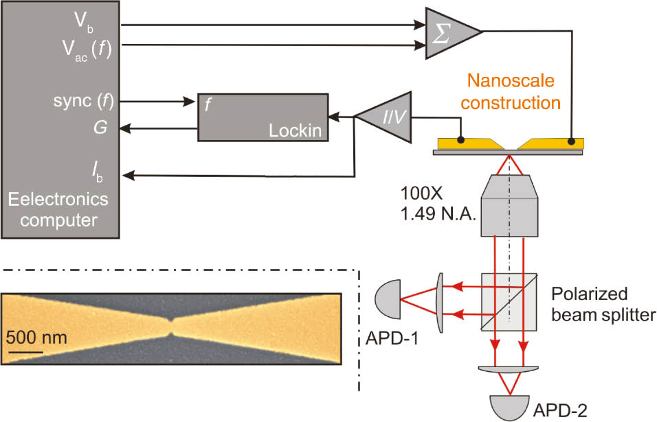
Experimental setup used for measuring simultaneously electron transport and light emission during the electromigration of a Au constriction shown in the inset.
The electromigration is facilitated by controlling the voltage applied to the constriction. The latter is the sum of a d.c. contribution (Vb) and an a.c. one (Vac) oscillating at a frequency f. A current-to-voltage converter (I/V) provides a measure of the current flowing in the constriction (Ib). The conductance (G) of the device is extracted by lock-in detection at f, and the photons are collected by a high-numerical-aperture objective and measured with two cross-polarized avalanche photodiodes (APD-1, APD-2).
2.2 Electrical controls
Electromigration of the constriction is carried out at ambiant conditions. We apply a variable voltage source Vb along with a 20 mV alternative voltage Vac oscillating at frequency f=12.1 kHz. Vac is used to extract the conductance G of the device with lock-in detection (HF2LI Zurich Instrument).
2.3 Optical interrogations
We align the constriction to the focus of an inverted optical microscope (Nikon Eclipse) equipped with a high-numerical-aperture (NA) objective (NA=1.49). We detect the light activity during the electromigration process by capturing the photon emission with two single-photon-counting avalanche photodiodes (APD; SPCM-AQR, Perkin Elmer). The quantum efficiency of the APDs sets the detected spectral range to photon energies spanning the visible and near-infrared region (ca. 1.2–3.1 eV). We use a cross-polarized detection scheme to discriminate photons with an electric field aligned with the main axis of the geometry from those emitted with a transverse polarization state, an expected signature from surface-plasmon-mediated emission of such biased nanoscale contact [29]. All experiments are performed at room temperature in a laboratory environment.
3 Experimental results
3.1 Time traces
Figure 2 shows examples of the time traces recorded at the end of the electromigration process taken before and after the electrical failure of two different devices. Both time traces display the simultaneous dynamics of the normalized conductance (right axis) and the photon counts (left axis). The applied voltage is maintained constant at Vb=800 mV in (A) and Vb=700 mV in (B). The time bin of the acquistion is 10 ms. The step-like evolution of the normalized conductance G/G0 suggests that the devices undergo a change of the transport mechanism from ballistic to tunnel; the abrupt passage takes place at t=27.8 s in Figure 2A and at t=64.2 s in Figure 2B. The plateaus in the normalized conductance are consistent with numerous observations reported in the past [24], [25], [27], [28]. There is evidence of sub-quantum steps, especially in the regime where the conductance explores values between 6G0 and 4G0. These noninteger excursions have already been reported in gold contacts [30], [31]. They are linked to the atomic rearrangement of the contact [32], [33] and can be understood from quantized conductors placed in series [34]. In the time traces displayed in Figure 2, the amplitudes of the voltage applied during the last moment reduce the probability of G to explore the smallest integer numbers N×G0 [35], and the last measured step is at approximately N=4 in both cases. We have observed lower quantum numbers in the past [26], [36], but typically with applied voltage before rupture below 500 mV.
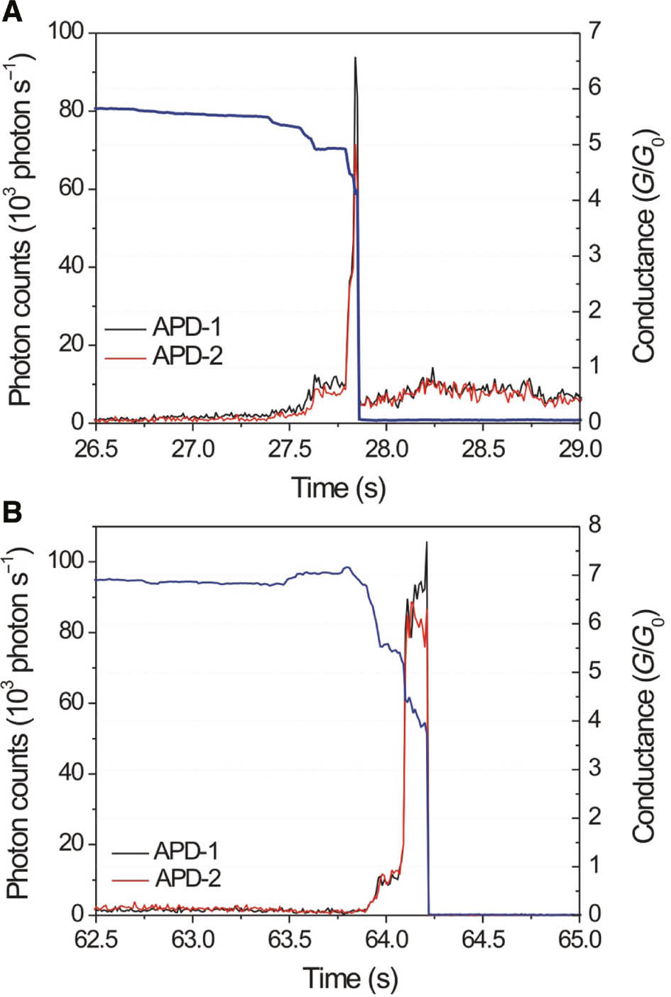
Photon counts and measured conductance versus time.
(A, B) Conductance (normalized) and photon counts time traces captured during the last moment of electromigration for two different devices. The rupture occurs at t=27.8 s in (A) and at t=64.2 s in (B). The conductance is normalized by the quantum of conductance G0. Stepwise closing of conduction channels in approximate units of G0 is correlated with an increase in photon emission. The cross-polarized APD-1 and APD-2 share similar trends.
Figure 2 also displays the simultaneously acquired photon counts measured by the two cross-polarized APDs. In this detected range of counts, the APD counting modules are linear. The graphs show an unambiguous correlation between the conductance steps and light emission. Photons emitted in the detected spectral window are measured as soon as G~5G0, with a rate staying constant for the duration of the conductance plateaus. A tenfold increase of the number of photons is concomitant to the closing of an electron transmission channel identified by the short excursion of G at 4G0 in both examples.
Immediately after the rupture of the device, electron transport occurs by tunneling and the junction features conductances of G=6×10⁻³G0 and G=1.4×10⁻³G0, measured at Vb=800 mV and Vb=700 mV, respectively. In both cases, the photon rate drops when electron transport changes from ballistic to tunnel. Light emission is still observed in this tunneling regime with the junction of Figure 2A.
3.2 Discussion about the mechanisms of light emission
Light emitted by tunnel junctions has been a subject of intense research since Lambe and McCarthy identified the crucial role of inelastic electron coupling to decaying surface plasmons [37]. In the latest advances, tunnel junctions are constituting the active feed of the next generation of electrically driven optical antennas [36], [38], [39], [40]. In this context, engineering the surface plasmon landscape and the barrier height is expected to boost the notoriously low transduction yield plaguing inelastic energy transfer [41], [42], [43]. Continuing on this, a recent proposal suggested that multiple collisions of transported electrons with the boundaries of a plasmonic ballistic constriction may significantly improve the probability to generate an electromagnetic response [29].
During the entire time traces and the excursion of G in the different transport regimes, the photon energy is always greater than the bias energy. The quantum inequality hν≤eVb is systematically violated, where ν is the frequency of the photon. We can thus exclude emission processes akin to inelastic tunneling [44] to explain the light activity. This is further confirmed by the similarity of the signals detected by the two cross-polarized APDs. Inelastic coupling to surface plasmon modes in the metallic contact is expected to show a polarization anistropy [29], [39]. As shown in the time traces of Figure 2, this particular radiative pathway triggered by the decay of surface plasmons is not observed experimentally either in the regime of quantized conduction steps or when the electrons are tunneling. The two cross-polarized signals are at the same count level at all times. Such unpolarized light in the regime of overbias emission confirms our earlier measurement performed with tunnel devices [36], where a wavevector analysis did not show evidence of running surface plasmon. The spatially extended geometrical system introduced by the electrical leads further contributes to the absence of well-defined local surface plasmon resonance.
3.2.1 Tunnel regime: light emission after the rupture
Considering that hν≥eVb, the emission released in the regime of electron tunneling for t≥27.8 s in Figure 2A is due either to the radiative glow of a hot electron distribution [36], [45] or to higher order electron-plasmon interactions [46], [47], [48], [49]. The fast dynamics of the last moment of electromigration prevents us from acquiring information pertaining to the spectral content of the light, which would have been instrumental for discriminating the physical origin of the light emitted in the regime of electron tunneling. For the second device, the smaller applied bias combined with a lower conductance inhibits the emission, if any, to the tail in the detected energy window.
3.2.2 Ballistic regime: light emission before the rupture
The range of conductance values explored here (a few G0) before the tunnel barrier forms is similar to that in the work of Malinowski et al., where infrared emission interpreted as blackbody radiation of an out-of-equilibrium electron gas was measured in mechanically controlled break junctions [45]. Figure 3A is a semilogarithmic plot displaying the dependence of the total photon counts (sum of the two APDs) versus conductance gathered from nine electromigrated devices. The red circles and the light blue diamonds are the experimental points inferred from Figure 2A and B, respectively. The evolution with conductance is consistent across the tested devices: light emission is detected when the conductance of the contact enters 8G0 to 5G0 and dramatically increases up to the breaking point characterized by G<G0. Even in the absence of well-defined quantized steps in the conductance trace, anomalous photon emission from the constriction can be linked to an indirect demonstration of ballistic electron transport in the system.
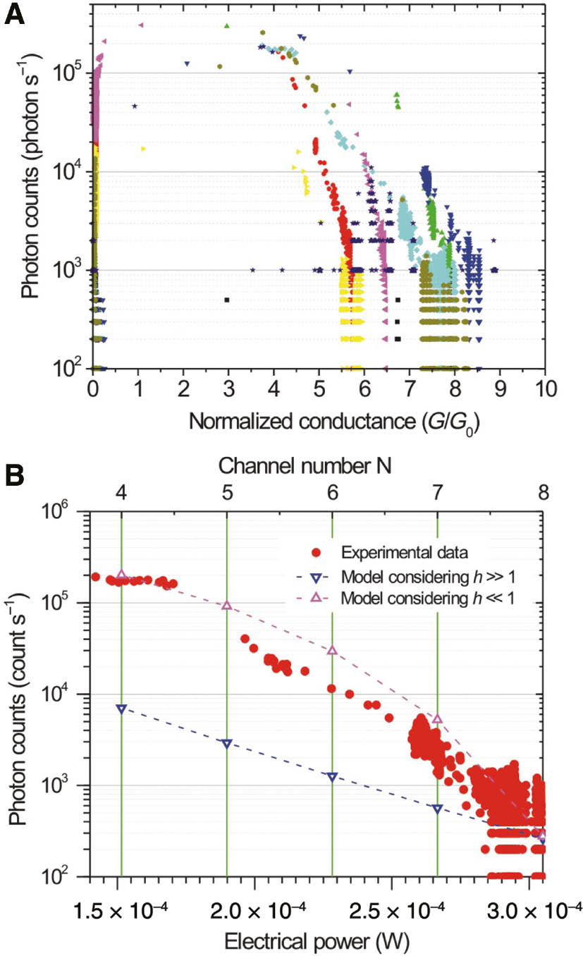
Photo counts versus conductance and electrical power.
(A) Concatenation of results obtained on nine devices showing the evolution of the photon counts (logarithmic scale) with the normalized conductance. The dark count rate of the APDs is about 300 counts s−1. (B) Semilogarithmic plot of the photon count dependence on the dissipated power
The few data points between 4G0 and G0 suggest that the light emission levels off. However, the rapid failure of the contact during the last moment of the electromigration process prevents us from making an affirmative statement. Like the junction displayed in Figure 2A, some devices are optically active in the tunneling regime, as shown by the data points located below G0 in Figure 3A.
Early observations of overbias emission in an atomic contact have shown that it follows a power-law relationship with the electrical power injected in the device. For a given value of the conductance, and regardless of the emission mechanism at play, increasing the current by changing the electrical bias drastically boosts the detected photon counts [45], [46]. In the present experiment, the voltage bias is maintained at a constant value during the last moment of electromigration. The excursion of the conductance in the ballistic regime allows us to monitor the evolution of the photon counts with the electrical power dissipated in the contact without changing the driving conditions and to obtain a deeper insight into the emission mechanism. Light is emitted when the conductance of the contact reaches 5G0, i.e. ~2.5 kΩ. Considering a series resistance of 470 Ω, about 85% of the voltage drop occurs at the constriction. At 4G0, it is 87% of the bias, which is falling. The small difference in the voltage applied cannot account for the one order of magnitude difference of the detected photon counts. Furthermore, the voltage drop is maximum when the contact between the two leads is broken. In this regime of largest potential drop, light emission is either weak or absent in the time traces of Figure 2. For low driving voltages, the process responsible for light emission remains modest and its spectral tail in the visible cannot be discriminated from the background noise. Thus, a trade-off exists between the probability of G to explore few G0 and detecting an overbias light activity. Here, at 700 mV bias, the smallest integer is N=4. When the transport channels are closing, the electrical power dissipated in the contact reduces concomitantly. Figure 3B shows a semilogarithmic plot of the measured light intensity (red circles) versus the electrical power P inferred from Figure 2A before the electrical failure using the relation
4 Analytical model
4.1 Working hypothesis
In the following, we develop a theoretical framework to understand the relationship between the number of channels opened for electron transmission and the optical activity emitted at an overbias photon energy. The delivered electric power scales with the number of transport channels N as
4.2 Model of nonequilibrium electron temperature distribution
Below, we present a qualitative model that illustrates the above consideration. We assume that the electric current is transported by a channel connected to the drain contact through an interconnection region, which we model by a cylinder of radius R0 and finite length Lc, as schematically shown in Figure 4. The electron subsystem in this interconnection region is out of equilibrium because of the fast heating due to the arriving and colliding quasi-ballistic electrons. We assume a local temperature Te for the electrons well above the homogeneous lattice temperature TL. The reader is referred to Ref. [22] for an exhaustive discussion on the temperature of the electronic distribution in driven nonequilibrium nanoscale constrictions. We treat the heat transport problem in this interconnection region in the frame of the two-temperature model, assuming that the lattice temperature TL does not change significantly along the interconnection region.
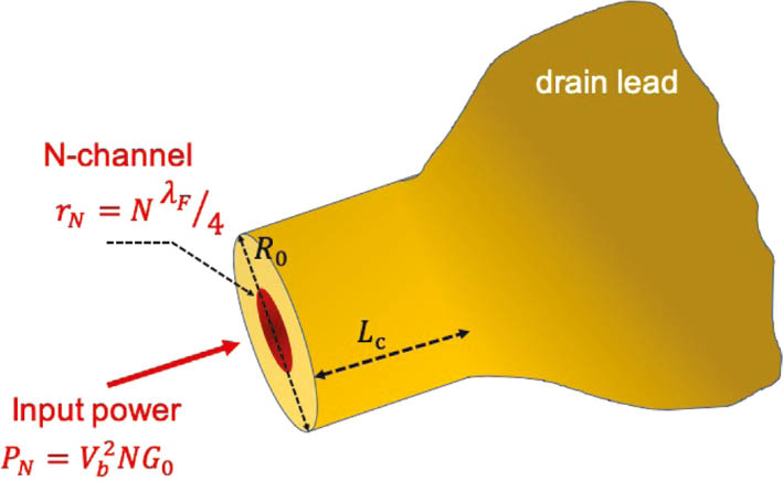
Sketch representing the constriction and the different characteristic parameters used in the model.
4.2.1 Electron temperature
In accordance with the experimental conditions, we will seek a steady-state temperature distribution
where g is the electron-lattice coupling constant, κe is the electron thermal conductivity, and Ce is the electron heat capacity. At electron temperatures below the Fermi temperature Te≤TF, the electron thermal conductivity is given by
With the above estimate, the electron thermal conductivity coefficient scales linearly with the electron temperature: κe≡κe(Te)=b×Te, with the proportionality coefficient
As the natural boundary conditions, we assume the electron temperature in the drain electrode far from the contact to be at the equilibrium with the lattice temperature, so that Te(z=Lc)=TL. At the front end of the contact, z=0 (the z-axis is along the cylinder axis connecting the drain electrode), the electric power is assumed to be homogeneously deposited in a spot with radius rN of opened quantum transport channels N, so that the boundary heat flux is κe(∂Te/∂z)z=0=–pNΘ(r–rN),
At the side wall of the cylinder r=R0, we assume that the heat flux is determined by the energy loss of the electrons in collision with the metal boundary, in analogy with the Fedorovich-Tomchuk mechanism [52]. In this framework, the heat flux at the side wall is proportional to the squared temperature:
Under the above assumptions, the steady-state temperature distribution can be written as
The coefficients an are given by
Here, ζN=rN/R0, μn is the root of the equation μnJ1(μn)/J0(μn)=h with n=0, 1, 2, …, and the eigen values of the problem along the z-axis are
4.2.2 Dependence of Te on the number of transport channels
According to Eq. (2), the maximum temperature is at the center of a hot spot situated at the front end of the cylinder (z=0, r=0). When the side wall heat transfer is fast, i.e. the coefficient h is large (h→+∞), the boundary condition reads Te(r=R0)=TL, and
In the opposite case of vanishing energy exchange at the side wall, i.e. h≪1 or even h=0, the roots
The dependence of the maximum electron temperature versus the number of quantum transport channels is shown in Figure 5A and B for both limiting cases (h≪1 and h≫1) and gradually increasing length Lc of the cylinder interconnection region. The radius of the cylinder is fixed at R0=2.5λF, which corresponds to a maximum of 10 available quantum channels in the contact. For each channel number N, the peak temperature increases with an increase in the cylinder length Lc ranging from Lc=R0/6 to Lc=R0. Obviously, the largest electron temperature is attained when the exchange rate at the side wall is weak (h≪1). We can draw the first important counterintuitive conclusion: regardless of the mechanism dictating the inelastic energy loss at the wall of the constriction, the electronic temperature drops with increasing electrical power dissipation (large N). This dependence is more pronounced for short lengths of the interconnection region when the side wall energy exchange is efficient (h≫1). In the other limiting case (h≪1), a change in the trend appears with increasing Lc, with the occurrence of a maximum shift to higher N. This is the consequence of the first term in brackets in the right-hand side of Eq. (5), which grows linearly with N. In turn, at sufficiently large Lc, the peak temperature will start increasing with N before decreasing. This can be understood from the following argument:
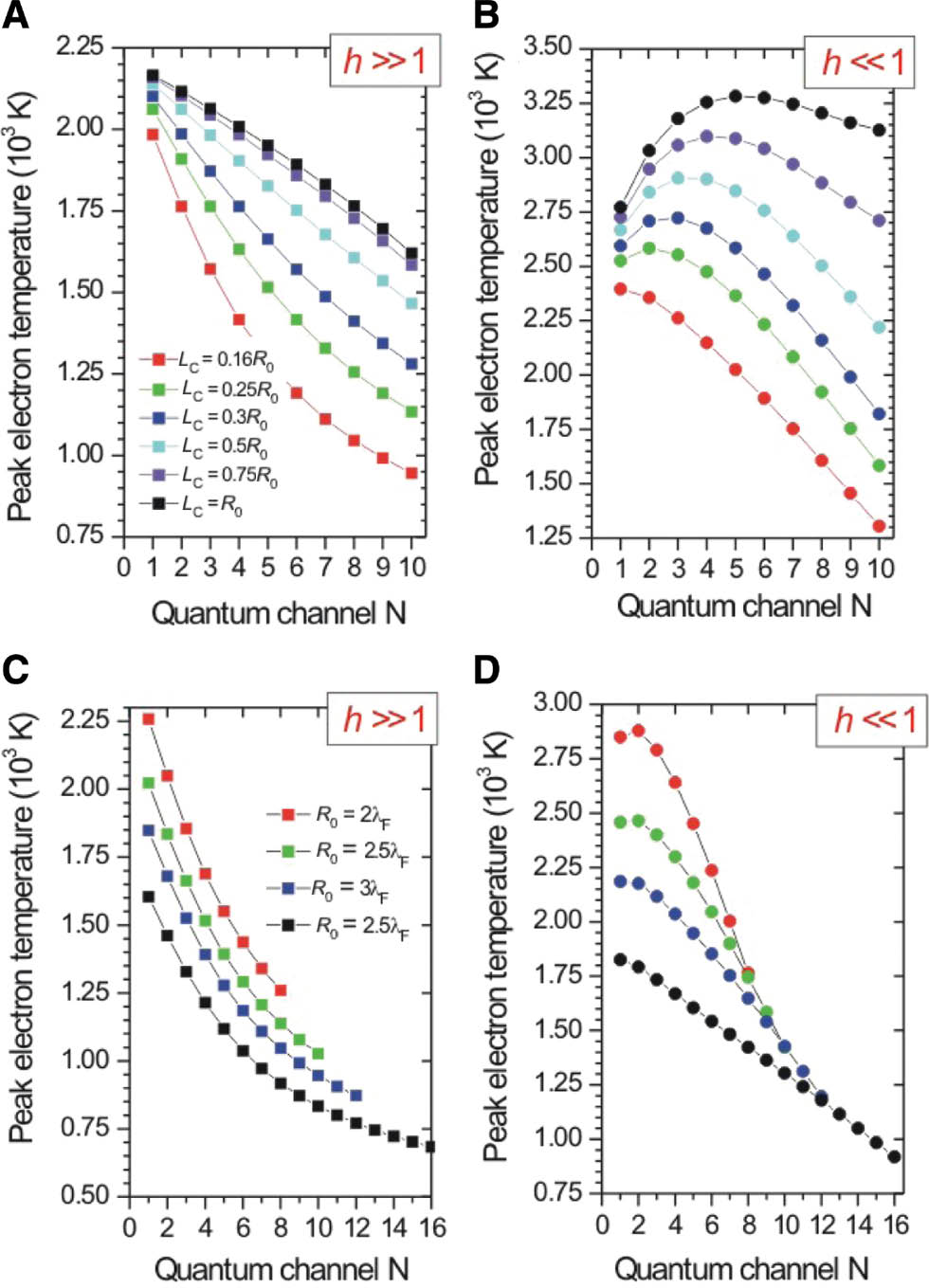
Peak electron temperature versus the number of open quantum channels N in the contact calculated in (A) and (B) at a fixed radius R0=2.5λF, and in (C) and (D) at a fixed cylinder length Lc=λF/2.
Squares represent data at large parameter h≫1, while circles correspond to h≪1. In (A) and (B), data are plotted for different lengths of the interconnection region: Lc=R0/6 (red), Lc=R0/4 (green), Lc=R0/3 (blue), Lc=R0/2 (cyan), Lc=3R0/4 (violet), and Lc=R0 (black). In (C) and (D), the data are plotted for different radii of the cylinder interconnection region: R0=2λF (red), R0=2.5λF (green), R0=3λF (blue), and R0=4λF (black).
In the case of small h, heat is only exchanged at the distal end of the interconnection, and if the length is sufficiently large, all the transverse oscillations exponentially vanish according to Eq. (5) except the constant flow (corresponding to the lowest eigen value), which is proportional to the injected power.
Figure 5C,D displays the dependence of the maximum electron temperature versus the number of quantum transport channels at the fixed length Lc=R0/3 and various radii R0 ranging from R0=2λF (8 quantum channels available) to R0=4λF (16 quantum channels available). The dependences are more pronounced when h≪1 and for smaller radii and become smoother with increase in R0.
Since the electrical power dissipated in the contact areas scales with N (
4.3 Bremsstrahlung emission emerging from nonequilibrium hot electrons colliding with the metal boundary
In a bulk metal, hot nonequilibrium electrons lose their energy mostly during nonradiative collisions with phonons or impurity atoms. Primary photons are emitted as a result of the corresponding Bremsstrahlung processes (at temperatures of our interest, one can omit photons emitted in bound-bound transitions in lattice atoms). Establishment of thermal equilibrium of photons is the consequence of complicated kinetics of free-free electron transitions consisting in emission and absorption Bremsstrahlung processes as well as the Compton effect [53], [54]. In a simplified diffusion approximation, photon emission can be treated through the radiation transfer equation
where Iω is the radiation intensity spectrum, αω is the absorption coefficient at the given frequency, and Bω(Te) is the equilibrium radiation intensity given by Planck’s law. In a bulk metal, when the optical skin depth
In the case of a small interconnection region near the constriction, the region of elevated electron temperature is given by rN≈NλF/4 and is much smaller than the optical skin depth
To find the photon yield in the electron-wall Bremsstrahlung radiation process, we utilize the conventional quantum mechanical calculation technique, which is analogous to that used in the theory of size-dependent conductivity of thin metal films by Trivedi and Ashcroft [57] as well as in the theory of intersubband transitions in semiconductor quantum wells [58], [59]. We consider a metal slab of the thickness L, which is considered to be sufficiently large to provide limiting transition to the continuous spectrum of electron momentum. Let the coordinate axis z be transverse to the slab boundary and
which satisfies the boundary conditions Ψ(z=0)=Ψ(z=L)=0, kz=(π/L)j, j=1, 2, 3…, is the longitudinal wavenumber,
Here,
Here, dρf is the number density of the final states,
Here,
where S⊥ is the square of the wall boundary, and the velocities νi,z=ħki,z/m and
Let ni be the number density of electrons with the longitudinal component of velocity νi,z; the rate of collisions with the left wall of the metal slab is
In the classical limit ħω→0, i.e. when the energy of scattered electron does not change significantly, one can replace
To find the total photon emission rate per unit surface square, we sum Eq. (12) over all the electron states in the slab, assuming the Fermi distribution fF(ε)=1/(1+exp[(ε–εF)/kBTe]).
where
The total Bremsstrahlung photon number spectrum emission rate given by Eqs. (14) and (15) is a complicated function, which we will analyze in detail elsewhere. To our particular purpose here, we will restrict ourselves by the conditions of our experiment, where the maximum attainable temperature is well below the energy of the collected photons, and we have the following relation between the parameters:
One can easily see that under these conditions, the logarithms in braces in Eq. (15) vanish when the argument exceeds u>εF+ħω and u>εF, respectively. At ħω<u<εF, the term in braces is approximately constant and equals ħω/kBTe≫1. At εF<u<εF+ħω, it almost linearly decreases to zero. As a result, we arrive at the following approximation:
Compared to the Planck formula for blackbody radiation
the rate of Bremsstrahlung emission is less by the factor
which under the experimental condition can be estimated to be β~0.1.
To model the total yield of Bremsstrahlung photons detected in our experiment, we integrate the spectrum rate [Eq. (17)] with the transmission function Q(ω) of the detection path, which includes the spectral sensitivity of the detector. The APD response restricts the detection efficiency to overbias photon energy tailing in the visible part of the spectrum. We model the spectral response of the APDs by the following function:
Here, ω1 corresponds to the detection threshold of the detector at a wavelength λ1=1070 nm, ω2 corresponds to the peak of detection efficiency at λ2=740 nm, and ω3 is taken at λ3=600 nm.
One can easily check that for the domain of interest, i.e. for peak temperatures below 3.5×10³ K (see Figure 5), the integrated Bremsstrahlung photon yield is well approximated by the relation dNph/dSdt≈6.13×1022× ζ2exp(–1/ζ)cm−2s−1, where the normalized temperature is ζ=kBTe/ħω1. The results of our calculation of the Bremsstrahlung photon yield rate dependence on the quantum channel number are shown in Figure 6 both for limiting values of the parameter h governing the heat transfer at the side wall of the system and for varying lengths Lc and radii R0 of the interconnection region. The data correspond to the calculated peak temperatures shown in Figure 5. One can find that these dependences at sufficiently small values of length Lc and radius R0 qualitatively recover the experimental data shown in Figure 3A, notably the exponential decay of the photon counts with the number of channels opened. We use the model described above to match the experimental dependence of the photon counts versus electrical power delivered in the contact displayed in Figure 3B, again considering the two extreme heat exchange scenarios at the side wall. The open blue and magenta triangles in Figure 3B are the results of the models considering a short cylinder of length Lc=λF/4 and R0=2λF. We estimate the total radiation area as
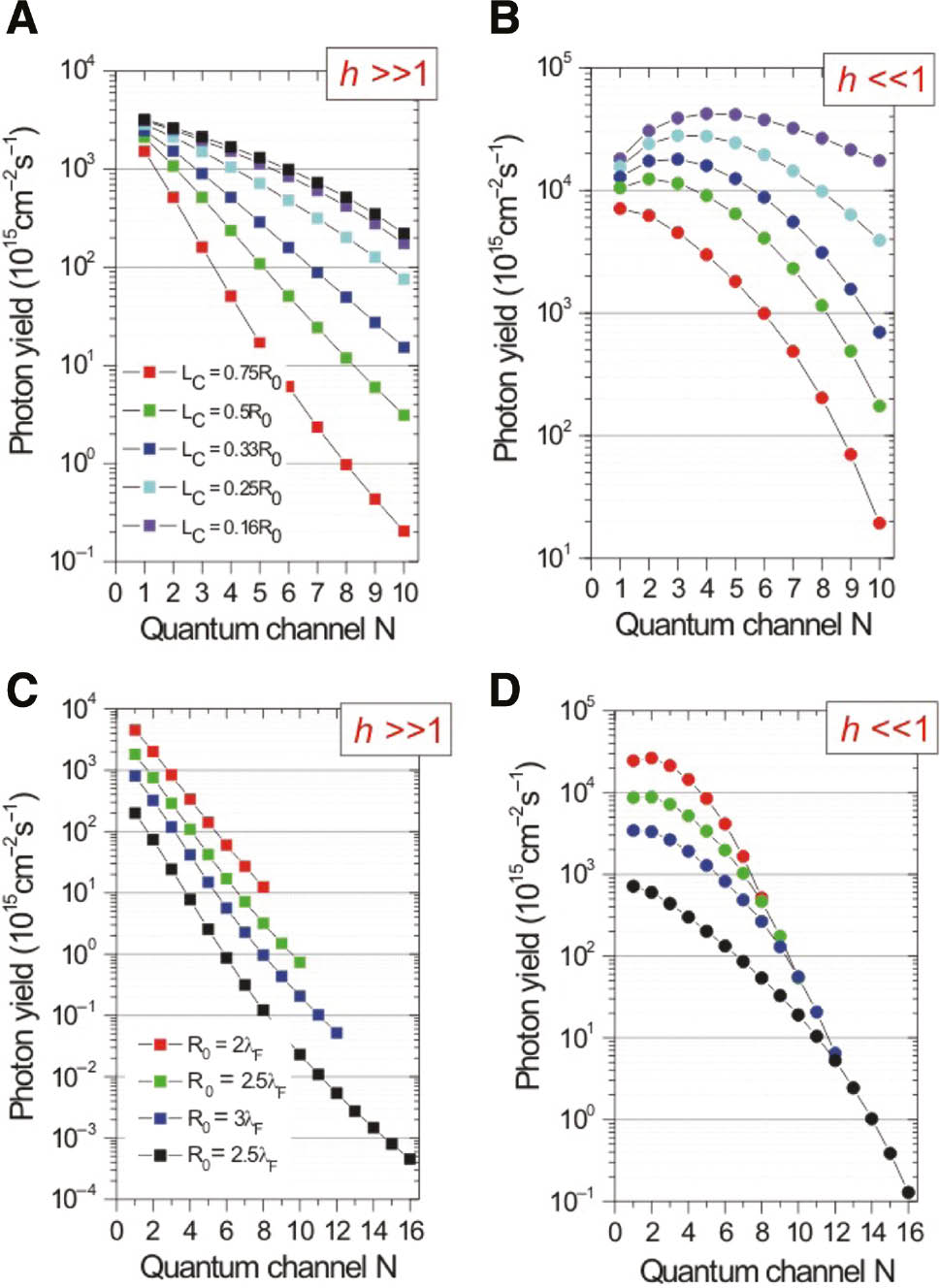
Thermal Bremsstrahlung radiation photon rates versus the number of open quantum channels in the contact.
(A, B) Semilogarithmic plots at a fixed radius R0=2.5λF. Squares represent data at large parameter h≫1 (A), while circles correspond to h≪1 (B). Data are plotted at different lengths of the interconnection region: Lc=R0/6 (red), Lc=R0/4 (green), Lc=R0/3 (blue), Lc=R0/2 (cyan), and Lc=3R0/4 (violet). (C, D) Semilogarithmic plots at fixed cylinder length Lc=λF/2. Data are plotted at different radii of the cylinder interconnection region: R0=2λF (red), R0=2.5λF (green), R0=3λF (blue), and R0=4λF (black).
5 Conclusions
Past research in atomic-size point contacts has provided a firm understanding of the radio frequency electromagnetic response occurring when the system is driven in the linear regime of low bias voltages (e.g. in the mV range). Recent reports have suggested that electrons transported through the contact with a large kinetic energy (~eV) may unveil new nonlinear mechanisms of light emission. Our findings show that photons with energies much higher than the kinetic energy of the electron are emitted during the formation of the contact when the transport becomes ballistic. Our experiment has revealed that the number of photons collected exponentially increases when the quantized transport channels are closing. By assuming an electron distribution near the contact, which is no longer at equilibrium with the phonon population, we derived a model relating the electron temperature and the photon yield to the number of channels. We find that the out-of-equilibrium electron temperature distribution increases when quantum channels are closing during the electromigration process. Within this model, we assumed the presence of a small interconnection region between the quantum channel and the body of the drain contact, in which transport of hot electrons proceeds in a quasi-ballistic manner. Energy exchange in this interconnection region is mainly guided by electron collisions at the side wall rather than electron-phonon and electron-electron interactions. Hot electrons emit photons in an overbias spectral domain as a result of the Bremsstrahlung process driven by the boundary of the interconnection region. We derived (to our knowledge, for the first time) the quantum mechanical formula for the rate of this Bremsstrahlung photon emission, which in the limit ħω→0 coincides with the classical relation. We found qualitative agreement between the estimated emission rates and the results of our measurements. At that stage of the research, the dynamics leading to the formation of the contact remains too rapid to interrogate the spectrum of the emitted photons and their statistics. Once we have a reliable strategy to control the closing and opening of the electron transport channels, these findings will contribute to the development and engineering of integrated, electrically driven optical light sources at atomic length scales.
Funding source: European Research Council
Award Identifier / Grant number: 306772
Funding source: European Cooperation in Science and Technology
Award Identifier / Grant number: RFBR-17-58-150007
Funding source: Russian Science Foundation
Award Identifier / Grant number: 17-19-01532
Funding statement: This work was funded by the European Research Council under the European Community’s Seventh Framework program FP7/2007-2013 Grant Agreement 306772, Funder Id: http://dx.doi.org/10.13039/100011199, the CNRS/RFBR collaborative research program number 1493, Funder Id: http://dx.doi.org/10.13039/501100000921 (Grant RFBR-17-58-150007), the COST Action MP1403 “Nanoscale Quantum Optics” supported by COST (European Cooperation in Science and Technology), and the Regional Excellence funding scheme (project APEX). A.U. and I.S are thankful to the Russian Science Foundation (Grant 17-19-01532, Funder Id: http://dx.doi.org/10.13039/501100006769) for additional support. Access to the nanofabrication facility ARCEN Carnot was financed by the Regional council of Burgundy and la Délégation Régionale à la Recherche et à la Technologie (DRRT).
References
[1] Agraït N, Yeyati AL, van Ruitenbeek JM. Quantum properties of atomic-sized conductors. Phys Rep 2003;377:81–279.10.1016/S0370-1573(02)00633-6Suche in Google Scholar
[2] Cui L, Jeong W, Hur S, et al. Quantized thermal transport in single-atom junctions. Science 2017;355:1192–5.10.1126/science.aam6622Suche in Google Scholar PubMed
[3] Datta S. Electronic transport in mesoscopic systems. Cambridge studies in semiconductor physics and microelectronic engineering. Cambridge, Cambridge University Press, 1995.Suche in Google Scholar
[4] van Houten H, Beenaker C. Quantum point contacts. Phys Today 1996;49:22.10.1063/1.881503Suche in Google Scholar
[5] Green F, Das MP. Noise and transport in mesoscopics: physics beyond the landauer-büttiker formalism. Fluct Noise Lett 2005;5:C1–14.10.1142/S0219477505002355Suche in Google Scholar
[6] Das MP, Green F. Mesoscopic transport revisited. J Phys Condens Matter 2009;21:101001.10.1088/0953-8984/21/10/101001Suche in Google Scholar PubMed
[7] Todorov TN. Local heating in ballistic atomic-scale contacts. Philos Mag B 1998;77:965–73.10.1080/13642819808206398Suche in Google Scholar
[8] Agraït N, Untiedt C, Rubio-Bollinger G, Vieira S. Onset of energy dissipation in ballistic atomic wires. Phys Rev Lett 2002;88:216803.10.1103/PhysRevLett.88.216803Suche in Google Scholar PubMed
[9] Frederiksen T, Brandbyge M, Lorente N, Jauho A-P. Inelastic scattering and local heating in atomic gold wires. Phys Rev Lett 2004;93:256601.10.1103/PhysRevLett.93.256601Suche in Google Scholar PubMed
[10] Reznikov M, Heiblum M, Shtrikman H, Mahalu D. Temporal correlation of electrons: suppression of shot noise in a ballistic quantum point contact. Phys Rev Lett 1995;75:3340–3.10.1103/PhysRevLett.75.3340Suche in Google Scholar PubMed
[11] Kumar M, Avriller R, Yeyati AL, van Ruitenbeek JM. Detection of vibration-mode scattering in electronic shot noise. Phys Rev Lett 2012;108:146602.10.1103/PhysRevLett.108.146602Suche in Google Scholar PubMed
[12] Beenakker CJ, Schomerus H. Antibunched photons emitted by a quantum point contact out of equilibrium. Phys Rev Lett 2004;93:096801.10.1103/PhysRevLett.93.096801Suche in Google Scholar
[13] Lebedev AV, Lesovik GB, Blatter G. Statistics of radiation emitted from a quantum point contact. Phys Rev B 2010;81:155421.10.1103/PhysRevB.81.155421Suche in Google Scholar
[14] Fulga IC, Hassler F, Beenakker CWJ. Nonzero temperature effects on antibunched photons emitted by a quantum point contact out of equilibrium. Phys Rev B 2010;81:115331.10.1103/PhysRevB.81.115331Suche in Google Scholar
[15] Zakka-Bajjani E, Dufouleur J, Coulombel N, Roche P, Glattli DC, Portier F. Experimental determination of the statistics of photons emitted by a tunnel junction. Phys Rev Lett 2010;104:206802.10.1103/PhysRevLett.104.206802Suche in Google Scholar
[16] Forgues J-C, Gasse G, Lupien C, Reulet B. Non-classical radiation emission by a coherent conductor. C R Phys 2016;17:718–28. [Quantum microwaves/Micro-ondes quantiques.]10.1016/j.crhy.2016.07.004Suche in Google Scholar
[17] Rogovin R, Scalapino DJ. Fluctuation phenomena in tunnel junctions. Ann Phys 1974;86:1–90.10.1016/0003-4916(74)90430-8Suche in Google Scholar
[18] Février P, Gabelli J. Tunneling time probed by quantum shot noise. Nat Commun 2018;9:4940.10.1038/s41467-018-07369-6Suche in Google Scholar
[19] Fedorovich R, Naumovets A, Tomchuk P. Electron and light emission from island metal films and generation of hot elctrons in nanoparticles. Phys Rep 2000;328:73–9.10.1016/S0370-1573(99)00094-0Suche in Google Scholar
[20] Green F, Thakur JS, Das MP. Where is the shot noise of a quantum point contact? Phys Rev Lett 2004;92:156804.10.1103/PhysRevLett.92.156804Suche in Google Scholar PubMed
[21] D’Agosta R, Sai N, Di Ventra M. Local electron heating in nanoscale conductors. Nano Lett 2006;6:2935–8.10.1021/nl062316wSuche in Google Scholar PubMed
[22] Chen R, Wheeler PJ, Ventra MD, Natelson D. Enhanced noise at high bias in atomic-scale Au break junctions. Sci Rep 2014;4:4221.10.1038/srep04221Suche in Google Scholar PubMed PubMed Central
[23] Park H, Lim AKL, Park J, Alivisato AP, McEuen PL. Fabrication of metallic electrodes with nanometer separation by electromigration. Appl Phys Lett 1999;75:301.10.1063/1.124354Suche in Google Scholar
[24] Umeno A, Hirakawa K. Nonthermal origin of electromigration at gold nanojunctions in the ballistic regime. Appl Phys Lett 2009;94:162103.10.1063/1.3124654Suche in Google Scholar
[25] Trouwborst ML, van der Molen SJ, van Wees BJ. The role of joule heating in the formation of nanogaps by electromigration. J Appl Phys 2006;99:114316.10.1063/1.2203410Suche in Google Scholar
[26] Dasgupta A, Buret M, Cazier N, et al. Electromigrated electrical optical antennas for transducing electrons and photons at the nanoscale. Beilstein J Nanotechnol 2018;9:1964–76.10.3762/bjnano.9.187Suche in Google Scholar PubMed PubMed Central
[27] Strachan D, Smith D, Johnston D, et al. Controlled fabrication of nanogaps in ambient environment for molecular electronics. Appl Phys Lett 2005;86:043109.10.1063/1.1857095Suche in Google Scholar
[28] Hoffmann R, Weissenberger D, Hawecker J, Stöffler D. Conductance of gold nanojunctions thinned by electromigration. Appl Phys Lett 2008;93:043118.10.1063/1.2965121Suche in Google Scholar
[29] Uskov AV, Khurgin JB, Buret M, Bouhelier A, Smetanin IV, Protsenko IE. Biased nanoscale contact as active element for electrically driven plasmonic nanoantenna. ACS Photon 2017;4:1501–5.10.1021/acsphotonics.7b00272Suche in Google Scholar
[30] O’Neill K, Osorio EA, van der Zant HSJ. Self-breaking in planar few-atom au constrictions for nanometer-spaced electrodes. Appl Phys Lett 2007;90:133109.10.1063/1.2716989Suche in Google Scholar
[31] Mangin A, Anthore A, Della Rocca ML, Boulat E, Lafarge P. Reduced work functions in gold electromigrated nanogaps. Phys Rev B 2009;80:235432.10.1103/PhysRevB.80.235432Suche in Google Scholar
[32] Muller CJ, van Ruitenbeek JM, de Jongh LJ. Conductance and supercurrent discontinuities in atomic-scale metallic constrictions of variable width. Phys Rev Lett 1992;69:140–3.10.1103/PhysRevLett.69.140Suche in Google Scholar PubMed
[33] Kizuka T, Kodama S, Matsuda T. Verification of unzipping models of electromigration in gold nanocontacts by in situ high-resolution transmission electron microscopy. Nanotechnology 2010;21:495706.10.1088/0957-4484/21/49/495706Suche in Google Scholar PubMed
[34] de Heer W, Frank S, Ugarte D. Fractional quantum conductance in gold nanowires. Z Phy B Condens Matter 1997;104:469–73.10.1007/s002570050477Suche in Google Scholar
[35] Fujii A, Ichi Mizobata J, Kurokawa S, Sakai A. Stability of atom-sized metal contacts under high biases. e-J Surf Sci Nanotechnol 2004;2:125–30.10.1380/ejssnt.2004.125Suche in Google Scholar
[36] Buret M, Uskov AV, Dellinger J, et al. Spontaneous hot-electron light emission from electron-fed optical antennas. Nano Lett 2015;15:5811–8.10.1021/acs.nanolett.5b01861Suche in Google Scholar PubMed
[37] Lambe J, McCarthy SL. Light emission from inelastic electron tunneling. Phys Rev Lett 1976;37:923–5.10.1103/PhysRevLett.37.923Suche in Google Scholar
[38] Kern J, Kullock R, Prangsma JC, Emmerling M, Kamp M, Hecht B. Electrically-driven optical antennas. Nat Photon 2015;9:582–6.10.1038/nphoton.2015.141Suche in Google Scholar
[39] Parzefall M, Bharadwaj P, Jain A, Taniguchi T, Watanabe K, Novotny L. Antenna-coupled photon emission from hexagonal boron nitride tunnel junctions. Nat Nanotechnol 2015;10:1058.10.1038/nnano.2015.203Suche in Google Scholar PubMed
[40] Qian H, Hsu S-W, Gurunatha K, et al. Efficient light generation from enhanced inelasticelectron tunnelling. Nat Photon 2018;12:485–8.10.1038/s41566-018-0216-2Suche in Google Scholar
[41] Bigourdan F, Hugonin J-P, Marquier F, Sauvan C, Greffet J-J. Nanoantenna for electrical generation of surface plasmon polaritons. Phys Rev Lett 2016;116:106803.10.1103/PhysRevLett.116.106803Suche in Google Scholar PubMed
[42] Uskov AV, Khurgin JB, Protsenko II, Smetanin IV, Bouhelier A. Excitation of plasmonic nanoantennas by nonresonant and resonant electron tunnelling. Nanoscale 2016;8: 14573–9.10.1039/C6NR01931ESuche in Google Scholar
[43] Parzefall M, Szabó Á, Taniguchi T, Watanabe K, Luisier M, Novotny L. Light from van der waals quantum tunneling devices. Nat Commun 2019;10:292.10.1038/s41467-018-08266-8Suche in Google Scholar
[44] Parzefall M, Bharadwaj P, Novotny L. Quantum plasmonics. In: Bozhevolnyi SI, Martin-Moreno L, Garcia-Vidal F, eds. Springer series in solid-state sciences, Vol. 185. Berlin Heidelberg, Germany, Springer, 2017:211–36.10.1007/978-3-319-45820-5_10Suche in Google Scholar
[45] Malinowski T, Klein HR, Iazykov M, Dumas P. Infrared light emission from nano hot electron gas created in atomic point contacts. Europhys Lett 2016;114:57002.10.1209/0295-5075/114/57002Suche in Google Scholar
[46] Schull G, Néel N, Johansson P, Berndt R. Electron-plasmon and electron-electron interactions at a single atom contact. Phys Rev Lett 2009;102:057401.10.1103/PhysRevLett.102.057401Suche in Google Scholar
[47] Xu F, Holmqvist C, Belzig W. Ovembias light emission due to high-order quantum noise in a tunnel junction. Phys Rev Lett 2014;113:066801.10.1103/PhysRevLett.113.066801Suche in Google Scholar
[48] Kaasbjerg K, Nitzan A. Theory of light emission from quantum noise in plasmonic contacts: above-threshold emission from higher-order electron-plasmon scattering. Phys Rev Lett 2015;114:126803.10.1103/PhysRevLett.114.126803Suche in Google Scholar
[49] Peters P-J, Xu F, Kaasbjerg K, Rastelli G, Belzig W, Berndt R. Quantum coherent multielectron processes in an atomic scale contact. Phys Rev Lett 2017;119:066803.10.1103/PhysRevLett.119.066803Suche in Google Scholar
[50] Ashcroft NW, Mermin ND. Solid state physics, 3rd ed. Philadelphia, PA, Saunders College, 1968.Suche in Google Scholar
[51] Kanavin AP, Smetanin IV, Isakov VA, et al. Heat transport in metals irradiated by ultrashort laser pulses. Phys Rev B 1998;57:14698–703.10.1117/12.376993Suche in Google Scholar
[52] Belotskii ED, Tomchuk PM. Electron-phonon interaction and hot electrons in small metal islands. Surf Sci 1990;239:143–55.10.1016/0039-6028(90)90626-JSuche in Google Scholar
[53] Kompaneets A. The establishment of thermal equilibrium between quanta and electrons. Sov Phys JETP 1957;4: 730–7.Suche in Google Scholar
[54] Zeldovich YB. Interaction of free electrons with electromagnetic radiation. Sov Phys Usp 1975;18:79–98.10.1070/PU1975v018n02ABEH001947Suche in Google Scholar
[55] Chopra KL, Bobb LC, Francombe MH. Electrical resistivity of thin single crystal gold films. J Appl Phys 1963;34:1699–702.10.1063/1.1702662Suche in Google Scholar
[56] Ghisellini G. Radiative processes in high energy astrophysics. Lecture notes in physics. Heidelberg, Springer, 2013.10.1007/978-3-319-00612-3Suche in Google Scholar
[57] Trivedi N, Ashcroft NW. Quantum size effects in transport properties of metallic films. Phys Rev B 1988;38:12298–309.10.1103/PhysRevB.38.12298Suche in Google Scholar PubMed
[58] Smet J, Fonstad C, Hu Q. Intrawell and interwell intersubband transitions in multiple quantum wells for far infrared sources. J Appl Phys 1996;79:9305.10.1063/1.362607Suche in Google Scholar
[59] Nag B. Physics of quantum well devices. New York, Kluwer Academic Publishers, 2002.Suche in Google Scholar
[60] Landau L, Lifshitz E. The classical theory of fields, Vol. 2. Oxford, Pergamon Press, 1971.Suche in Google Scholar
©2020 Alexandre Bouhelier et al., published by De Gruyter, Berlin/Boston
This work is licensed under the Creative Commons Attribution 4.0 Public License.
Artikel in diesem Heft
- Editorial
- Proceedings of the 9th International Conference on Surface Plasmon Photonics (SPP9)
- Research Articles
- Ground state chemistry under vibrational strong coupling: dependence of thermodynamic parameters on the Rabi splitting energy
- Ultrastrong coupling in single plexcitonic nanocubes
- Strong coupling between organic dye molecules and lattice modes of a dielectric nanoparticle array
- Ultrastrong coupling effects in molecular cavity QED
- Circular dichroism mode splitting and bounds to its enhancement with cavity-plasmon-polaritons
- Quantum theory of surface-enhanced resonant Raman scattering (SERRS) of molecules in strongly coupled plasmon–exciton systems
- Probing graphene’s nonlocality with singular metasurfaces
- Ultra-compact integrated graphene plasmonic photodetector with bandwidth above 110 GHz
- GeSe nanosheets modified surface plasmon resonance sensors for enhancing sensitivity
- Exciton-plasmon polariton coupling and hot carrier generation in two-dimensional SiB semiconductors: a first-principles study
- Second harmonic imaging of plasmonic Pancharatnam-Berry phase metasurfaces coupled to monolayers of WS2
- Near-IR wide-field-of-view Huygens metalens for outdoor imaging applications
- Focused vortex-beam generation using gap-surface plasmon metasurfaces
- Effective medium concept in temporal metamaterials
- Helium focused ion beam direct milling of plasmonic heptamer-arranged nanohole arrays
- Strongly coupled, high-quality plasmonic dimer antennas fabricated using a sketch-and-peel technique
- Effect of quantized conductivity on the anomalous photon emission radiated from atomic-size point contacts
- Tunneling-induced broadband and tunable optical emission from plasmonic nanorod metamaterials
- Review
- Terahertz quantum plasmonics at nanoscales and angstrom scales
- Research Articles
- Fundamental limits of hot carrier injection from metal in nanoplasmonics
- Nanoantennas with balanced gain and loss
- Review
- Perspective: plasmon antennas for nanoscale chiral chemistry
- Research Articles
- Plasmonic nanofocusing spectral interferometry
- Mono-crystalline gold platelets: a high-quality platform for surface plasmon polaritons
- Tailoring the plasmonic Fano resonance in metallic photonic crystals
- Darkfield colors from multi-periodic arrays of gap plasmon resonators