
Tunable atom-trapping based on a plasmonic chiral metamaterial
-
Zhao Chen

 ,
Sai Chen
,
Sai Chen

Abstract
Chiral metamaterials provide a very convenient way to actively regulate the light field via external means, which is very important in nanophotonics. However, the very weak chiral response of a generally planar metamaterial severely limits its application. Therefore, it is important to design a system with large circular dichroism. Here we report an optical metamaterial with strong chirality in a bilayer gear-shaped plasmonic structure and consider this chiral response of such fields on tunable atom (87Rb) trapping. Simulation results show that maximum chiral response is observed when the two layers of the gear-shaped structures are rotated from each other by an angle of 60° at λ = 760 nm. Also, we demonstrate an active tunable potential for three-dimensional stable atom-trapping with tunable range of position and potential of a neutral atom of ~58 nm and ~1.3N mK (N denotes the input power with unit mW), respectively. In addition, the trap centers are about hundreds of nanometers away from the structure surface, which ensures the stability of the trapping system. The regulation of neutral atom trapping broadens the application of chiral metamaterials and has potential significance in the manipulation of cold atoms.
1 Introduction
The configuration of metamaterials which can be designed and manipulated to obtain extraordinary properties has attracted considerable attention in recent years [1], [2]. A wide variety of functional devices can be realized in such systems [3], including but not limited to sensors [4], [5], polarizers [6], [7], [8], and photodetectors [9], [10], [11], [12]. Among them, there is a class of metamaterials with a special structure, named chiral metamaterials, which shows different electromagnetic response, also called chirality, to right- and left-handed circularly polarized (RCP and LCP) light [13], [14], [15]. This unique optical response renders chiral metamaterials highly promising candidates for a variety of applications [16], [17], [18], [19], [20], [21], [22], [23], [24], [25], [26], [27], [28], [29], [30]. In general, chiral metamaterials are designed to be single-layered (planar chiral metamaterial) because of the relative ease of their fabrication [16], [17], [18], [19], [20], [21]. However, the chiral responses are very weak and typically require oblique incidence. In order to obtain a large chiral response in the case of normal incidence, various novel chiral structures have been designed [31], [32], [33], [34]. For instance, Cui et al. demonstrated a giant chiral optical response from a twisted-arc metamaterial [31]. Chen et al. realized strong optical chirality based on slanted plasmonic nanoapertures [32]. Rodrigus et al. proposed a double-layered ellipse hole to achieve intensity-dependent modulation [33]. Rajaei et al. experimentally reported giant circular dichroism (CD) with ramp-shaped plasmonic nanostructures [34]. In the above-mentioned works [16], [17], [18], [19], [20], [21], [22], [23], [24], [25], [26], [27], [28], [29], [30], [31], [32], [33], [34], we find that all designs are based on structure-surface-confined field effects to realize a variety of applications while ignoring spatial effects such as neutral atom trapping, an application that requires a noncontact field to be implemented.
As is known, optically trapped atoms, e.g. 87Rb, 133Cs, have been used for precision metrology and quantum information processing because a neutral atom is an excellent frequency reference and atoms trapped in an optical field have long coherence times and long lifetimes [35]. At present, a common method of trapping neutral atoms is by using optical dipole traps [36]. This kind of trapping uses the potential well generated by the incident field to push/pull the atom into the potential dip and is independent of the particular sublevel state of the trapped atoms. Much of the work on atom trapping has been achieved using optical nanofibers [37], [38], [39], [40], [41], [42]. However, the optical nanofiber cannot enhance the light field and requires a large input power, which will reduce the life of the trapped atoms. On the other hand, in order to increase the stability of the trapping system, the surface potential must be overcome, which increases the complexity of the system and difficulty of the experiment [37], [38], [39], [40], [41], [42]. To address this problem, neutral atom trapping based on surface plasmon (SP) was proposed [43], [44], and later a plasmonic nanohole-array-based stable 3D atom trapping was also achieved [45]. Nevertheless, creating tunable optical traps compatible with optical nanostructures is still a challenge, so it is essential to make such trapping tunable via external means at the nanoscale.
In this article, we report a novel type of chiral metamaterial for atom-trapping based on plasmonic, bilayered, gear-shaped nanoapertures, with the layers rotated from each other by an angle of 60° in silver films. The basic design principle is to obtain the largest transmitted power difference between RCP and LCP at the blue detuned trap wavelength for 87Rb. Simulation results show that the maximum differential transmittance is observed at λ=760 nm. Also, an active tunable potential for 3D stable optical trapping at the nanoscale is demonstrated. By changing the phase of the circularly polarized light (RCP to LCP or LCP to RCP), the tunable range of position and potential of the trapped atoms is about ~58 nm and 1.3N mK because of the different near-field scattering intensities. Our structure is very compact and easy to fabricate by the focused ion beam milling process. Combining neutral atom trapping with chiral metamaterial plasmonic structures would open the possibility of achieving ultracompact functional optical components in highly integrated optics.
2 Designed chiral plasmonic structure
The schematic diagram of our setup is illustrated in Figure 1A. The unit cell of the novel chiral plasmonic structure consists of two thin silver layers (h=90 nm) each of which has been perforated in the shape of a gear, and which are rotated from each other by an angle α=60°. The point O in Figure 1A denotes the origin of coordinate, and the direction of the arrow is positive. The second film layer is grown on a silica (refractive index nsilica=1.45) substrate and is separated from the first layer by a thin silica layer of d=350 nm. The silica layers are continuous without any hole in their structure, and the silica does not fill the chiral opening at the bottom metal. Figure 1B shows the top view of the first and second silver films. The proposed structure can be made by plasma-enhanced chemical vapor deposition (PECVD) and focused-ion-beam (FIB) writing. The relative permittivity of silver is taken from the literature [46] and expanded using the method of interpolation by 1 nm. The module Wave Optics (Electromagnetic Waves, Frequency Domain) in COMSOL Multiphysics 5.2a is used to investigate the optical response of the proposed structure. Here, the periodic boundary conditions are set to the x- and y-direction of the unit cell, and perfectly matched layer absorbing conditions are set on the top (with Port 2 “off”)/bottom (with Port 1 “on”) sides. Then, the S-parameters of abs(ewfd.S21)2, which can be extracted from the model, express the transmission spectrum of the system. The CP light port modes are set as the electric mode field: Ex=exp(–j×k0×nsilica×z), Ey=exp(–j×k0×nsilica×z+ja), and Ez=0 (k0=2π/λ denotes free-space wave vector, a ϵ (0, 2π) represents the phase of CP light, and a=π/2 or 3π/2 corresponds to LCP or RCP, respectively). The other optimized parameters are set as follows: P=700 nm, L=300 nm, and w=150 nm. The purpose of optimizing the parameters is to obtain the maximum chiral response at the trapping wavelength so as to adjust the position and potential energy of the trapped atoms to the maximum extent. The calculated transmission spectra for RCP (black curve) and LCP (red curve) incidences are shown in Figure 2A. It is clearly observed that a pronounced plasmonic resonance is present at λ=760 nm under RCP incidence, whereas the transmission under LCP incidence is strongly suppressed, leading to a large differential transmittance. In order to distinguish it from circular dichroism (CD), a typical feature of a chiral response, which is defined as the difference in absorption of RCP and LCP [13], [14], [15], we named the differential transmittance as CD_T, which is shown in Figure 2B. The maximum value in Figure 2B means that the difference in electric intensities between RCP and LCP is the largest, which provides a basis for subsequent adjustment of potential and position for trapped neutral atoms. Figure 2C,D displays the electric field intensity distributions (the positions of the first and second layer correspond to the plane z=0 and z=–440 nm for one unit cell, respectively.) under RCP and LCP illumination at the resonant wavelength λ=760 nm. The distributions of the hot spots related to the enhancement of the electric field show a clear dependence on the polarization of the incident light, resulting in a large difference in transmittance of RCP and LCP light. Beyond that, the circular state of polarization is perfectly preserved in the transmitted wave, with a conversion ratio less than 0.16% between RCP and LCP, shown as the inset in Figure 2A. The appearance of the CD_T spectrum can be attributed to the broken mirror symmetry due to the index mismatch between the superstrate and the substrate [47].
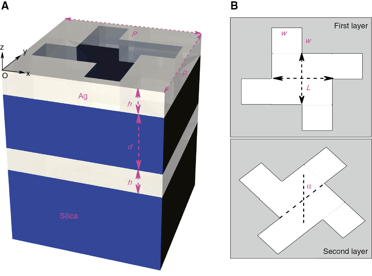
Schematic of chiral metamaterial.
(A) A single unit cell of the gear-shaped metamaterial array and the geometrical parameter symbols. (B) The top view of the silver film: the two layers of the gear-shaped structure are rotated from each other by an angle α=60°.
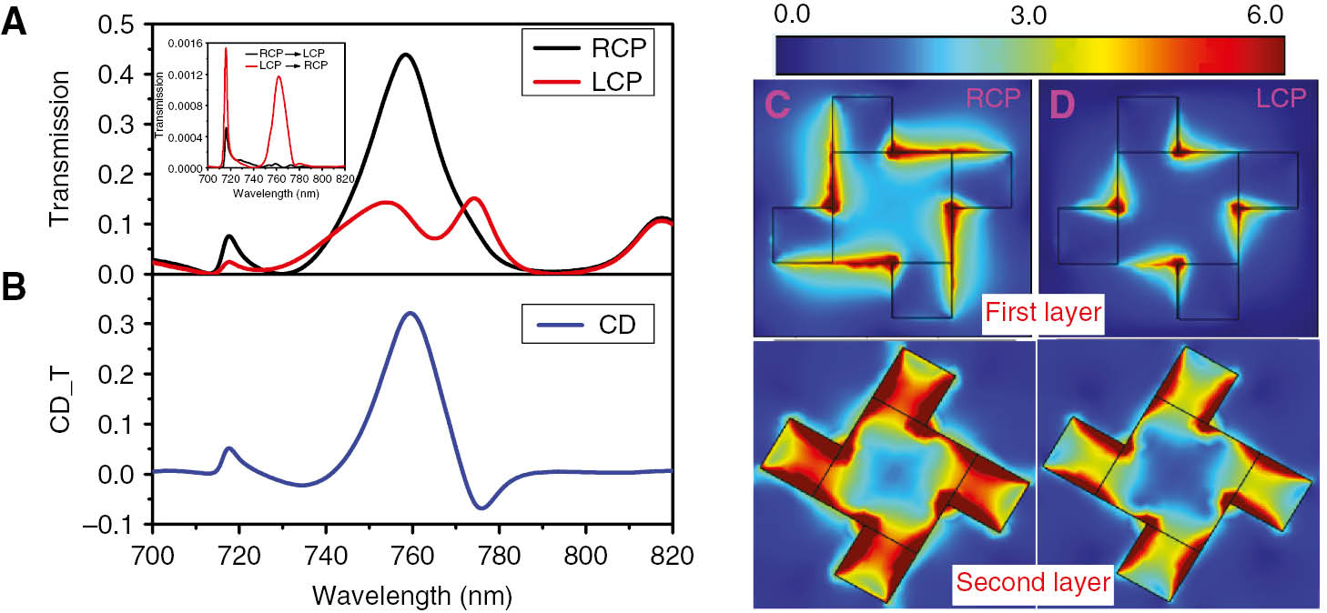
The circular dichroism of the structure.
(A) Simulation results of the normalized zero-order transmission spectrum for RCP (black curve) and LCP (red curve) incidences. (B) The CD_T spectrum corresponding to (A). Electric field intensity maps under (C) RCP and (D) LCP excitations at λ=760 nm. Inset: simulated circular-polarization-conversion spectra.
3 Analysis of atom-trapping for 87Rb
According to previous literature [44], [45], [48], we know that the near-field scattering effect of the periodic plasmonic structure can produce a local electric field minimum in the spatial extent of the system. In our system, RCP and LCP light incidence cause different scattering intensities, which in turn make the local electric field minimum adjustable. Here, we consider this phenomenon in neutral atom (87Rb) trapping. To better understand the advantages of the system in terms of atom-trapping, we plot the spatial electric field intensity (|E|2) distributions of the proposed structure at λ=760 nm at x=0 or y=0 plane for one unit cell, which are shown in Figure 3A,B for RCP and LCP excitations, respectively. (It is to be noted that the electric field distributions are the same at x=0 or y=0 plane only when LCP or LCP light excites because of the peculiarity of the structure.) The resonant wavelength λ=760 nm is selected to be blue-detuned to the D2 line of 87Rb atoms [45], [48]. By the way, the proposed trapping platform is suitable for trapping neutral atoms with all the transition wavelengths greater than 760 nm, e.g. 133Cs. Apparently, a trap center (local electric field minimum) emerges at each plot, which is about hundreds of nanometers away from the structure surface. Here, ds (ds=379 nm for LCP and ds=321 nm for RCP) denotes the distance between the structure surface (z=0) and the trap center. A neutral atom, i.e. 87Rb atom, can be trapped in the trap center via optical dipole forces with blue-detuned light [36].
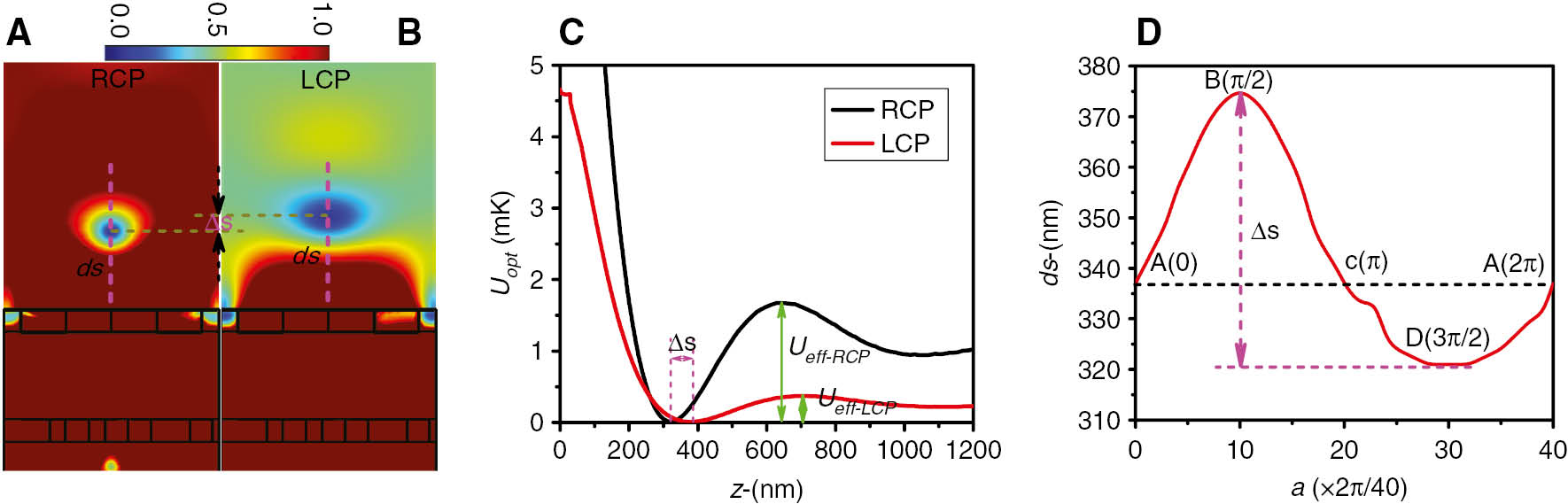
Quantitative description for the trapping ability of the system.
Normalized spatial electric field intensity (|E|2) distributions for (A) RCP and (B) LCP excitations at x=0 or y=0 plane. (C) Corresponding optical dipole potential Uopt distributions along the pink dashed lines in A and B with input power P0=1 mW. (D) The variation law of ds with change in a.
As is known, a neutral atom in an electric field will be affected by two kinds of potentials [36]. One is the optical dipole potential, Uopt, which can be expressed as
In order to further analyze the 3D trapping property of the system, we plot the distributions of Uopt in the x-y plane at the trapping wavelength λ=760 nm, as shown in Figure 4A. Figure 4B shows the corresponding optical dipole potential (Uopt) distributions for RCP (black line) and LCP (red line) through the x or y centering direction. It can be easily seen that the trap depths are about 1.1 mK and 0.42 mK for RCP and LCP incidences, respectively, with input power P0=1 mW. The full width at the half-maxima (FWHMs) are both about 225 nm for RCP and LCP, which can be used to confine and trap a single atom [49]. Manipulation of a single atom can be used to verify basic physical laws and for accurate measurements of physical constants. Figure 4C shows the trap centers of periodic arrays at z=ds in the x-y plane. (Here, we use 4×4 unit cells to represent an infinitely extended array. However, due to limitations of computer memory and because the Comsol Multiphysics software mesh cannot be evenly divided, the trap centers show a small asymmetry.) The periodic structure guarantees the uniformity of trap depths in each unit cell, which greatly reduces the detection error due to the variance of cooling efficiency and the photon scattering rate from each atom [38], [39], [40], [41], [42], [45], [48]. In addition, atom array trapping can be used to realize resonance fluorescence. Through the above analysis, a tunable, stable 3D atom array trapping independent of the surface potential based on a plasmonic chiral metamaterial is demonstrated. The ability to regulate neutral atoms at the subwavelength scale would enable quantum network capabilities and large-scale quantum communications. In addition, our systems can also enable refractive index sensors, as well as circular polarization detectors, which are very important in nanophotonics.
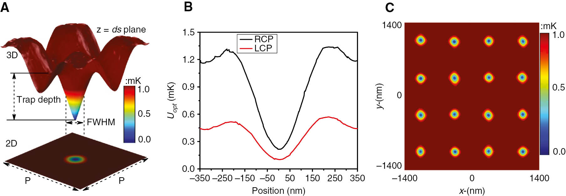
3D trapping property of the system.
(A) Distributions of Uopt of the z=ds plane in 2D and 3D at the trapping wavelength λ=760 nm for one unit cell. (B) Corresponding optical dipole potential Uopt distributions for RCP (black line) and LCP (red line) through x/y centering direction. (C) Periodic arrays at z=ds in the x-y plane.
4 Conclusion
In conclusion, we have demonstrated tunable and stable 3D atom array trapping based on the large circular dichroism in a plasmonic chiral metamaterial made up of a double-layer gear-shaped structure. Simulation results showed that under RCP excitation, there is a transmission resonance peak at λ=760 nm, while the transmission is almost completely suppressed by LCP excitation. Because of the near-field scattering, a trap center, about hundreds of nanometers (321 nm for RCP and 379 nm for LCP) away from the structure surface, emerges, which guarantees the stability of the trapped atoms. Different electric field intensities make the trapped atoms tunable by altering the phase of the CP light. The proposed structure can be easily fabricated and integrated on a chip. This type of atom-trapping method, based on the regulation of LCP and RCP light, holds promise for atomic on-chip integration, which will have great significance in quantum information processing and nanophotonics.
Funding source: National Natural Science Foundation of China (NSFC)
Award Identifier / Grant number: 11704013
Funding statement: This work was supported by the National Natural Science Foundation of China (NSFC) (11704013), Funder Id: http://dx.doi.org/10.13039/501100001809 and the National Science and Technology Innovation Special Zone Program of China.
References
[1] Engheta N, Ziolkowski RW, editors. Metamaterials: physics and engineering explorations. John Wiley & Sons, 2006.10.1002/0471784192Suche in Google Scholar
[2] Cui TJ, Smith DR, Liu R. Metamaterials. New York, NY, Springer, 2010.10.1007/978-1-4419-0573-4Suche in Google Scholar
[3] Tong XC. Functional metamaterials and metadevices. Bolingbrook, IL, Springer, 2018.10.1007/978-3-319-66044-8Suche in Google Scholar
[4] He Y, Lawrence K, Lngram W, Zhao Y. Circular dichroism based refractive index sensing using chiral metamaterials. Chem Commun 2016;52:2047–50.10.1039/C5CC07742GSuche in Google Scholar
[5] Wang W, Yan F, Tan S, Zhou H, Hou Y. Ultrasensitive terahertz metamaterial sensor based on vertical split ring resonators. Photon Res 2017;5:571–7.10.1364/PRJ.5.000571Suche in Google Scholar
[6] Zhao Y, Alu A. Manipulating light polarization with ultrathin plasmonic metasurfaces. Phys Rev B 2011;84:205428.10.1103/PhysRevB.84.205428Suche in Google Scholar
[7] Zhao Y, Belkin M, Alu A. Twisted optical metamaterials for planarized ultrathin broadband circular polarizers. Nat Commun 2012;3:870.10.1038/ncomms1877Suche in Google Scholar PubMed
[8] Ji R, Wang S, Liu X, Chen X, Li W. Broadband circular polarizers constructed using helix-like chiral metamaterials. Nanoscale 2016;8:14725–9.10.1039/C6NR01738JSuche in Google Scholar PubMed
[9] Song S, Ma X, Pu M, et al. Tailoring active color rendering and multiband photodetection in a vanadium-dioxide-based metamaterial absorber. Photon Res 2018;6:492–7.10.1364/PRJ.6.000492Suche in Google Scholar
[10] Venuthurumilli PK, Ye PD, Xu X. Plasmonic resonance enhanced polarization sensitive photodetection by black phosphorus in near infrared. ACS Nano 2018;12:4861–7.10.1021/acsnano.8b01660Suche in Google Scholar PubMed
[11] Bai Q. Manifestation of the spontaneous parity-time symmetry breaking phase transition in hot-electron photodetection based on a tri-layered metamaterial. Nanophotonics 2019;8:495–504.10.1515/nanoph-2018-0207Suche in Google Scholar
[12] Lee H, Lee H, Park JY. Direct imaging of surface plasmon-driven hot electron flux on the Au nanoprism/TiO2. Nano Lett 2019;19:891–6.10.1021/acs.nanolett.8b04119Suche in Google Scholar PubMed
[13] Schäferling M. Chiral nanophotonics. Cham, Switzerland, Springer International Publishing, 2017.10.1007/978-3-319-42264-0Suche in Google Scholar
[14] Qu Y, Huang L, Wan L, Zhang Z. Giant circular dichroism induced by tunable resonance in twisted Z-shaped nanostructure. Opt Express 2017;15:5480–7.10.1364/OE.25.005480Suche in Google Scholar PubMed
[15] Wang Z, Wang Y, Adamo G, Teng J, Sun H. Induced optical chirality and circularly polarized emission from achiral CdSe/ZnS quantum dots via resonantly coupling with plasmonic chiral metasurfaces. Laser Photon Rev 2019;13:1800276.10.1002/lpor.201800276Suche in Google Scholar
[16] Klimov VV, Zabkov IV, Pavlov AA, Shiu RC, Chan HC, Guo GY. Manipulation of polarization and spatial properties of light beams with chiral metafilms. Opt Express 2016;24:6172–85.10.1364/OE.24.006172Suche in Google Scholar PubMed
[17] Ye W, Yuan X, Guo C, Zhang J, Yang B, Zhang S. Large chiroptical effects in planar chiral metamaterials. Phys Rev App 2017;7:054003.10.1103/PhysRevApplied.7.054003Suche in Google Scholar
[18] Feng X, Bai Y, Jing Z, et al. Enhanced circular dichroism of tilted zigzag-shaped nanohole arrays. Appl Opt 2019;58: 177–81.10.1364/AO.58.000177Suche in Google Scholar PubMed
[19] Dyakov SA, Semenenko VA, Gippius NA, Tikhodeev SG. Magnetic field free circularly polarized thermal emission from a chiral metasurface. Phys Rev B 2018;98:235416.10.1103/PhysRevB.98.235416Suche in Google Scholar
[20] Qi J, Zhang M, Zhang Y, et al. Multiband circular dichroism from bilayer rotational F4 nanostructure arrays. Appl Opt 2019;58:479–84.10.1364/AO.58.000479Suche in Google Scholar PubMed
[21] Bai Y, Wang T, Ullah H, Qu Y, Abudukelimu A, Zhang Z. Asymmetric transmission in the planar chiral nanostructure induced by electric and magnetic resonance at the same wavelength. Annalen der Physik 2019;531:1800469.10.1002/andp.201800469Suche in Google Scholar
[22] Sakllari I, Yin X, Nesterov ML, Terzaki K, Xomalis A, Farsari M. 3D chiral plasmonic metamaterials fabricated by direct laser writing: the twisted omega particle. Adv Opt Mater 2017;5:1700200.10.1002/adom.201700200Suche in Google Scholar
[23] Pan M, Li Q, Hong Y, Cai L, Lu J, Qiu M. Circular-polarization-sensitive absorption in refractory metamaterials composed of molybdenum zigzag arrays. Opt Express 2018;26:17772–80.10.1364/OE.26.017772Suche in Google Scholar PubMed
[24] Liang S, Zhang W, Yuan J, et al. In-plane gap plasmon induced strong circular dichroism in double-layer Archimedean planar metamaterials. Opt Mater Express 2018;8:2870–9.10.1364/OME.8.002870Suche in Google Scholar
[25] Wu Z, Chen X, Wang M, Dong J, Zheng Y. High-performance ultrathin active chiral metamaterials. ACS Nano 2018;12: 5030–41.10.1021/acsnano.8b02566Suche in Google Scholar PubMed
[26] Wang Z, Ai B, Zhou Z, Guan Y, Mohwald H, Zhang G. Free-standing plasmonic chiral metamaterials with 3D resonance cavities. ACS Nano 2018;12:10914–23.10.1021/acsnano.8b04106Suche in Google Scholar PubMed
[27] Chen Y, Gao J, Yang X. Direction-controlled bifunctional metasurface polarizers. Laser Photon Rev 2018;12:1800198.10.1002/lpor.201800198Suche in Google Scholar
[28] Yang S, Liu Z, Hu S, et al. Spin-selective transmission in chiral folded metasurfaces. Nano Lett 2019. DOI: 10.1021/acs.nanolett.8b04521.Suche in Google Scholar PubMed
[29] Klos G, Miola M, Sutherland DS. Increased refractive index sensitivity by circular dichroism sensing through reduced substrate effect. J Phys Chem C 2019;123:7347–55.10.1021/acs.jpcc.8b12152Suche in Google Scholar
[30] Cao T, Mao L, Qiu Y, et al. Fano resonance in asymmetric plasmonic nanostructure: separation of sub-10 nm enantiomers. Adv Opt Mater 2019;7:1801172.10.1002/adom.201801172Suche in Google Scholar
[31] Cui Y, Kang L, Lan S, Rodriues S, Cai W. Giant chiral optical response from a twisted-arc metamaterial. Nano Lett 2014;14:1021–5.10.1021/nl404572uSuche in Google Scholar PubMed
[32] Chen Y, Gao J, Yang X. Chiral metamaterials of plasmonic slanted nanoapertures with symmetry breaking. Nano Lett 2018;18:520–7.10.1021/acs.nanolett.7b04515Suche in Google Scholar PubMed
[33] Rodrigus SP, Lan S, Kang L, et al. Intensity-dependent modulation of optically active signals in a chiral metamaterial. Nat Commun 2017;8:10462.10.1038/ncomms14602Suche in Google Scholar PubMed PubMed Central
[34] Rajaei M, Zeng J, Albooyeh M, et al. Giant circular dichroism at visible frequencies enabled by plasmonic pamp-shaped nanostructures. ACS Photon 2019;6:924–31.10.1021/acsphotonics.8b01584Suche in Google Scholar
[35] Lee J, Park DH, Mittal S, Dagenais M, Rolston SL. Integrated optical dipole trap for cold neutral atoms with an optical waveguide coupler. New J Phys 2013;15:043010.10.1088/1367-2630/15/4/043010Suche in Google Scholar
[36] Grimm R, Weidemuller M. Optical dipole traps for neutral atoms. Adv At Mol Opt Phys 2000;42:1–39.10.1016/S1049-250X(08)60186-XSuche in Google Scholar
[37] Nieddu T, Gokhroo V, Chormaic SN. Optical nanofibers and neutral atoms. J Opt 2016;18:053001.10.1088/2040-8978/18/5/053001Suche in Google Scholar
[38] Qi X, Baragiola BQ, Jessen PS, Deutsch IH. Dispersive response of atoms trapped near the surface of an optical nanofiber with applications to quantum nondemolition measurement and spin squeezing. Phys Rev A 2016;93:023817.10.1103/PhysRevA.93.023817Suche in Google Scholar
[39] Goban A, Choi KS, Alton DJ, et al. Demonstration of a state-insensitive, compensated nanofiber trap. Phys Rev Lett 2012;109:033603.10.1103/PhysRevLett.109.033603Suche in Google Scholar PubMed
[40] Vetsch E, Reitz D, Sague G, Schmidt R, Dawkins ST, Rauschenbeutel A. Optical interface created by laser-cooled atoms trapped in the evanescent field surrounding an optical nanofiber. Phys Rev Lett 2010;104:203603.10.1103/PhysRevLett.104.203603Suche in Google Scholar PubMed
[41] Balykin VI, Hakuta K, Le Kien F, Liang JQ, Morinaga M. Atom trapping and guiding with a subwavelength-diameter optical fiber. Phys Rev A 2004;70:011401(R).10.1103/PhysRevA.70.011401Suche in Google Scholar
[42] Le Kien F, Balykin VI, Hakuta K. Atom trap and waveguide using a two-color evanescent light field around a subwavelength-diameter optical fiber. Phys Rev A 2004;70:063403.10.1103/PhysRevA.70.063403Suche in Google Scholar
[43] Chang DE, Thompsin JD, Park H, et al. Trapping and manipulation of isolated atoms using nanoscale plasmonic structures. Phys Rev Lett 2009;103:123004.10.1103/PhysRevLett.103.123004Suche in Google Scholar PubMed
[44] Gullans M, Tiecke T, Chang DE, et al. Nanoplasmonic lattices for ultracold atoms. Phys Rev Lett 2012;109:235309.10.1103/PhysRevLett.109.235309Suche in Google Scholar PubMed
[45] Chen Z, Zhang F, Zhang Q, et al. Blue-detuned optical atom trapping in a compact plasmonic structure. Photon Res 2017;5:436–40.10.1364/PRJ.5.000436Suche in Google Scholar
[46] Johson PB, Christy RW. Optical constants of the noble metals. Phys Rev B 1972;6:4370–9.10.1103/PhysRevB.6.4370Suche in Google Scholar
[47] Kuwata-Gonokami M, Saito N, Ino Y, et al. Giant optical activity in quasi-two-dimensional planar nanostructures. Phys Rev Lett 2005;95:227401.10.1103/PhysRevLett.95.227401Suche in Google Scholar PubMed
[48] Chen Z, Zhang F, Duan X, Zhang T, Gong Q, Gu Y. Chiral-plasmon-tuned potentials for atom trapping at the nanoscale. Adv Opt Mater 2018;6:1800261.10.1002/adom.201800261Suche in Google Scholar
[49] Zhang PF, Li G, Zhang TC. Subwavelength optical dipole trap for neutral atoms using a microcapillary tube tip. J Phys B: At Mol Opt Phys 2017;50:045005.10.1088/1361-6455/aa5518Suche in Google Scholar
[50] Chang DE, Sinha K, Taylor JM, Kimble HJ. Trapping atoms using nanoscale quantum vacuum forces. Nat Commun 2014;5:4343.10.1038/ncomms5343Suche in Google Scholar PubMed PubMed Central
Supplementary Material
The online version of this article offers supplementary material (https://doi.org/10.1515/nanoph-2019-0163).
© 2019 Zhao Chen, Lin Xiao et al., published by De Gruyter, Berlin/Boston
This work is licensed under the Creative Commons Attribution 4.0 Public License.
Artikel in diesem Heft
- Review Articles
- Optically accessible memristive devices
- Role of nanophotonics in the birth of seismic megastructures
- Perovskite nanocrystals for energy conversion and storage
- Coherent nonlinear optics of quantum emitters in nanophotonic waveguides
- Optical force microscopy: combining light with atomic force microscopy for nanomaterial identification
- Enhanced nanodrug delivery in tumors after near-infrared photoimmunotherapy
- Metal-induced energy transfer
- Progresses in the practical metasurface for holography and lens
- Research Articles
- In-situ electrospun aligned and maize-like AgNPs/PVA@Ag nanofibers for surface-enhanced Raman scattering on arbitrary surface
- Plasmonic near-field scanning nanoscope with a cross-polarization detection technique
- Tunable atom-trapping based on a plasmonic chiral metamaterial
- Rigorous coupled-wave analysis of absorption enhancement in vertically illuminated silicon photodiodes with photon-trapping hole arrays
- Expanded Jones complex space model to describe arbitrary higher-order spatial states in fiber
- Color generation from self-organized metalo-dielectric nanopillar arrays
- Tandem white organic light-emitting diodes stacked with two symmetrical emitting units simultaneously achieving superior efficiency/CRI/color stability
- Ag nanoparticle-enhanced alkyl radical generation in photopolymerization for holographic recording
- Gate-tunable metafilm absorber based on indium silicon oxide
- High-performance and compact broadband terahertz plasmonic waveguide intersection
- Plasmonic quantum effects on single-emitter strong coupling
- Strong coupling with directional absorption features of Ag@Au hollow nanoshell/J-aggregate heterostructures
- Letter
- Broad band infrared modulation using spintronic-plasmonic metasurfaces
- Large-area pixelated metasurface beam deflector on a 12-inch glass wafer for random point generation