Nanocrystalline PbS thin film produced by alkaline chemical bath deposition: effect of inhibitor levels and temperature on the physicochemical properties
-
Veli Şimşek

 and
Mustafa Oğuzhan Çağlayan
and
Mustafa Oğuzhan Çağlayan

Abstract
In this study, nanocrystalline PbS film coating on a glass slide was done using the chemical bath deposition method. PbS film was deposited in an alkaline solution using Pb(NO3)2, CS(NH2)2, and the inhibitor (Na2S2O3) for 30–120 min at room temperature (25 °C) and 40 °C, and inhibitor levels were investigated in the range of 3.2 mM–12.7 mM. The physicochemical properties of the obtained thin films were investigated by scanning electron microscopy, MAPPING, atomic force microscopy, fourier-transform infrared spectroscopy, water contact angle and X-ray diffraction analyses. The relationship between nanocrystallite size, distribution, pin-hole development, and synthesis conditions were examined using image processing and surface response methodology. The band gap of the produced PbS thin film was calculated using FT-IR analysis results (0.41 eV).
1 Introduction
Thin films are now widely used in the fabrication of semiconductor instruments, magnetic recording systems, detection systems, optical coatings, decorative works [1, 2], and spintronic devices [3]. Furthermore, polycrystalline lead (II) sulfide (PbS) thin films have attracted the attention of researchers due to their electrical and photoelectrical properties. Among the semiconductor thin films, polycrystalline lead (II) sulfide (PbS) has attracted great attention from researchers owing to its electrical and photoelectrical properties [4]. It has also been used for various purposes, such as solar control coatings [4], [5], [6], laser diodes [5, 6], catalysts [4], humidity and temperature sensors [4], [5], [6], and solar energy [5, 7]. PbS has both a cubic crystal structure and a direct band gap, and generally shows p-type conductivity. Its band gap is 0.4 eV at 27 °C [8, 9]. This band gap, which belongs to poly-nanocrystalline PbS, corresponds to the near-mid infrared (NIR/MIR, IR-B/C) radiation of approximately 3 µm, and therefore, PbS is used in NIR and MIR detectors [10], [11], [12], [13].
Thin films of PbS can be produced by various methods, including molecular beam deposition [14], spray pyrolysis [15, 16], laser ablation [17], non-vacuum film deposition [18], chemical bath deposition (CBD) [19], vacuum evaporation/co-evoparation [20], thermal evaporation [21], and electrochemical deposition [22]. Today, CBD is widely used to produce both amorphous and crystalline structures [23], due to its low cost and ability to produce high-quality films [11]. Moreover, the CBD method does not require the use of toxic gases and can be used to produce large quantities of thin films in industrial fields [24].
The CBD method has been used for the production of nanocrystalline PbS thin films. These studies gave contributions to the development of the CBD method for PbS film deposition. The molar ratio of the reactants for this method has been studied by several researchers [25, 26]. In addition, the synthesis temperature, which is an important parameter that affects the uniformity of the produced PbS, has been investigated in a wide range of temperatures from room temperature (RT) to 80 °C [27–34]. Moreover, there is also a study evaluating the inhibitory effect of PbS production under alkaline conditions [35]. However, there is no study that deals with the effect of temperature change on film formation together with the inhibitor effect. In addition, good conditions have not yet been determined for PbS produced by the CBD method.
This study was aimed at investigating the effect of inhibitor concentration together with the effect of temperature (at RT, 25 °C and 40 °C) on the physicochemical properties of PbS films produced in alkaline conditions. The effect of temperature, concentration, reaction time, and speed on the nanocrystalline structure is great in the CBD method. Which parameters are effective in the method applied in this study were evaluated using surface response methodology (SRM). This evaluation was carried out on the grain size and distribution determined by image processing in electron microscopy results. The physical properties of the produced PbS films were determined by X-ray diffraction (XRD), fourier-transform infrared spectroscopy (FT-IR), water contact angle (WCA), atomic force microscopy (AFM), scanning electron microscopy (SEM), MAPPING, and ultraviolet and visible (UV–vis) analyses.
2 Experimental
All chemicals were purchased from the local distributor of Sigma-Aldrich and Merck companies. Analytical grade chemicals were used without further purification. Solutions were prepared using de-ionized water. Otherwise stated, all experiments were done in duplicate.
2.1 Synthesis of PbS thin films
The CBD method was applied by modification of procedures previously applied for the synthesis of PbS [35]. The chemical precipitation reactions of PbS can be expressed as follows: [36].
Within the scope of the study, PbS films were synthesized with the CBD method in 100 mL of deionized water, at 25 °C, 40 °C, and at different concentrations of Na2S2O3 (0.00316 M, 0.00632 M, 0.00948 M, and 0.01265 M) for 30, 60, 90, and 120 min. Tables 1 and 2 show the chemical data used in the synthesis of PbS thin films.
Chemicals, amounts and time used in the synthesis of PbS thin films at RT (100 mL solution).
| Experiment | Pb(NO3)2 (g) | NaOH (g) | CS(NH2)2 (g) | Na2S2O3 (g) | Time (min) |
|---|---|---|---|---|---|
| A | 0.295 | 0.584 | 0.388 | 0.050 | 30 |
| B | 0.295 | 0.584 | 0.388 | 0.100 | 60 |
| C | 0.295 | 0.584 | 0.388 | 0.150 | 90 |
| D | 0.295 | 0.584 | 0.388 | 0.200 | 120 |
Chemicals, amounts and time used in the synthesis of PbS thin films at the 40 °C temperature (100 mL solution).
| Experiment | Pb(NO3)2 (g) | NaOH (g) | CS(NH2)2 (g) | Na2S2O3 (g) | Time (min) |
|---|---|---|---|---|---|
| A | 0.295 | 0.584 | 0.388 | 0.050 | 30 |
| B | 0.295 | 0.584 | 0.388 | 0.100 | 60 |
| C | 0.295 | 0.584 | 0.388 | 0.150 | 90 |
| D | 0.295 | 0.584 | 0.388 | 0.200 | 120 |
Synthesis steps:
The bath bowl was first filled with the Pb(NO3)2 aqueous solution. After that, NaOH aqueous solution was added. The solution turned a white, milky color with the addition of NaOH. Pb(OH)2 ions in the solution are thought to be responsible for the milk color. The solution turns clear within 2–3 min. Then, Na2S2O3 was added before CS(NH2)2 was added to the aqueous solution. Finally, CS(NH2)2 was added to the solution. Synthesis of PbS thin films was carried out at different times according to the molar concentration of Na2S2O3 (Tables 1 and 2).
2.2 Characterization studies
To determine the phase structures of synthesized PbS thin films, the Panalytical Empryan HT-XRD instrument was used. All patterns of PbS thin films were investigated using XRD at 40 kV (high voltage tension) and 30 mA (current) using Cu-Kα (= 0.154 nm) radiation with a 0.066 step size and over a 5°–90° range. FT-IR analyses of PbS thin films were carried out using a Perkin Elmer IR instrument in the range of 4000–400 cm−1. The surface morphology and surface roughness properties of PbS (RT and 40 °C) thin films were investigated with an Ambios Q-Scope AFM. AFM analyses were performed under room conditions with an NSC16 console, the resonance frequency of 185.8 kHz, console force constant of 42 N m−1, non-contact mode, and AFM Q-Scope automatic operating software mode. Moreover, to determine the elemental composition and surface morphological structure of PbS thin films, SEM and MAPPING analyses were carried out using the Zeiss SUPRA V 40 instrument.
3 Results and discussion
3.1 Characterization studies
Figure 1 shows XRD patterns of synthesized PbS thin films at RT (Figure 1a), 40 °C (Figure 1b), and different Na2S2O3 concentrations (0.00316 M, 0.00632 M, 0.00948 M, and 0.01265 M) for 30, 60, 90, and 120 min. The cubic shaped grain structure of PbS thin films was identified by the diffraction patterns in the high angle range between 2θ = 20° and 90° with seven peaks which correspond to (d111), (d200), (d220), (d311) [37], (d222), (d400), and (d331) of ordered cubic structures. All PbS thin films had a clear (d111 and 200) [38, 39]. The main Bragg peaks for PbS are located at 2θ = 25.94°, 30.04°, 43.16°, 50.98°, 53.50°, 61.64°, 64.68°, and 68.77°. The crystallite sizes corresponding to different conditions were calculated with the Scherrer Equation as follows:

XRD patterns of nanoscale PbS thin films: (a) RT, (b) 40 °C.
In the above expression of the Scherrer Equation, “D” (the average size of the crystallites), “k” (the particle shape factor, k = 0.91 for PbS), “λ” (the X-ray wavelengt = λ = 0.1542 nm), “β (radian)” and “θB” are the full width at half-maximum (FWHM) intensity and the Bragg angle, respectively. To determine the PbS nanoparticle crystalline size, the values associated with the (d111), (d200), (d220), and PbS plane in the Scherrer Equation were used. Although UV analyses of PbS thin films were performed, the analyses could not be used because, PbS is detected in the infared region and not in the ultraviolet spectrum region. In this study, band gaps of PbS thin films were calculated using FT-IR analysis results working in the infrared region. Band gaps of samples were obtained by using the absorption peak of PbS at between 2980 and 3030 cm−1 (Figure 2a and b small images). The direct band gap of bulk PbS thin films is 0.41 eV at 27 °C [8, 9]. Using the FT-IR analysis results of PbS thin films obtained at RT and 40 °C, the band gap values of the PbS thin films were calculated as 0.41 eV (Tables 3 and 4). Moreover, the crystallite sizes pertaining to the PbS thin films obtained at diverse conditions (Table 3). It is clear that an increased intensity and peak number were directly in relation to increasing time and amount of Na2S2O3 (Figure 1a).

FT-IR spectra of PbS (A, B) thin films: (a) RT, (b) 40 °C.
Physical properties of PbS thin films (25 °C).
| Materials | Peak position 2θ (°) | FWHMβ (°) | D (nm) | Thickness (µm) | Band gap (eV) |
|---|---|---|---|---|---|
| A | 25.86 | 0.23779 | 34.66 | 0.235–380 | 0.41 |
| 29.96 | 0.565 | 14.72 | |||
| 43.00 | 0.596 | 14.49 | |||
| B | 25.93 | 0.23779 | 34.66 | 0.220–280 | 0.41 |
| 30.04 | 0.565 | 14.72 | |||
| 43.08 | 0.596 | 14.49 | |||
| C | 26.01 | 0.23779 | 34.67 | 0.41 | |
| 30.04 | 0.565 | 14.72 | |||
| 43.08 | 0.596 | 14.49 | |||
| D | 25.93 | 0.23779 | 34.66 | 0.41 | |
| 30.04 | 0.565 | 14.72 | |||
| 43.08 | 0.596 | 14.49 |
Physical properties of PbS thin films (40 °C).
| Materials | Peak position 2θ (°) | FWHMβ (°) | D (nm) | Thickness (µm) | Band gap (eV) |
|---|---|---|---|---|---|
| A | 25.78 | 0.23779 | 34.65 | 0.232–380 | 0.41 |
| 29.88 | 0.565 | 14.71 | |||
| 42.92 | 0.596 | 14.48 | |||
| B | 25.93 | 0.23779 | 34.66 | 0.344–500 | 0.41 |
| 30.04 | 0.565 | 14.72 | |||
| 43.00 | 0.596 | 14.49 | |||
| C | 25.93 | 0.23779 | 34.66 | 0.41 | |
| 30.04 | 0.565 | 14.72 | |||
| 43.08 | 0.596 | 14.49 | |||
| D | 25.93 | 0.23779 | 34.66 | 0.41 | |
| 30.04 | 0.565 | 14.72 | |||
| 43.08 | 0.596 | 14.49 |
3D and 2D AFM images of PbS thin film are given in Figures 3a and b and 4a and b. AFM images were acquired using a 3.5 × 3.5 µm2, 5.0 × 5.0 µm2 (PbS) and scale. The average surface roughness (Ra) of PbS samples (A, B room conditions in Figure 3) and PbS samples at the 40 °C (Figure 4) were calculated as 16.3042, 63.0819 nm with AFM Q-scope operating software. And different line profile scan thickness of PbS thin films are given in Figures 3c and 4c. It has been observed that the temperature has a positive effect on thin film production. SEM and AFM analyses results support this idea.

AFM images of PbS thin films. Sample A at RT: (a) 3D, (b) 2D, and (c) 3; sample B at RT: (d) 3D, (e) 2D, and (f) 3 different line profile scan.

AFM images of PbS thin films. Sample A at 40 °C: (a) 3D, (b) 2D, and (c) 3; sample B at 40 °C: (d) 3D, (e) 2D, and (f) 3 different line profile scan.
The SEM and mapping analyses of thin films (the surface morphologies of the PbS thin films) were analyzed using the Zeiss SUPRA V40 instrument. It was observed that the Pb and S elements dispersed nearly homogeneously on the thin films (Figures 5a–d and 6a–d small images). Cubic structures of PbS [40] thin films were obtained. In addition, it was observed that the thickness (Figure 4a–c) of this structure increased with temperature. The temperature increased the size of the PbS grains (Figures 5a and b and 6a and b). According to the SEM/MAPPING analysis results, the best distribution of Pb and S elements on the thin film surface was observed in A and B samples at the 40 °C (Figure 6a and b).

SEM and MAPPING (green and red small images) images of PbS: (a) A, (b) B, (c) C, and (d) D at 25 °C.

SEM and MAPPING (green and red small images) images of PbS: (a) A, (b) B, (c) C, and (d) D at 40 °C.
Although the particle sizes of the PbS thin films synthesized at room conditions were smaller than those of the PbS thin films synthesized at 40 °C. However, it was observed that the pinholes were more dense on the film surfaces (Figures 5a–d and 6a–d). As a result, it was observed that the analysis results of all characterization methods were compatible with each other. The results of the analysis proved that the properties of PbS thin films will be modified again by changing the synthesis conditions. It is predicted that nano-sized thin films will be synthesized in the intended direction.
A WCA analysis was performed for the surface morphologies of the obtained PbS thin films. WCA measurement is an easy way to determine the material’s hydrophilicity and hydrophobicity. The wetting of solids with water in the presence of air is determined by the relationship between the interfacial tensions (water/air, water/solid, and solid/air). For practical applications, surfaces that are both super-hydrophilic and super-hydrophobic are important [41]. Photographs of water drops on PbS thin films are shown in Figures 7 and 8. After repeating the experiment in three different positions, the mean value of the WCA was recorded. The WCAs for the PbS thin film obtained at RT were A: 88.433°, B: 89.749°, C: 79.787°, and D: 85.809°.

WCA of samples PbS: (a) A, (b) B, (c) C, and (d) D at 25 °C.
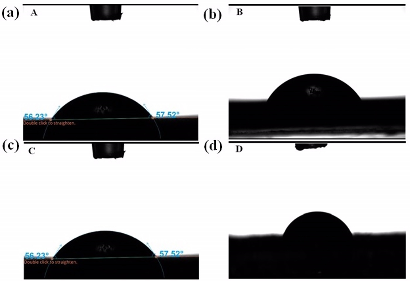
WCA of samples PbS: (a) A, (b) B, (c) C, and (d) D at 40 °C.
The WCAs of the PbS thin films obtained at 40 °C were obtained as A: 56.23°, B: 58.136°, C: 70.07°, and D: 69.734°, respectively (Figure 8).
4 Conclusions
According to the results of the XRD analysis, it was observed that CBD method was successful in the synthesis of PbS thin films. 40 °C was determined to be effective in coating the PbS on the smooth glass substrate. Especially, the syntheses performed at 40 °C were more efficient in obtaining nano-sized thin film at room conditions. The main Bragg peaks (2θ values) of the PbS construct were observed at 25.94°, 30.04°, 50.98°, 53.5°, 61.64°, 64.68° and 68.77° (d(111), (200), (220), (311), (222), (400), and (331)), respectively. It has been observed that the synthesis temperature and times cause changes in the crystal structures of nano-sized thin films. However, band gap values were not changed. It is predicted that the efficiency of the obtained PbS thin films in electro-photocatalytic reactions can be significantly improved with synthesis parameters.
Temperature and Na2S2O3 concentrations were also found to be influential for thin-film coating. As reaction time and concentration increased, so did the grain size of the PbS thin film. However, it was discovered that as the grain sizes increased, so did the number of pin-holes. This situation was found to be less effective in PbS thin films synthesized at 40 °C. Thin films obtained at 40 °C, low concentration, and low time, on the other hand, were much more homogeneous.
According to the obtained WCD results, it was observed that the temperature increase decreased the water contact angle. However, it was determined that the reaction accelerator had a reducing effect on the water contact angle at room conditions.
Acknowledgment
We would like to thank Burak Geyik, Oğuz Kaan Horoz, Dr. Nevin Atalay Gengeç and Ibrahim F. Balkaya.
-
Author contributions: All the authors have accepted responsibility for the entire content of this submitted manuscript and approved submission.
-
Research funding: None declared.
-
Conflict of interest statement: The authors declare no conflicts of interest regarding this article.
References
1. Milton, O. The Materials Science of Thin Films; Academic Press: San Diego, New York, Boston, 1992.Search in Google Scholar
2. AL-Rashdi, K., Farooqui, M., Mohsin, M., Rabbani, G. J. Adv. Sci. Res. 2016, 7, 01–08.Search in Google Scholar
3. Xu, J., Su, Y., Jia, L., Ma, L., Zhao, S. P. L., Liu, P., Wang, T., Hou, D. Characteristics of thin films of ferromagnetic semiconductor Fe1.1Ti0.9O3−δ under the pulsed laser deposition method at different substrate temperatures. J. Supercond. Nov. Magnetism 2022, 35, 851–856. https://doi.org/10.1007/s10948-021-06119-y.Search in Google Scholar
4. Popescu, V., Naşcu, H. I., Darvası, E. J. Optoelectron. Adv. Mater. 2006, 8, 1187–1193. https://doi.org/10.37358/Rev.Chim.1949.Search in Google Scholar
5. Seghaier, S., Kamoun, N., Brini, R., Amara, A. B. Mater. Chem. Phys. 2006, 97, 71–80. https://doi.org/10.1016/j.matchemphys.2005.07.061.Search in Google Scholar
6. Seghaier, S., Kamoun, N., Guasch, C., Zellama, K., Telmini, M., Mliki, N. T., Sediki, E. Fundamental and applied spectrometry. In AIP Conference Proceedings, Second International Spectroscopy Conference, ISC, Sousse, Tunisia, Vol. 935, 2007; pp. 143–148.10.1063/1.2795405Search in Google Scholar
7. Garcia, H. M., Gómez-Daza, O., Campos, J., Nair, M. T. S., Nair, P. K. Mater. Res. Soc. 2007, 1012, 451–456. https://doi.org/10.1557/PROC-1012-Y12-31.Search in Google Scholar
8. Gaiduk, A. P., Gaiduk, P. I., Larsen, A. N. Thin Solid Films 2008, 516, 3791–3795. https://doi.org/10.1016/j.tsf.2007.06.122.Search in Google Scholar
9. Kumar, D., Agarwal, G., Tripathi, B., Vyas, D., Kulshrestha, V. J. Alloys Compd. 2009, 484, 463–466. https://doi.org/10.1016/j.jallcom.2009.04.127.Search in Google Scholar
10. Pendyala, N. B., Rao, K. S. R. K. Mater. Chem. Phys. 2009, 113, 456–461. https://doi.org/10.1016/j.matchemphys.2008.07.125.Search in Google Scholar
11. González-Alfaro, Y., Fernández-Lima, F. A., Larramendi, E. M., Filho, H. D. F., Maia da Costa, M. E. H., Freire, F. L.Jr., Prioli, R., de Avillez, R. R., da Silveira, E. F., Calzadilla, O., de Melo, O., Pedrero, E., Hernández, E. Phys. Status Solidi C 2005, 10, 3690–3693. https://doi.org/10.1002/pssc.200461729.Search in Google Scholar
12. Yang, Y. J., Hu, S. Thin Solid Films 2008, 516, 6048–6051. https://doi.org/10.1016/j.tsf.2007.10.116.Search in Google Scholar
13. Majidi, F., Abedi, K., Pırsaraei, S. R. A. Iran, IJOH 2011, 38, 33–37.Search in Google Scholar
14. Hyugaji, M., Miura, T. Jpn. J. Appl. Phys. 1985, 24, 1575. https://doi.org/10.1143/JJAP.24.1575.Search in Google Scholar
15. Yadav, A. A., Barote, M. A., Masumdar, E. U. Mater. Chem. Phys. 2010, 121, 53–57. https://doi.org/10.1016/j.matchemphys.2009.12.039.Search in Google Scholar
16. Perna, G., Capozzi, V., Ambrico, M. Appl. Phys. 1998, 83, 3337. https://doi.org/10.1063/1.367102.Search in Google Scholar
17. Gruszeckix, T., Holmstrom, B. Mater. Solar Cell. 1993, 31, 227–234. https://doi.org/10.1016/0927-0248(93)90053-6.Search in Google Scholar
18. Boudreauand, R. A., Rauh, D. R. J. Electrochem. Soc. 1983, 13, 513. https://doi.org/10.1149/1.2119741.Search in Google Scholar
19. Reicman, J., Russak, M. A. Appl. Phys. 1982, 53, 708. https://doi.org/10.1063/1.329981.Search in Google Scholar
20. Sharma, S. K., Al-Kabbi, A. S., Saini, G. S. S., Tripathi, S. K. Mater. Res. Bull. 2012, 47, 1400–1406. https://doi.org/10.1016/j.materresbull.2012.03.008.Search in Google Scholar
21. Mandal, K. C., Savadogo, O. J. Mater. Sci. 1992, 27, 4355–4360. https://doi.org/10.1007/BF00541566.Search in Google Scholar
22. Mitzi, D. B. Solution Processing of Inorganic Materials; John Wiley & Sons: Hoboken, NJ, 2009; p. 512.10.1002/9780470407790Search in Google Scholar
23. Rempel, A. A., Kozhevnikova, N. S., Leenaers, A. J. G., Van den Berghe, S. J. Cryst. Growth 2005, 280, 300–308. https://doi.org/10.1016/j.jcrysgro.2005.03.005.Search in Google Scholar
24. Pentia, E., Pintilie, L., Botila, T., Pintilie, I., Chaparro, A., Maffiotte, C. Thin Solid Films 2003, 434, 162–170. https://doi.org/10.1016/S0040-6090(03)00449-8.Search in Google Scholar
25. Raniero, L., Ferreira, C., Cruz, L., Pinto, A., Alves, R. Phys. B Condens. Matter 2010, 405, 1283–1286. https://doi.org/10.1016/j.physb.2009.11.068.Search in Google Scholar
26. Hussain, A., Begum, A., Rahman, A. Arabian J. Sci. Eng. 2012, 38, 169–174. https://doi.org/10.1007/s13369-012-0390-3.Search in Google Scholar
27. Yeon, D., Lee, S., Jo, Y., Moon, J., Cho, Y. J. Mater. Chem. 2014, 2, 20112–20117. https://doi.org/10.1039/C4TA03433C.Search in Google Scholar
28. Kumaran, T. S., Banu, S. P. Int. J. Recent Sci. Res. 2013, 4, 1685–1687.Search in Google Scholar
29. Bhushan, S., Mukharjee, M., Bose, P. J. Mater. Sci.: Mater. Electron. 2002, 13, 581–584. https://doi.org/10.1023/A:1020196030287.Search in Google Scholar
30. Rajathi, S., Kirubavathi, K., Selvaraju, K. Arab. J. Chem. 2017, 10, 1167–1174. https://doi.org/10.1016/j.arabjc.2014.11.057.Search in Google Scholar
31. Koao, L., Dejene, F., Swart, H. Int. J. Electrochem. Sci. 2014, 9, 1747–1757.10.1016/S1452-3981(23)07888-4Search in Google Scholar
32. Yıldırım, A. K., Altıokka, B. Sakarya Univ. J. Sci. 2018, 22, 1500–1507. https://doi.org/10.16984/saufenbilder.409328.Search in Google Scholar
33. Contreras-Rascón, J. I., Díaz-Reyes, J., Luna-Suárez, S., Carrillo-Torres, R. C., Sánchez-Zeferino, R. Thin Solid Films 2019, 692, 137609. https://doi.org/10.1016/j.tsf.2019.137609.Search in Google Scholar
34. Önal, M., Altıokka, B. J. Nano Res. 2020, 63, 1–9. https://doi.org/10.4028/www.scientific.net/JNanoR.63.1.Search in Google Scholar
35. Altıokka, B. Arabian J. Sci. Eng. 2015, 40, 2085–2093. https://doi.org/10.1007/s13369-015-1680-3.Search in Google Scholar
36. Lincot, D., Hodes, G. Proceedings of the International Symposium; The Electrochemical Society, 2006; p. 235.Search in Google Scholar
37. Ubale, A. U., Junghare, A. R., Wadıbhasme, A. S., Daryapurkar, A. S., Mankar, R. B., Sangawar, V. S. Turk. J. Phys. 2007, 31, 279–286.Search in Google Scholar
38. Abdallah, B., Hussein, R., Al-Kafri, N., Zetoun, W. Iran. J. Sci. Technol. Trans. A Sci. 2019, 43, 1371–1380. https://doi.org/10.1007/s40995-019-00698-1.Search in Google Scholar
39. Barrios-Salgado, E., Rodríguez-Lazcano, Y., Pérez-Orozco, J. P., Colin, J., Altuzar, P., Campos, J., Quesada, D. Adv. Condens. Matter Phys. 2019, 2019, 1–8. https://doi.org/10.1155/2019/5960587.Search in Google Scholar
40. Zaragoza-Palacios, B. G., Torres-Duarte, A. R., Castillo, S. J. J. Mater. Sci.: Mater. Electron. 2021, 32, 22205–22213. https://doi.org/10.1007/s10854-021-06702-y.Search in Google Scholar
41. Karataş, C., Şimşek, V. Mater. Test. 2022, 64, 1860–1870. https://doi.org/10.1515/mt-2022-0124.Search in Google Scholar
© 2023 Walter de Gruyter GmbH, Berlin/Boston
Articles in the same Issue
- Frontmatter
- Original Papers
- Nanocrystalline PbS thin film produced by alkaline chemical bath deposition: effect of inhibitor levels and temperature on the physicochemical properties
- Effect of laser power on microstructure and tribological behavior of laser clad NiCr coating
- Mechanical characterization and evaluation of pitting corrosion resistance of a superferritic stainless steel model alloy 25Cr–6Mo–5Ni
- Factors dictating the extent of low elongation in high sulfur-containing bainitic steels
- Effect of process parameters on mechanical properties and wettability of polylactic acid by fused filament fabrication process
- Critical systematic investigation of the Cd–Ce system: phase stability and Gibbs energies of formation and equilibria via thermodynamic description
- Experimental study of the phase relations of the Fe–Pt–Ho ternary system at 500 °C
- Ultraviolet-B radiation from Gd (III) doped hardystonite
- Photoluminescence features of trivalent holmium doped Ca2La8(SiO4)6O2 phosphors
- Thermal stability of Al3BC3 powders under a nitrogen atmosphere
- News
- DGM – Deutsche Gesellschaft für Materialkunde