Simulation of the optical coating deposition
-
Fedor Grigoriev
Fedor Grigoriev is Senior Research Scientist of the Research Computing Center M. V. Lomonosov Moscow State University. He graduated from the Faculty of Theoretical and Experimental Physics at the National Research Nuclear University (MEPhi) in 1994. He obtained his PhD degree in Physical Chemistry from Kurnakov Institute of General and Inorganic Chemistry, Russian Academy of Sciences. He is an author of more than 50 publications. His research interests are the atomistic supercomputer simulation of the processes of the thin-film deposition, formation of the interatomic complexes in water, and formation of the point defects in solid phase.
 ,
Vladimir Sulimov
,
Vladimir Sulimov
Vladimir Sulimov is presently the Head of the laboratory of the Research Computing Center of Lomonosov Moscow State University, Moscow, Russia. He obtained his PhD degree in Mathematical and Theoretical Physics from Lomonosov Moscow State University and his Doctor of Sciences degree in Mathematical and Theoretical Physics from Prokhorov General Physics Institute of Russian Academy of Sciences. He is an author of more than 240 publications. His current research interests are in the application of molecular modeling to solving a broad spectrum of problems, including computer-aided structural-based drug design and thin optical film deposition modeling, application of Bayesian network technology to personalized medicine, and application of high-performance computing to these problems.
Alexander Tikhonravov is presently the Director of the Research Computing Center of Moscow State University, Moscow, Russia. He obtained his PhD degree and his Doctor of Sciences degree in Mathematical and Theoretical Physics from Moscow State University. He is an author of more than 350 publications. His current research interests are in thin-film optics, inverse problems, and application of high-performance computing to challenging technological problems.

Abstract
A brief review of the mathematical methods of thin-film growth simulation and results of their applications is presented. Both full-atomistic and multi-scale approaches that were used in the studies of thin-film deposition are considered. The results of the structural parameter simulation including density profiles, roughness, porosity, point defect concentration, and others are discussed. The application of the quantum level methods to the simulation of the thin-film electronic and optical properties is considered. Special attention is paid to the simulation of the silicon dioxide thin films.
1 Introduction
The first simulations of thin-film growth were performed more than 30 years ago [1], [2]. In these simulations, deposited atoms were considered as two-dimensional hard disks, and the substrate was represented as a strip consisting of the same disks as deposited ones. Despite its obvious simplicity, this model was able to qualitatively describe the structural properties of growing films, among them such important property as the columnar structure of thin film.
Because of the tremendous progress in high-performance computing, the simulation of thin-film growth gained a new interest in recent years. The atomistic simulation of optical layers having technologically sensible thicknesses of about a quarter of visible light wavelength is possible now using modern supercomputer facilities. The goal of this simulation is to provide insight onto dependencies of the film properties on deposition parameters such as deposited atom energy, substrate temperature, deposition rate, and angular distribution of the deposited atom flow.
In the simulation process, deposited films are represented by microscopic atomistic clusters. The numbers of atoms in these clusters and cluster dimensions are essentially dependent on the simulation approaches, which can be divided into quantum and classical ones. The most fundamental and time-consuming quantum chemistry (QC) simulation level is able to provide calculations of the optical and electronic properties of small clusters consisting of no more than several hundreds of atoms. Classical approaches provide calculation of structural and mechanical thin-film properties, but at the same time, they have a limited potential in optical property calculations because the light interaction with matter requires description at the quantum level.
The most essential features of the above-mentioned methods used for the simulation of thin-film growth and respective simulation software are considered in Sections 2 and 3, respectively. The applications of these methods, mainly classical molecular dynamics (MD), to the simulation of structural and mechanical thin-film properties are discussed in Sections 4 and 5. Simulations of optical and electronic thin-film properties are briefly considered in Sections 6. The final conclusions are given in Section 7.
2 Simulation methods
2.1 Input data for the simulation
In the classical simulation of the thin-film production, the following data are used as input data: parameters characterizing the beam of deposited particle parameters of the residual gas in a vacuum chamber, substrate temperature, etc. Unfortunately, such important input data as energy and velocity distributions of deposited particles and flux density are hardly available now for the most part of deposition processes.
There are two ways to handle this problem. The first one is based on the development of multi-scale models [3] that are able to simulate interactions of ion beam with target and resulting energy and velocity distribution of atoms arriving at the substrate. The second way is the investigation of the dependence of the simulation results on various parameters of the deposition process. In this case, the characteristic values of the deposition parameters should be taken from the intervals that are typical for the simulated deposition techniques. For instance, for the low-energy deposition techniques like thermal evaporation, the characteristic values of deposited particle energy should be taken around 0.1 eV, while for the high-energy techniques like ion beam sputtering (IBS), the energy of the sputtered atoms may achieve several tens of eV.
2.2 Classical molecular dynamics and Monte-Carlo methods
In frame of the full-atomistic approaches every atom of the simulation cluster is considered as a force center interacting with other atoms in accordance with the chosen expressions for the potential energy of interatomic interaction. In the case of MD simulation processes atoms of the growing film move accordingly to the Newton’s laws. In the case of Monte-Carlo (MC) method atoms move in agreement with the Metropolis scheme [4]. MD and MC algorithms are able to perform numerical experiments with millions of atoms and film thicknesses of more than hundred nanometers [5] at the modern high performance supercomputers. Time intervals of MD and MC modeling are limited by tens of nanoseconds and for this reason these modeling methods are not suitable for the simulation of such long-time processes as the surface diffusion. However, in the very recent years the combined MD and MC atomistic technique providing an essential acceleration of simulation was proposed [6]. In perspective this technique can be applied for optical coatings growth simulation.
Full-atomistic MD and MC approaches for deposition simulation are organized as a step-by-step procedure that, in general, consists of the following steps:
Deposited atoms are injected into random positions above the substrate surface (Figure 1). Initial velocities are directed to the substrate according to the angular distribution of the deposited atom velocities. Velocity values are specified accordingly to the energy distribution of the deposited particles, that is, either discrete [8], [10], [11], [12], [13], [14], [15] or continuous [3].
MD (MC) simulation starts from the described configuration. As a rule, the NVT (constant number of particles, volume, and temperature) ensemble with the periodic boundary conditions is used at this simulation step. Also, the NVE (constant number of particles, volume, and energy) ensemble is used for thermal equilibration before NVT simulation [3], [8].
Steps 2 and 3 are repeated until the growing film thickness achieves a specified value.

Simulation box structure.
This scheme was applied to the simulation of the silicon dioxide film deposition [7], [8], [10], [11], [12], [13], [14] as well as titanium dioxide [9], and other material [17] deposition.
The choice of the force field describing the interatomic interactions is one of the key issues in the classical atomistic simulation. Usually, the two-body interatomic potentials [18], [19], [20], [21], [22] are used for the thin-film growth simulation. In this case, the potential energy of the system is represented as the sum of terms depending on the distances between the pairs of interacting force centers. These terms are the electrostatic and the Van-der-Waals contributions. The first is the Coulomb interaction of point charges centered at the atoms. For the Van-der-Waals contribution, the Morse potential [23] was used for silica in Refs. [18], [19], [24], [25] and for TiO2 [26]. The Lennard-Jones potential was applied for the silicon dioxide thin-film simulation [10–14] as well as for Si-(ZrCu) films [27]. In Ref. [17], the pairwise ionic potential was applied to the study of the Mg–Al–O thin-film deposition.
More sophisticated many-body potentials [28], [29], [30], [31] were also used for the deposition process simulation [16]. The polarizable potentials were proposed to study the deposition of Tix Oy clusters with an impact energy of up to 40 eV onto a rutile substrate [32], [33].
The force field parameters are defined either from the quantum chemistry calculations [34], [35], [36] or from the fitting procedure comparing the calculated and experimental condense-phase properties. In Ref. [37], the ab initio-based force field was adapted for the condense-phase simulation and was applied for the simulation of the Ni film formation on the silicon dioxide substrate.
The universal ReaxFF force field based on the parameterization of the density functional theory (DFT) quantum chemistry calculations was developed in the recent year [38], [39], [40]. The ReaxFF has a functional form allowing one to describe the chemical bond formation and dissociation in terms of bond-order parameter depending on the interatomic distances. As the bond formation is an important component of the film growth process, the ReaxFF looks promising for the simulation of the deposition processes.
The following parameters are usually used in classical MD simulations of the silica deposition process [10], [11], [12], [13], [14], [15]: the time step of the MD modeling is 0.5 fs, duration of one deposition cycle (step 3 in the algorithm described in this section) is 4–6 ps for NVT simulation. The duration of the NVE simulation is equal 1 ps [8]. The Berendsen thermostat [41] is used to keep the simulation box temperature constant. The electrostatic component of the interatomic energy is calculated using the particle mesh Ewald [42] method.
2.3 Kinetic Monte Carlo
In the above section, we joined discussions of the MD and MC methods because both methods have similar thermodynamic background and describe processes at the same level of sophistication. The kinetic Monte Carlo (kMC) stays separately and requires specifying the transition rates between the initial and possible final states of the system. These rates should be obtained from the results of the simulation using other methods such as MD and MC, mentioned in Section 2.2.
The kMC approach is specially oriented to the simulation of rare events. This approach is not accurate enough for the description of fast processes such as collisions of high-energy deposited atom with the substrate and the film, but it is suitable for the simulation of long-time processes like the diffusion of deposited atoms on the growing film surface. The kMC algorithms are able to simulate the processes having a duration of hundreds and thousands of seconds in the clusters consisting of millions of atoms [43], [44].
The kMC was applied for the simulation of Cu thin film growth [45], [46]. The diffusion of atoms on the growing surface was taken into account in the frame of the applied model. The Morse potential was used for the calculation of interatomic potential energy with parameters that are defined in Refs. [24], [47]. The film density dependence on the substrate temperature was investigated in Ref. [45]. The multi-scale approach including the kMC simulation level was developed in Ref. [3] and was applied for the simulation of TiO2 thin-film deposition. The density and roughness dependencies on the number of deposited atoms were investigated. In these simulation experiments, the maximum number of deposited atoms achieved two million.
2.4 Quantum methods
The QC approaches are used for the simulation of optical and electronic thin-film properties. As the QC modeling requires a lot of computational recourses, the simulation cluster dimensions are essentially smaller than those in the case of the MD simulations (Figure 2). The atomic positions in the QC cell should be optimized before the optical and electronic parameter calculations.

Comparison of the QC and classical MD simulation levels.
In Ref. [3], the quantum chemistry approach was applied for the optical property calculation of the resulting classical MD TIO2 films. The stoichiometric TIO2 supercell structure consisting of 96 atoms was prepared from the deposited film. All simulations were performed using the Vienna ab initio simulation package [48]. The electronic correlation and the exchange interaction were considered at the density functional theory level [49] in the frames of the PBE generalized gradient approximation [50] and the hybrid functional HSE06 [51].
The self-consistent charge density-functional-based tight-binding (DFTB) method was used in Ref. [52] for the simulation of the highest occupied molecular orbital–lowest unoccupied molecular orbital (HOMO–LUMO) gap and the electronic density of the states of the TIO2 clusters.
2.5 Other methods
In Ref. [53], the simplified approach referred to as the discrete approach was proposed. This approach describes the growing film as a set of sites that can be either empty or occupied by atoms [53]. The discrete approach is suitable for simulations of crystalline substrate and films. Several models of the deposition process – random, ballistic, and solid on solid – were considered [53]. In the frames of these models, every injected atom was deposited at a random position of a regular network representing the film surface. The models differ by equations describing the height dependence of a network site on the deposition time. In the simplest case of random deposition without diffusion, the model has an analytical solution predicting the unlimited surface roughness growth with the increase in the number of deposited atoms.
In Ref. [54], the simulation of the SiO2 thin-film deposition was performed based on the assumption that silicon oxidation on the growing film surface can be described in terms of Brownian motion (three-dimensional random walk) of oxygen atoms. The probability of oxygen atoms moving from one local minimum to another was calculated as exp(−E/kBT), where E is the activation energy. Moving was performed if the probability was greater than a random value in the interval [0; 1]. This scheme is close to the Metropolis algorithm that is widely used in MC simulations.
The dependence of the nanostructured TiO2 film thickness on the deposition conditions was studied with the help of the artificial neural network (ANN) and regression method [26]. The ANN was used to determine the relationships between the deposition parameters and the deposited film properties. The author of Ref. [26] concluded that the application of the ANN in combination with MD simulations allows one to reduce the number of experiments.
2.6 Interface between different theory levels
One of the main tasks of the thin-film growth modeling is providing a proper interface between the different simulation levels. The problem is that the most accurate QC level providing the calculations of the key thin-film parameters (refractive index, electronic density gap, and so on) can be applied only to small clusters consisting of no more than several hundreds of atoms. The concept of the virtual coater [55] was proposed to solve the problem. The idea is to combine simulation techniques having different length scales to a multiple scale model. The corresponding approach is outlined in Ref. [55]. The vacuum chamber geometry, ion source, and target parameters were the input data for the first simulation level. The output of this level (deposited atom energy and velocity distribution, density of their flow, charges of the deposited atoms, and so on) were then used as the input data for the classical simulation approaches: MD, MC, and kMC. The structural parameters (density, point defect concentration, porosity, and structural ring distribution) can be used to prepare the simulation cells for the QC level. The first results of the application of this scheme in studying titanium oxide films is presented in Ref. [3].
3 Software for the thin-film growth simulation
The software for the film growth simulation should be chosen taking into account its potential for reproducing the main features of a real deposition process: injections of deposited atoms, atomic collisions with a film and substrate-film interface, formation of transition layers between film and vacuum, and specific boundary conditions.
The quantum molecular dynamics simulations of the structural, electronic, and optical properties of deposited film can be performed using the Vienna Ab Initio Simulation Program (VASP) (University of Vienna, Faculty of Physics, Vienna, Austria) [48]. The many-body quantum problem can be considered in the VASP in the frame of the density function theory, Hartree-Fock approximation, and perturbation theory (second-order Møller-Plesset). At the same time, a direct simulation of the deposition process in the VASP requires an adequate description of the transition layer between condense matter and vacuum.
The large-scale atomic/molecular massively parallel simulator (LAMMPS) (Sandia National Laboratories, US Department of Energy laboratory, Livermore, CA, USA) (http://lammps.sandia.gov/) is suitable for the thin-film growth simulation using the classical MD approach. The LAMMPS provides step-by-step injections of the deposited atoms into the simulation area. Different pairwise and polarizable force fields are implemented in the LAMMPS.
Groningen machine for chemical simulations (GROMACS) (Department of Biophysical Chemistry, University of Groningen, Groningen, Netherlands) [56], Not another molecular dynamics program (NAMD) (Beckman Institute of the University of Illinois, Urbana-Champaign, CA, USA) (http://www.ks.uiuc.edu/), and DLPOLY (A general-purpose parallel molecular dynamics simulation package) [Science and Technology Facilities Council (STFC), Daresbury, UK] [57] software packages can be also used for the thin-film deposition simulation on the classical atomistic level despite the fact that both programs were initially oriented to the organic molecule modeling. All mentioned programs are well paralleled and can be installed on the supercomputers.
Simulations at the kMC level can be performed using the three-dimensional kinetic Monte Carlo code nanoscale modeling (NASCAM) (University of Namur, Department of Physics, Namur, France) (http://www.unamur.be/sciences/physique/pmr/telechargement/logiciels/nascam). This code was specially developed for the simulation of deposition, diffusion, nucleation, and growth of films.
4 Structural properties
4.1 Density
The results of the silicon dioxide density calculations using the classical MD simulations with different force fields are summarized in Table 1.
Density ρ (g/cm3) of silicon dioxide glassy and thin films.
| Glassy | ||||||||
| ρ | 2.18 [34] | 2.21 [18] | 2.58 [21] | 2.3a [35] | 2.2a [58] | 3.0a,b [59] | 2.42a [30] | 2.14 [10] |
| Films | ||||||||
| E | 0.1 | 1 | 5 | 10 | ||||
| ρ | 2.06 | 2.29, 1.95 [8] | 1.98 [8] | 2.41, 2.1 [8] | ||||
| ρc | 2.03 | 2.2 | 2.25 | |||||
It is seen from Table 1 that the most part of the applied force fields reproduce the experimental value of the silicon dioxide glassy density (this value is equal to 2.2 g/cm3). It is likely that the high density value of 2.58 g/cm3 reported in Ref. [58] for the Beest Kramer and van Santen (BKS) force field [21] is connected with the BKS fitting scheme that is oriented to the calculations of the crystalline cell parameters.
Simulations of the thin-film deposition processes in the frame of the deposited films of silica (DESIL) force field [10–14] show that the deposited film density is somewhat higher than the density of glassy silica. These simulations also show that the film density is higher when the energy of the deposited silicon atoms is higher.
Thermal annealing results in the essential reduction of the densities of the deposited SIO2 films (see the bottom row of Table 1). This result is in a good agreement with the experimental data [60].
The density profiles of the deposited silicon dioxide films are shown in Figure 3. Simulations were performed in the frame of the DESIL force field for the three different values of silicon atom energy. Silica glass substrate was prepared from α-quartz by heating it from 300 K to the temperature above the quartz melting point followed by quenching in the MD simulation with GROMACS [56]. Every deposition cycle was simulated in the NVT (constant number of atoms, volume, and temperature) ensemble. The deposition temperature was equal to 300 K, and the initial velocities of the oxygen atoms corresponded to 0.1 eV. Essential fluctuations of the film density were observed in the case of low-Si atom energy. The increase in deposition energy results in a smoother density profile.

Density profiles of the deposited SiO2 films.
The density profiles of the silicon dioxide thin films for the temperature values in the interval from 3400 K to 5200 K are reported in Ref. [61]. The BKS force field [21] was used for the simulation. The maximum cluster size in Ref. [61] achieved 2.7 nm. The density fluctuations with amplitudes up to 0.2 g/cm3 were observed. The thickness of the transition layer between the film and vacuum achieved 0.5–0.7 nm.
The dependence of the TIO2 film density on the number of deposited atoms was investigated in Ref. [3] using the kMC approach. The MA pairwise potential [31], including the Coulomb and Buckingham terms, was used. It was found that the density reduces with the growth of the deposited atom number N (the N values of up to ~106 were considered). It was also found that the density reduces from 3.4 to 2.7 g/cm3 with the growth of incidence angle from 0° to 50° in the case of the TI atom energy of 0.1 eV. The density increased approximately for 0.6 g/cm3 when the TI atom energy was increased from 0.1 eV to 10 eV [3].
4.2 Roughness
In Ref. [62], the surface roughness was calculated as a root mean square deviation of the vertical coordinates of the surface atoms. The surface roughness of the deposited TIO2 films was calculated in Ref. [3] using the kMC approach. In all the cases, the roughness was increased with the growth of the number of the deposited atoms, and it achieved 1.5 nm for N=2 · 106. The roughness was also increased with the growth of the angle of incidence. It was reduced from 1.3 nm to 0.2 nm with an increase in the deposited Ti atom energy from 0.1 eV to 10 eV (angle of incidence equal to zero).
The dependence of the roughness Rh on the SIO2 thin-film thickness and deposition conditions was investigated in the frame of the DESIL force field in Refs. [10], [11], [12], [13], [14]. To calculate Rh, the horizontal plane of the simulation box was divided into square cells having the same surface areas (see Figure 4). For every cell, a search for the atom with a maximum vertical coordinate hi was performed.

Dependencies of thin-film roughness on film thickness for various energies of deposited Si atoms E(Si) and different substrate temperatures T.
The Rh value was then calculated as a rms of the hi values. The calculated Rh values were in a good agreement with the experimental data [63]. It is seen from Figure 4 that the decrease in the substrate temperature results in the increase in the Rh values in the case of the silicon atom energy of 0.1 eV. The growth of the deposition energy leads to a reduction in the surface roughness.
The theoretical models of the evolution of the surface characteristics including the roughness characteristics are discussed in Ref. [53]. The horizontal plane of the growing film was divided into cells. The equations describing the time dependence of the film height in the frame of every cell were derived. The model taking into account surface diffusion was applied in studying the diamond-like carbon film growth. It was found that the increase in the deposition energy leads to the decrease in the surface roughness.
4.3 Porosity and point defects
The porosity analysis of the TiO2 films was performed in Refs. [3], [44]. The kMC approach was used to obtain a film cluster consisting of two million deposited atoms. Only the pores that were able to contain at least 15 atoms were taken into account. It was found that the closed pores were located near the growing film surface, and this was considered as the evidence of a rather dense structure of the film. The total volume of all the closed pores having diameters of at least two atomic dimensions was found to be equal to 7% of the total cluster volume. The pore concentration rapidly decreased with the pores size growth.
The porosity of the silicon dioxide films was studied in the frame of the classical MD simulation using the DESIL force field in Refs. [10], [11], [12], [13], [14]. The number of the deposited atoms in the simulation procedure achieved 2.4 · 105.
Only the pores having dimensions of at least 0.1 nm were taken into account. It is seen from Figure 5 that low deposition energy results in the formation of pores with dimensions of up to several nanometers. These pores are not observed in the case of high deposition energy. The concentration of the pores for all dimensions is reduced with the growth of the deposition energy.

Pores in the SIO2 films atomistic structure. Values of the deposited Si atom energies are shown.
The simulation of the point defects in the silicon dioxide thin films and fused silica was performed in Ref. [14]. It was found that the main types of point defects in SiO2 were one- and three-coordinated oxygen atoms O1 and O3. The concentrations of these defects were calculated for the two films deposited at different energies of the deposited Si atoms. The influence of annealing on the point defect concentration was also studied. The results are shown in Figure 6. The defect concentration in the ‘as-deposited’ films is higher in the case of low deposition energy. The annealing procedure results in the essential reduction of the point defect concentration for all defect types and for all deposition energies.
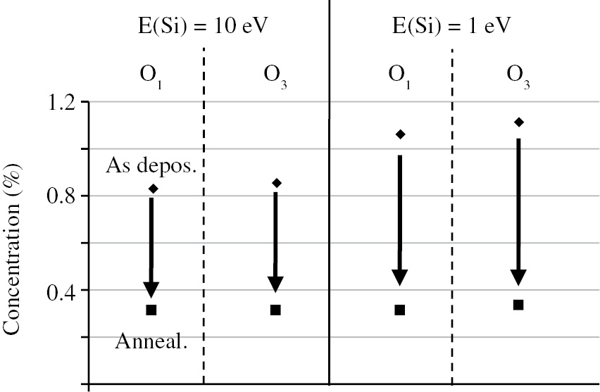
Point defect concentration in ‘as-deposited’ and annealed SIO2 films.
4.4 Ring statistics
Rings consisting of different numbers of atoms (n-membered rings) are formed in different compounds (SiO2, TiO2, B2O3, and so on). The relative weights of the n-membered rings is defined as fn=Nn/Ntot, where Nn is the number of the n-membered rings and Ntot is the total number of rings.
The relative weights for the different n were calculated for the deposited SiO2 films using the MD approach with the DESIL force field. The crystalline silicon dioxide consists of only six- and eight-membered rings, while in the fused silica and SiO2 films, rings with different n values are formed. Values of fn were calculated using the shortest path analysis [64].
The results of the ring statistic calculations are shown in Figure 7. The geometry of the chemical bonds is strained in the rings with n<5 as the values of the interatomic Si–O distances and the valence angles O–Si–O differ from the equilibrium ones. The most strained structure is formed in the case of the low substrate temperature and low energy of the deposited Si atoms.

Ring statistic for different deposition conditions.
The obtained distributions of the fn values are in agreement with the experimental results for the fused silica [65], [66]. The detailed comparison of the fn distribution for the different force fields is performed in Ref. [67]. For all the force fields, the distribution maximum corresponds to the six-membered ring. The relative weight of the strained rings (N<5) is minimal in the case of the Tersoff potential for SiO2 [30].
5 Mechanical properties
The Classical MD (MC) simulation enables one to study such important thin-film properties as its stress. The tensile and compressive types of stress are schematically shown at the top of Figure 8; their values have positive and negative signs, respectively. Stress can be calculated using the diagonal components of the pressure tensor pxx, pyy at the boundaries of the modeling box (the film grows in the z direction). These components are calculated based on the difference of the kinetic energies of the system and its virial. The values of pxx and pyy are averaged over the MD trajectories in the NVT (constant number of particles, volume, and temperature) ensemble with T=300 K after the deposition process is finished. The diagonal components of the stress tensor σxx(yy) are calculated as σxx(yy)=−pxx(yy).

Dependencies of the stress on film thickness for different energies E of deposited Si atoms and substrate temperatures T.
The results of the stress simulation for silicon dioxide thin films using the DESIL force field are shown in Figure 8. Only the average values of the horizontal plane diagonal stress component σ= (σxx+σyy)/2 are presented because the differences between σxx and σyy are small for all the values of film thickness.
In all cases, the compressive stress is observed. In the case of the deposited Si atom energy E=10 eV, the absolute stress value is several times larger than in the case of E=0.1 eV. The growth of the substrate temperature results in the reduction of stress in the case of E=10 eV. The calculated stress values are in a good agreement with the experimental data [68].
The value of the mechanical loss in thin films is the limiting factor for high-precision gravitational wave detectors and optical devices that are used in the laser interferometer gravitational-wave observatory project. The two-well model is used to calculate the dependence of the mechanical loss in optical coatings on temperature and frequency in amorphous pure and doped silica [69] and amorphous tantala and titania-doped tantala [70]. The functional form of the interatomic potential energy was corresponded to the BKS potential [21] with an additional Morse term. The force field parameters were fitted to repro duce the radial distribution functions and elastic constants. The low-temperature peaks in the loss of pure and doped tantala were reproduced in the simulation.
6 Optical and electronic properties
The dependence of the electronic HOMO-LUMO gap of the amorphous TiO2 on the mass density was investigated in Ref. [16] using the DFTB approach [52] and the VASP quantum molecular dynamics program [48]. It was found that the gap decreases almost linearly with the increase in the mass density.
The dependencies of the refractive index n on the energy of the TiO2 supercell and on the number of atoms in the supercell are studied in Ref. [9]. It was found that n increases with the growth of energy. The calculated value of n was less than the experimental one for 0.2 in the visible spectral range.
The densities of the deposited silicon dioxide films are higher than the fused silica density (see Table 1). This results in the respective growth of n. The difference Δn between the refractive indexes of the film and the glassy SIO2 was estimated using the Gladstone-Dale equation [71] in the form Δn=0. 21·Δρ, where Δρ is the difference between the film and glassy density. For the ‘as-deposited’ film at E(Si)=10 eV, the value of Δn achieves 0.05. The annealing procedure results in the essential reduction of Δρ and, respectively, of Δn. The values of the densities and refractive indices that were obtained by the MD simulation with the DESIL force field are in agreement with the experimentally reported values [72].
The experimental verification of the validity of the SiO2 deposition simulation is performed in Ref. [73]. The refractive index dependence on the wavelength is shown in Figure 9. It is seen that the refractive index difference between the glassy silicon dioxide and the SiO2 film is close to 0.04 for all wavelengths in the considered diapason. This result corresponds to the calculated Δn value in the case of the deposited Si atom energy 10 eV.

Experimental dependencies of the refractive index on wavelength for the silicon dioxide glassy and deposited film.
7 Conclusion
The methods of the simulation of the structural, mechanical, electronic, and optical properties of the deposited films are discussed. Special attention is paid to the atomistic simulation, as quantum as classical. The classical molecular dynamic modeling of the structural and mechanical film properties is considered in detail. The simulation results relating to the dependencies of film density, point defect concentration, stresses, surface roughness, porosity, refractive index, and gap in the density of the electronic states on the deposition conditions are observed. Application of the considered approaches to the simulation of silicon dioxide film deposition is discussed in detail. The increase in the energy of the deposited Si atoms results in the increase in the silica film density and the decrease in the porosity and the growth of absolute values of compressive stress.
About the authors

Fedor Grigoriev is Senior Research Scientist of the Research Computing Center M. V. Lomonosov Moscow State University. He graduated from the Faculty of Theoretical and Experimental Physics at the National Research Nuclear University (MEPhi) in 1994. He obtained his PhD degree in Physical Chemistry from Kurnakov Institute of General and Inorganic Chemistry, Russian Academy of Sciences. He is an author of more than 50 publications. His research interests are the atomistic supercomputer simulation of the processes of the thin-film deposition, formation of the interatomic complexes in water, and formation of the point defects in solid phase.
Vladimir Sulimov is presently the Head of the laboratory of the Research Computing Center of Lomonosov Moscow State University, Moscow, Russia. He obtained his PhD degree in Mathematical and Theoretical Physics from Lomonosov Moscow State University and his Doctor of Sciences degree in Mathematical and Theoretical Physics from Prokhorov General Physics Institute of Russian Academy of Sciences. He is an author of more than 240 publications. His current research interests are in the application of molecular modeling to solving a broad spectrum of problems, including computer-aided structural-based drug design and thin optical film deposition modeling, application of Bayesian network technology to personalized medicine, and application of high-performance computing to these problems.

Alexander Tikhonravov is presently the Director of the Research Computing Center of Moscow State University, Moscow, Russia. He obtained his PhD degree and his Doctor of Sciences degree in Mathematical and Theoretical Physics from Moscow State University. He is an author of more than 350 publications. His current research interests are in thin-film optics, inverse problems, and application of high-performance computing to challenging technological problems.
Acknowledgments
The reported study was funded by RSF according to the research project No. 14-11-00409, Funder Id: 10.13039/501100006769. The research is carried out using the equipment of the shared research facilities of the HPC computing resources at Lomonosov Moscow State University.
References
[1] M. Sikkens, I. J. Hodgkinson, F. Horowitz, H. A. Macleod and J. J. Warton, Proc. SPIE 505, 236 (1984).10.1117/12.964652Search in Google Scholar
[2] M. Sikkens, I. J. Hodgkinson, F. Horowitz, H. A. Macleod and J. J. Wharton, Opt. Eng. 25, 142 (1986).10.1117/12.7973791Search in Google Scholar
[3] M. Turowski, M. Jupé, T. Melzig, P. Moskovkin, A. Daniel, et al., Thin Solid Films 592, 240 (2015).10.1016/j.tsf.2015.04.015Search in Google Scholar
[4] N. Metropolis and S. Ulam, J. Am. Stat. Assoc. 44, 335 (1949).10.1080/01621459.1949.10483310Search in Google Scholar PubMed
[5] F. Grigoriev, A. Sulimov, I. Kochikov, O. Kondakova, V. Sulimov, et al., Optical Interference Coatings (OIC) 2016 © OSA 2016. WB.5.pdf10.1364/OIC.2016.WB.5Search in Google Scholar
[6] E. C. Neyts and A. Bogaerts, in: ‘Theoretical Chemistry in Belgium. Highlights in Theoretical Chemistry’, Eds. By B. Champagne, M. Deleuze, F. De Proft and T. Leyssens, vol 6. (Springer, Berlin, Heidelberg, 2014).Search in Google Scholar
[7] M. Taguchi and S. Hamguchi, Jpn. J. Appl. Phys. 45 (10B), 8163 (2006).10.1143/JJAP.45.8163Search in Google Scholar
[8] M. Taguchi and S. Hamaguchi, Thin Solid Films 515, 4879 (2007).10.1016/j.tsf.2006.10.097Search in Google Scholar
[9] M. Turowski, T. Amotchkina, H. Ehlers, M. Jupé and D. Ristau, Appl. Opt. 53, A159 (2014).10.1364/AO.53.00A159Search in Google Scholar PubMed
[10] F. V. Grigoriev, A. V. Sulimov, I. V. Kochikov, O. A. Kondakova, V. B. Sulimov, et al., Int. J. High Perform. Comp. Appl. 29, 184 (2015).10.1177/1094342014560591Search in Google Scholar
[11] F. Grigoriev, Moscow University Physics Bulletin 70, 521 (2015).10.3103/S0027134915060107Search in Google Scholar
[12] F. V. Grigoriev, A. V. Sulimov, I. V. Kochikov, O. A. Kondakova, V. B. Sulimov et al., Proc. SPIE. 9627, 962708 (2015).10.1117/12.2190938Search in Google Scholar
[13] F. V. Grigoriev, A. V. Sulimov, E. V. Katkova, I. V. Kochikov, O. A. Kondakova, et al., J. Non-Cryst. Solids 448, 1 (2015).10.1016/j.jnoncrysol.2016.06.032Search in Google Scholar
[14] F. V. Grigoriev, E. V. Katkova, A. V. Sulimov, V. B. Sulimov, I. V. Kochikov, et al., Opt. Mater. Exp. 6, 3960 (2016).10.1364/OME.6.003960Search in Google Scholar
[15] F. Grigoriev, A. Sulimov, I. Kochikov, O. Kondakova, V. Sulimov, et al., Appl. Opt. 56, C87 (2017).10.1364/AO.56.000C87Search in Google Scholar
[16] T. Köhler, M. Turowski, H. Ehlers, M. Landmann, D. Ristau, et al., J. Phys. D: Appl. Phys. 46, 325302 (2013).10.1088/0022-3727/46/32/325302Search in Google Scholar
[17] V. Georgieva, M. Saraiva, N. Jehanathan, O. I. Lebelev, D. Depla, et al., J. Phys. D: Appl. Phys. 42, 065107 (2009).10.1088/0022-3727/42/6/065107Search in Google Scholar
[18] A. Takada, P. Richet, C. R. A. Catlow and G. D. Price, J. Non-Cryst. Solids 345, 224 (2004).10.1016/j.jnoncrysol.2004.08.247Search in Google Scholar
[19] N. T. Huff, E. Demiralp, T. Cagin and W. A. Goddard III, J. Non-Cryst. Solids 253, 133 (1999).10.1016/S0022-3093(99)00349-XSearch in Google Scholar
[20] T. Soules, G. H. Gilmer, M. J. Matthews, J. S. Stolken and M. D. Feit, SPIE 2010 Boulder, 1–34 (2010) (digital.library.unt.edu/ark:/67531/metadc871862/).Search in Google Scholar
[21] B. W. H. van Beest, G. J. Kramer and R. A. van Santen. Phys. Rev. Lett. 64, 1955 (1990).10.1103/PhysRevLett.64.1955Search in Google Scholar
[22] C. R. A. Catlow, C. M. Freeman and R. L. Royle, Physica B and C 131, 1 (1985).10.1016/0378-4363(85)90134-2Search in Google Scholar
[23] P. M. Morse, Phys. Rev. 34, 57 (1929).10.1103/PhysRev.34.57Search in Google Scholar
[24] H. N. G. Wadley, X. Zhou and R. A. Johnson, Prog. Mater. Sci. 46, 329 (2001).10.1016/S0079-6425(00)00009-8Search in Google Scholar
[25] V. V. Hoang, N. T. Hai and H. Zung, Phys. Lett. A 356, 246 (2006).10.1016/j.physleta.2006.03.052Search in Google Scholar
[26] A. Bahramian, Surf. Interface Anal. 45, 1727 (2013).10.1002/sia.5314Search in Google Scholar
[27] L. Xie, P. Brault, J.-M. Bauchire, A.-L. Thomann and L. Bedra, J. Phys. D: Appl. Phys. 47, 224004 (2014).10.1088/0022-3727/47/22/224004Search in Google Scholar
[28] F. H. Stillinger and T. A. Weber, Phys. Rev. B 31, 5262 (1985).10.1103/PhysRevB.31.5262Search in Google Scholar PubMed
[29] H. Ohta and S. Hamaguchi, J. Chem. Phys. 115, 6679 (2001).10.1063/1.1400789Search in Google Scholar
[30] S. Munetoh, T. Motooka, K. Moriguchi and A. Shintani, Comput. Mater. Sci. 39, 334 (2007).10.1016/j.commatsci.2006.06.010Search in Google Scholar
[31] M. Matsui and M. Akaogi, Mol. Simul. 6, 239 (1991).10.1080/08927029108022432Search in Google Scholar
[32] L. J. Vernon, R. Smith and S. D. Kenny, Nucl. Instrum. Methods B 267 3022 (2009).10.1016/j.nimb.2009.06.093Search in Google Scholar
[33] L. J. Vernon, S. D. Kenny and R. Smith, Nucl. Instrum. Methods B 268, 2942 (2010).10.1016/j.nimb.2010.05.014Search in Google Scholar
[34] Y. Yu, B. Wang, M. Wang, G. Sant and M. Bauch, J. Non-Cryst. Solids 443, 148 (2016).10.1016/j.jnoncrysol.2016.03.026Search in Google Scholar
[35] A. Carre, J. Horbach, S. Ispas and W. Kob. EPL 82, 17001 (2008).10.1209/0295-5075/82/17001Search in Google Scholar
[36] D. Corradini, Y. Ishii, N. Ohtori and M. Salanne. Modelling Simul. Mater. Sci. Eng. 23, 074005 (2015).10.1088/0965-0393/23/7/074005Search in Google Scholar
[37] Y. Maekawa and Y. Shibuta, Chem. Phys. Lett. 658, 30 (2016).10.1016/j.cplett.2016.06.016Search in Google Scholar
[38] C. T. Adri van Duin, A. Strachan, S. Stewman, Q. Zhang, X. Xu, et al., J. Phys. Chem. A 107, 3803 (2003).10.1021/jp0276303Search in Google Scholar
[39] C. T. Adri van Duin, S. Dasgupta, F. Lorant and W. A. Goddard, III. J. Phys. Chem. A 105, 9396 (2001).10.1021/jp004368uSearch in Google Scholar
[40] C. T. Adri van Duin, J. M. A. Baas and B. van de Graaf. J. Chem. Soc., Faraday Trans. 90, 2881 (1994).10.1039/ft9949002881Search in Google Scholar
[41] H. J. C. Berendsen, J. P. M. Postma, W. F. van Gunsteren, A. DiNola and J. R. Haak. J. Chem. Phys. 81, 3684 (1984).10.1063/1.448118Search in Google Scholar
[42] T. Darden, D. York and L. Pedersen. J. Chem. Phys. 98, 10089 (1993).10.1063/1.464397Search in Google Scholar
[43] S. Lucas and P. Moskovkin, Thin Solid Films 518, 5355 (2010) (NASCAM available for downloading at http://www.unamur.be/sciences/physique/pmr/telechargement/logiciels/nascam).10.1016/j.tsf.2010.04.064Search in Google Scholar
[44] V. Godinho, P. Moskovkin, R. Alvarez, J. Caballero-Hernandez, R. Schierholz, et al., Nanotechnology 25, 355705 (2014).10.1088/0957-4484/25/35/355705Search in Google Scholar PubMed
[45] Z. Peifeng, Z. Xiaoping and H. Deyan, Sci. China (Series G) 46, 610 (2003).Search in Google Scholar
[46] M. Pomeroy, J. Joachim and C. Colin, Phys. Rev. B 66, 235412-1 (2002).10.1103/PhysRevB.66.235412Search in Google Scholar
[47] H. L. Wei, Z. L. Liu and K. L. Yao, Vacuum 56, 185 (2000).10.1016/S0042-207X(99)00193-1Search in Google Scholar
[48] G. Kresse and J. Furthmüller. Comput. Mater. Sci. 6, 15 (1996).10.1016/0927-0256(96)00008-0Search in Google Scholar
[49] P. Hohenberg, Phys. Rev. 136, B864 (1964).10.1103/PhysRev.136.B864Search in Google Scholar
[50] J. P. Perdew, K. Burke and M. Ernzerhof, Phys. Rev. Lett. 77, 3865 (1996).10.1103/PhysRevLett.77.3865Search in Google Scholar
[51] J. Heyd, G. E. Scuseria and M. Ernzerhof, J. Chem. Phys. 118, 8207 (2003).10.1063/1.1564060Search in Google Scholar
[52] M. Elstner, T. Frauenheim and S. Suhai, J. Mol. Struct. (Theochem) 632, 29 (2003).10.1016/S0166-1280(03)00286-0Search in Google Scholar
[53] F. L. Forgerini and R. Marchiori, Biomatter 4, e28871 (2014).10.4161/biom.28871Search in Google Scholar
[54] E. F. da Silva and B. D. Stosi, Semicond. Sci. Technol. 12, 1038 (1997).10.1088/0268-1242/12/8/018Search in Google Scholar
[55] M. Turowski, M. Jupé, H. Ehlers, T. Melzig, A. Pflug, et al., Proc. SPIE 9627, 962707 (2015).10.1117/12.2191693Search in Google Scholar
[56] H. J. C. Berendsen, D. van der Spoel and R. van Drunen, Comput. Phys. Commun. 91, 56 (1995).10.1016/0010-4655(95)00042-ESearch in Google Scholar
[57] W. Smith and T. Forester, J. Mol. Graph. 14, 136 (1996).10.1016/S0263-7855(96)00043-4Search in Google Scholar
[58] T. F. Soules, G. H. Gilmer, M. J. Matthews, J. S. Stolken and M. D. Feit, J. Non-Cryst. Solids 357, 1564 (2011).10.1016/j.jnoncrysol.2011.01.009Search in Google Scholar
[59] V. V. Hoang, J. Phys. Chem. B 111, 12649 (2007).10.1021/jp074237uSearch in Google Scholar
[60] K. Taniguchi, M. Tanaka, C. Hamaguchi and K. Imai, J. Appl. Phys. 67, 2195 (1990).10.1063/1.345563Search in Google Scholar
[61] A. Roder, W. Kob and K. Binder, J. Chem. Phys. 114, 7602 (2001).10.1063/1.1360257Search in Google Scholar
[62] E. S. Gadelmawla, M. M. Koura, T. M. A. Maksoud, I. M. Elewa and H. H. Soliman, J. Mater. Process. Technol. 123, 133 (2002).10.1016/S0924-0136(02)00060-2Search in Google Scholar
[63] F. Elsholz, E. Schöll, C. Scharfenorth, G. Seewald, H. J. Eichler, et al., J. Appl. Phys. 98, 103516 (2005).10.1063/1.2130521Search in Google Scholar
[64] X. Yuan and A. N. Cormack, Comput. Mater. Sci. 24, 343 (2002).10.1016/S0927-0256(01)00256-7Search in Google Scholar
[65] Y. Tu and J. Tersoff, Phys. Rev. Lett. 84, 4393 (2000).10.1103/PhysRevLett.84.4393Search in Google Scholar PubMed
[66] V. M. Burlakov, G. A. D. Briggs, A. P. Sutton and Y. Tsukahara, Phys. Rev. Lett. 86, 3052 (2001).10.1103/PhysRevLett.86.3052Search in Google Scholar PubMed
[67] S. von Alfthan, A. Kuronen and K. Kaski, Phys. Rev. B 68, 073203 (2003).10.1103/PhysRevB.68.073203Search in Google Scholar
[68] W. J. Fang, Micromech. Microeng. 9, 230 (1999).10.1088/0960-1317/9/3/303Search in Google Scholar
[69] R. Hamdan, J. P. Trinastic and H. P. Cheng, J. Chem. Phys. 141, 054501 (2014).10.1063/1.4890958Search in Google Scholar PubMed
[70] J. P. Trinastic, R. Hamdan, C. Billman and H.-P. Cheng, Phys. Rev. B 93, 014105 (2016).10.1103/PhysRevB.93.014105Search in Google Scholar
[71] K. Vedam and P. Limsuwan, J. Chem. Phys. 69, 4772 (1978).10.1063/1.436530Search in Google Scholar
[72] Y. Jiang, H. Liu, L. Wang, D. Liu, C. Jiang, et al., Appl. Opt. 53, A83 (2014).10.1364/AO.53.000A83Search in Google Scholar PubMed
[73] V. G. Zhupanov, F. V. Grigoriev, V. B. Sulimov and A. V. Tikhonravov, Mosc. Univ. Phys. Bull. 72, (2017).10.3103/S0027134917060248Search in Google Scholar
©2018 THOSS Media & De Gruyter, Berlin/Boston
Articles in the same Issue
- Cover and Frontmatter
- Editorial
- Reviewer recognition and editor’s note
- Community
- News
- Topical Issue: Optical Coatings
- Editorial
- Special issue on optical coatings
- Review Article
- Simulation of the optical coating deposition
- Research Articles
- ALD anti-reflection coatings at 1ω, 2ω, 3ω, and 4ω for high-power ns-laser application
- Determination of refractive index and thickness of YbF3 thin films deposited at different bias voltages of APS ion source from spectrophotometric methods
- Effects of fixture rotation on coating uniformity for high-performance optical filter fabrication
- Design and manufacture of super-multilayer optical filters based on PARMS technology
- Tutorial
- Monolithic photonic integration for visible and short near-infrared wavelengths: technologies and platforms for bio and life science applications
- Review Articles
- Optimization of freeform surfaces using intelligent deformation techniques for LED applications
- On-chip photonic microsystem for optical signal processing based on silicon and silicon nitride platforms
- Letter
- On-chip Mach-Zehnder interferometer for OCT systems
- Research Article
- Broadband and scalable optical coupling for silicon photonics using polymer waveguides