A MEMS-based gas sensor for H2S detection with enhanced performance using a Ni–In2O3/ZnO nano-composite
-
Cui Chen
 ,
Yang Zhao
,
Yang Zhao

Abstract
A micro-electro-mechanical system (MEMS) gas sensor based on a Ni–In2O3/ZnO nano-composite for detecting hydrogen sulfide gas (H2S) was constructed. The sensitive nano-material is applied onto a hot plate to create a MEMS gas sensor. X-ray diffraction (XRD), X-ray photoelectron spectroscopy (XPS), and scanning electron microscopy (SEM) were employed to examine the crystal structure, elemental composition, and surface morphology of the fabricated Ni–In2O3/ZnO gas composite film. The sensitive material has a dense porous surface morphology and is uniformly coating the MEMS device. The coating on the MEMS microheater exhibits high selectivity and a sensitivity of 3.4 ± 0.12 μA ppm−1 to H2S, maintaining strong linear behavior. Additionally, the response duration is 4.4 s, while the recovery period is 5.2 s. With superior responsiveness, precise targeting, stable performance, and repeatable outcomes, this device opens new avenues for creating cost-effective and high-performance solutions for future H2S sensing.
1 Introduction
MEMS (micro-electro-mechanical system) 1 , 2 gas sensors are high-precision, miniaturized sensors manufactured using micro-nano technology and are widely used in environmental monitoring, industrial safety, medical diagnosis and other fields. Its core advantages are small size, low power consumption, fast response speed, and easy integration. It can monitor harmful gases or specific gas concentrations in the air.
Traditional sensing techniques 3 , 4 – such as electrochemical, optical, or catalytic combustion methods – often suffer from limitations like large size, high power consumption, slow response, and poor stability. In contrast, micro-electro-mechanical systems (MEMS)-based gas sensors 5 have attracted growing interest due to their miniaturization, low power consumption, rapid response, high sensitivity, and potential for mass production.
MEMS sensors typically incorporate metal oxide semiconductors (MOS) as the active sensing layer, where Hydrogen sulfide (H2S) is detected through variations in electrical conductivity resulting from surface chemical reactions. H2S is a hazardous, highly flammable, and corrosive gas commonly encountered in industrial production, wastewater treatment, and landfill sites. 6 Exposure to 100 ppm 7 of H2S may lead to poisoning within an hour, threatening both human health and environmental safety. Due to these dangers, accurate detection and real-time monitoring of H2S gas are vital.
To meet these needs, the development of sensitive, selective, and reliable H2S sensors is essential. The performance of these sensors is highly dependent on the material’s structure, morphology, and composition. As a result, current research focuses on optimizing MOS materials and microfabrication techniques to enhance the overall sensing performance, including sensitivity, selectivity, stability, and repeatability.
In2O3, 8 , 9 a key metal oxide semiconductor in gas sensors, is valued for its thermal stability, conductivity, and chemical properties. However, it fails for H2S detection, showing low response, high detection limits, and slow response times. Increasing surface oxygen vacancies can help to address these issues. Zinc oxide (ZnO) 10 boasts a broad 3.4 eV bandgap and a strong 60 meV exciton binding energy at ambient conditions. With adaptable electronic traits, flexible shapes, and a large surface-to-volume ratio, it excels in catalytic activities and finds broad usage in devices like light detectors, gas monitoring systems, and catalytic converters.
However, individual metal oxide sensors typically have poor gas sensitivity. Composite materials improve this sensitivity and introduce unique properties. When two semiconductor oxides form a heterojunction, differences in their Fermi levels cause carrier transfer, creating a space charge layer essential for enhanced sensitivity. This heterojunction approach using metal oxide nano-materials is now widely applied. Qin 11 and his team in 2020, engineered a nano-structure composed of ZnO and SnO2, incorporating an n-n heterojunction. This structure features abundant mesopores distributed between 2 and 13 nm. Under a temperature of 240 °C, nano-sheets with a 3:1 Zn/Sn molar ratio showed an ethanol gas response of 80, nearly tenfold higher compared to pure ZnO. However, there have been no reports on the use of Ni–In2O3/ZnO materials for gas sensing.
This research utilized the hydrothermal technique to synthesize In2O3/ZnO 12 nano-composites, and then Ni doping was achieved using a high-temperature solid-state method to obtain Ni–In2O3/ZnO. The MEMS gas sensor was prepared by coating multiple layers of stacked Ni–In2O3/ZnO on a micro-hotplate using the spin-coating method. By observing the changes in the current-time curve on the electrochemical workstation, effective monitoring of H2S gas concentration was achieved, and the gas sensitivity performance was systematically analyzed.
2 Principle
2.1 Sensing principle
Figure 1(a) displays the experimental arrangement for the MEMS-based H2S gas sensor. In this study the sensor consists of a digital power supply (DP 100), an electrochemical workstation (CH Instruments), a MEMS sensor chip, a gas chamber, and the reacting gases (hydrogen sulfide and other reactant gases) to form a MEMS gas sensing system. One end of the MEMS chip is connected to the digital power supply (DP 100), and the other end is connected to the CHI760E Shanghai Chenhua electrochemical workstation (CH Instruments) for real-time monitoring of electrical signals. In Figure 2(a), the gas sensor chip is displayed in the Nexcope NE700 series microscope. The lens uses a HAYEAR 4K USB 3.0 camera. The size of the MEMS gas sensor chip is 1 × 1 mm. The gas chamber of the gas sensor is made of 2 mm thick acrylic material, and the internal volume is 10 × 5 × 5 cm3, as shown in Figure 2(b). The MEMS gas sensor device is shown in Figure 2(c). The internal structure of the chip used in this experiment has a support layer, a sensitive film, two sets of electrodes, one set of heating electrodes and one set of test electrodes. The sensitive film prepared in this experiment is spin-coated on the top layer, as shown in Figure 2(d).
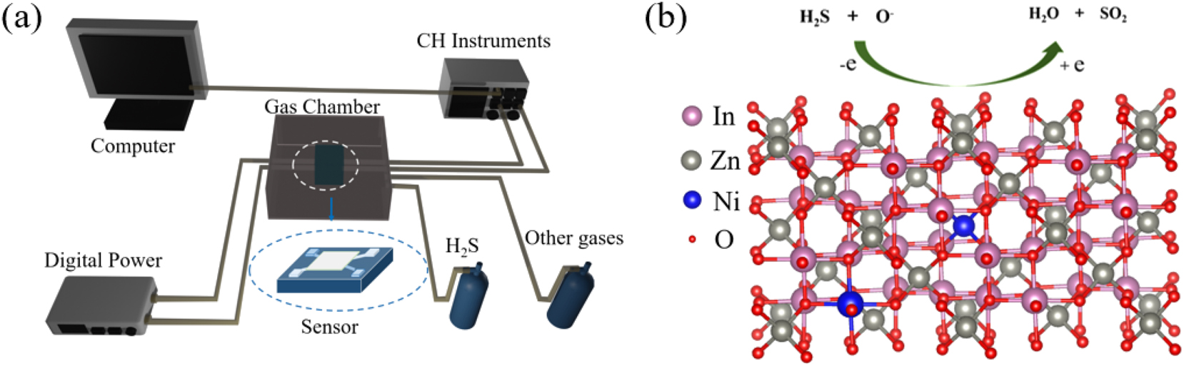
The gas sensor system. (a) MEMS sensor H2S monitoring experimental device diagram, (b) gas sensing mechanism of Ni–In2O3/ZnO.
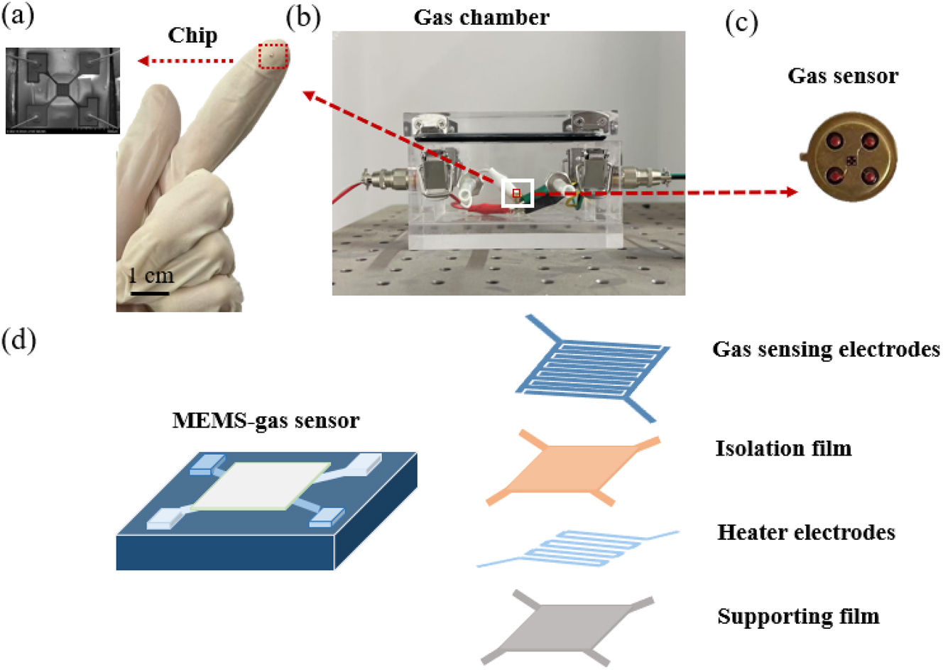
MEMS sensor with (a) the MEMS chip, (b) the air chamber, (c) the gas sensor device, and (d) internal structure of the chip.
The fundamental structure of this sensor comprises a MEMS microheater and a resistor composed of Ni–In2O3/ZnO nano-multistage heterostructured nano-materials. The microheater is made using MEMS technology, capable of providing a constant temperature to boost both the sensitivity and the stability of the sensor. In2O3/ZnO 11 heterostructured nano-materials are synthesized using the hydrothermal method, followed by Ni doping to finally produce Ni–In2O3/ZnO, which serves as the sensitive layer for the sensor. The sensitive material is uniformly spin-coated on the MEMS microheater and then placed in a gas chamber for gas experiments. When the target gas enters the sensor, it adsorbs onto or reacts with the Ni–In2O3/ZnO nano-sensitive film, altering the concentration and mobility of carriers (electrons or holes) on the surface or in the volume, thus changing the resistance. 13
The working principle 14 , 15 of resistive semiconductor sensors is as follows: upon air exposure, the surface of the Ni–In2O3/ZnO nano-wires becomes coated with oxygen atoms from the surrounding environment. This reaction reduces oxygen vacancies on the ZnO nano-wires, lowering the surface carrier concentration and increasing the resistance. The amount of oxygen adsorbed varies with the sensor’s operating temperature due to oxygen’s high electron affinity. At 300 °C, the oxygen adsorbed as O−, tends to withdraw electrons from the material’s surface, resulting in a charge depleted layer on the Ni–In2O3/ZnO surface (Equations (1) and (2)). 14 , 15 The depletion of electrons causes the barriers at the interfaces between nearby oxide particles to thicken, which subsequently enhances the resistance of the sensor material. As a result, in the presence of air, the sensor maintains an elevated resistance (Ra) state. When H2S, a reducing agent, is introduced into the chamber, it chemically reacts with the oxygen ions bound to the sensor’s surface. Oxygen adsorbed via chemisorption releases trapped electrons into the material, causing surface electrons to re-enter their conduction bands (Equations (3) and (4)), 15 thereby reducing the sensor’s resistance Rg).
For sensor fabrication, the Ni–In2O3/ZnO heterojunction is specifically utilized to detect hydrogen sulfide (H2S) as shown in Figure 1(b). When gas molecules react with the oxygen bonded to the heterojunction, electrons previously held on the surface are freed and return to the conduction bands. This leads to a reduction in particle boundary barriers, a shallower electron depletion zone, and a swift drop in the sensor’s overall resistance. 15 When the reducing gas is present, the resistance (Rg) greatly decreases, significantly enhancing the sensing response.
3 Experimental section
3.1 Preparation of the sensing materials In2O3 and ZnO
To prepare In2O3 nano-materials, a solution was created by gradually adding 0.5 g of indium nitrate, 0.3 g of sodium citrate, and 0.1 g of urea into 40 mL of purified water, ensuring constant agitation with a magnetic stirrer. After complete dissolution, a clear and homogeneous solution was obtained, which was then transferred to a 100 mL Teflon-lined autoclave for hydrothermal treatment at 200 °C for 20 h. The solid product was extracted by centrifugation, rinsed with ethanol several times, and dried thoroughly. Subsequently, the material was heated at 500 °C for 3 h with a controlled temperature increase of 3 K min−1, producing high-quality In2O3 nano-material. 15
For the preparation of ZnO, 7.44 g (0.025 mol) of zinc nitrate hexahydrate and 2.94 g (0.0132 mol) of sodium citrate were dissolved in 20 mL of distilled water with magnetic stirring (4 rpm) for 100 min to achieve a clear and homogeneous solution. Aqueous sodium hydroxide solution was introduced drop by drop, maintaining stirring until the solution’s pH was adjusted to 13. The mixture was then placed into a Teflon-lined autoclave and heated at 150 °C for 12 h. After cooling to ambient temperature, the solid material was isolated through centrifugation, rinsed four times with ethanol to eliminate remaining impurities, and dried at 80 °C for 5 h. The dried product was annealed at 200 °C for 3 h, with a controlled temperature increase of 5 K min−1, yielding ZnO powder characterized by excellent crystallinity and purity. 16
3.2 Preparation of the sensing material Ni–In2O3/ZnO
All chemicals used in this study were of analytical grade. 0.5 mmol of indium nitrate In(NO3)3 · xH2O and 1 mmol of zinc nitrate Zn(NO3)2 · 6H2O were dissolved in a mixed solvent of 30 mL glycerol and 50 mL isopropanol (3:5 v/v) under vigorous stirring for 30 min. Then, the mixture was transferred into a 100 mL PTFE-lined reactor and subjected to the hydrothermal reaction at 180 °C for a duration of 6 h. The reaction mixture was taken out of the autoclave and allowed to air-cool to ambient temperature. The precipitate was centrifuged and rinsed three times with deionized water and pure ethanol. Finally, the material was dried at 80 °C for 1 h to acquire the In/Zn-glycerate precursor which was calcined at 350 °C at a heating rate of 2 K min−1 for 3 h to form the In2O3/ZnO heterostructure. 17 1 mmol (74.69 mg) of the NiO was ground it together with In2O3/ZnO in a natural agate mortar for 3 h. After sieving through a 300-mesh screen, the mixed powder is placed into an alumina crucible and heated at 800 °C for 2 h to synthesize the Ni–In2O3/ZnO nano-material.
3.3 Characterization
The crystal structure analysis was conducted using a Bruker D8 ADVANCE X-ray diffractometer, set at 40 mA tube current and 40 kV tube voltage, with Cu and Co targets emitting wavelengths of 1.5406 and 1.79026 Å, respectively. The elemental composition of the nano-particles was examined through X-ray photoelectron spectroscopy (XPS) using a Thermo Escalab 250XI from Thermo Fisher Scientific. The system has a monochromatic AlKα source (hν = 1,486.6 eV) at 150 W, with a 650 µm beam spot, 14.8 kV voltage, and a 1.6 A current. To correct for charge, the C1s peak of surface carbon contamination at 284.8 eV was used. The sample surfaces were studied using a HITACHI S-4800 field emission SEM to investigate their morphological characteristics. Elemental analysis was conducted with the HORIBA EMAX mics2 system, utilizing acceleration voltages of 3 or 5 kV and achieving a resolution of 50 nm. The broad scan was performed using a 100 eV pass energy and a 1 eV step size, whereas the fine scan applied a 20 eV pass energy with a 0.1 eV step size. All tests were conducted at ambient temperature.
3.4 MEMS gas sensing characteristics
The sensitive material was mixed with deionized water (DI) in a 4:1 ratio by weight and ground in an agate mortar to produce a paste. Using a micropipette, the mixture was placed onto the micro-hotplate, air-dried at ambient temperature, and subsequently aged in a vacuum oven. The aging temperature was stabilized at 350 °C for 2 days. The sensing component was subjected to a 500 °C heat treatment for 2 h, removing the bound water and forming a compact oxide layer on the gas sensor’s surface, ultimately producing the MEMS sensor. Once cooled, a CNC power supply was used to power the electrodes, ensuring that the micro-hotplate reached the required reaction temperature. To evaluate the sensor’s electrical behavior, an instrument for gas sensing analysis (model CHI760E, manufactured by Shanghai Chenhua) was employed. During the test, the testing device was placed in a fume hood. The target gas, combined with dry air, was injected into the chamber and left to diffuse, ensuring complete exposure to the sensitive surface of the chip over a set period. The CHI760E software was then opened to begin testing the I–T curve. Response and recovery times refer to the intervals required for the sensor to attain 90 % of the complete current shift during the phases of gas adsorption and desorption. The operating temperature of the sensor was 300 °C.
4 Results and discussion
4.1 Crystal structure
Figure 3 presents the XRD patterns of In2O3, ZnO, In2O3/ZnO, and Ni–In2O3/ZnO, along with their simulated reference patterns. The diffraction peaks of In2O3 correspond to a cubic bixbyite structure (space group Ia
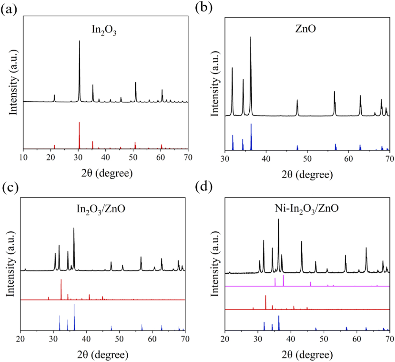
The XRD patterns of (a) In2O3, (b) ZnO, (c) In2O3/ZnO and (d) Ni–In2O3/ZnO.
The In2O3/ZnO composite displays combined diffraction peaks from both In2O3 and ZnO, with no evidence of new phases, indicating good phase compatibility. In the Ni–In2O3/ZnO sample, additional peaks were observed, corresponding to the cubic NiO phase (space group Fm
These results confirm the coexistence of In2O3, ZnO, and NiO in the doped composite. No unexpected or unidentified peaks were detected, supporting the phase purity and structural integrity of the synthesized materials.
4.2 Compositions
Figure 4(a) presents the XPS spectra of In2O3, ZnO and the In2O3/ZnO composite, while Figure 4(b) shows the In 3d peaks of In2O3 and In2O3/ZnO, Figure 4(c) the Zn 2p peaks of ZnO and In2O3/ZnO, and Figure 4(d) the O 1s peaks of In2O3, ZnO and In2O3/ZnO.
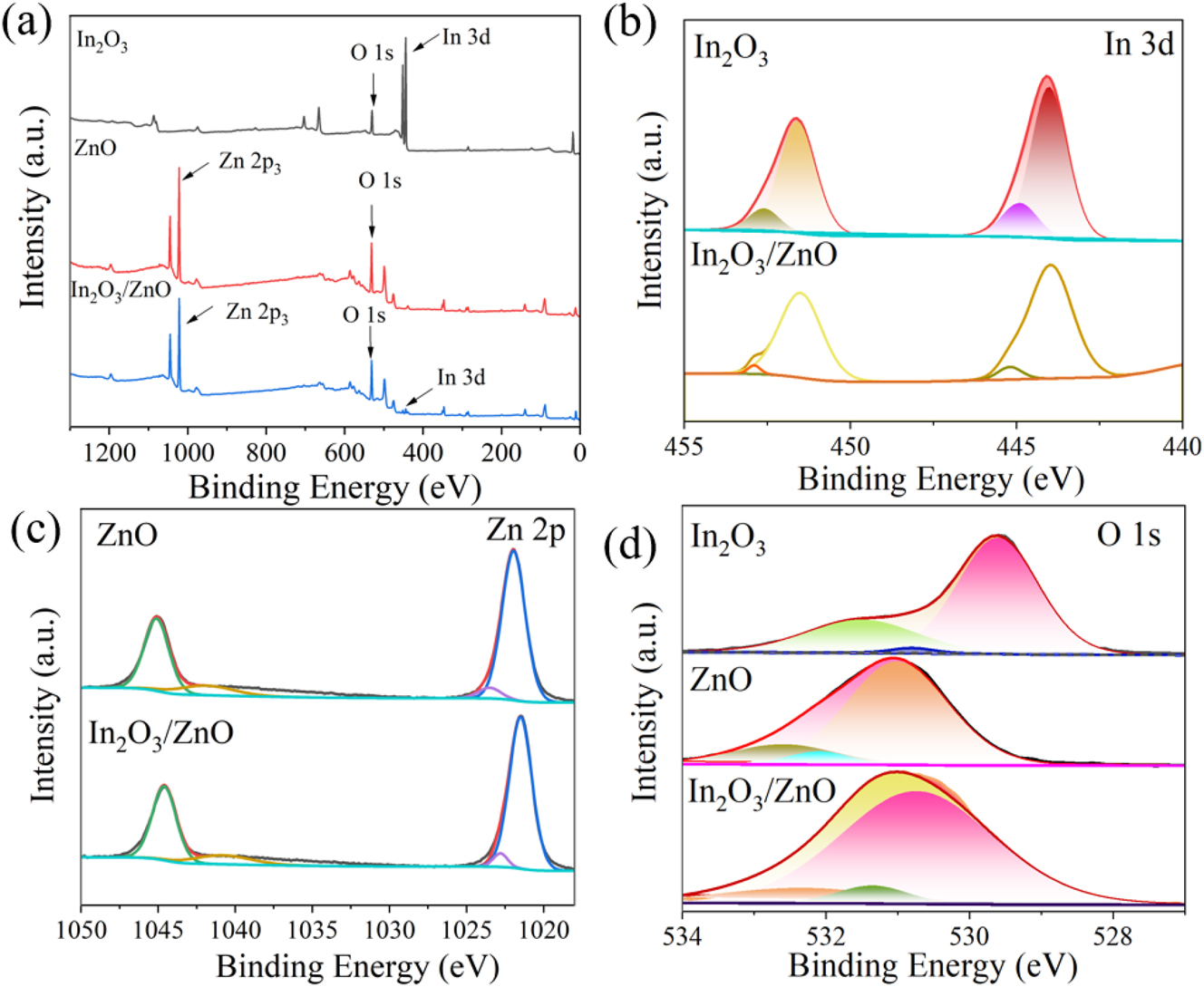
The XPS spectrum. (a) The XPS full-scan images of In2O3, ZnO and In2O3/ZnO, (b) the 3d regions of In2O3 and In2O3/ZnO, (c) the Zn 2p regions of ZnO and In2O3/ZnO, (d) the O 1s regions of In2O3, ZnO and In2O3/ZnO.
Figure 5(a) presents the XPS spectrum of the Ni–In2O3/ZnO composite. The analysis of the spectrum confirms that the composite contains the elements nickel (Ni), indium (In), zinc (Zn), and oxygen (O). The C 1s peak 22 is attributed to organic carbon contamination or trace amounts of glycerol that are not fully decomposed in the composite (Figure 5(b)). Binding energies of 854.40 eV and 873.11 eV are assigned to Ni 2p 3/2 and Ni 2p 1/2 23 (Figure 5(c)). The low doping levels result in weak peak intensities, accompanied by satellite peaks at 861.36 and 879.16 eV. As demonstrated in Figure 5(d), the fitted Zn 2p peaks reveal binding energies of 1,044.3 and 1,022.2 eV, which align with Zn 2p 1/2 and Zn 2p 3/2, respectively. Based on previous studies, 24 the In 3d peaks, shown in Figure 5(e), are identified as follows: 444.60 eV represents the In 3d 5/2 peak, while 452.18 eV is attributed to In 3d 3/2 peak. To determine the exact proportion of chemisorbed oxygen, the O 1s peak 25 was analyzed through XPS testing. As shown in Figure 5(f), the deconvolution of the O 1s peak reveals three distinct peaks at binding energies of 529.8 eV (OⅢ), 530.5 eV (OⅡ), and 531.8 eV (OⅠ). The OⅠ peak corresponds to lattice oxygen, while the OⅡ peak is linked to adsorbed oxygen. The binding energy at OⅡ (Oc) is typically attributed to chemisorbed or dissociated oxygen. 26 In resistive gas sensors, oxygen chemisorption on the material surface is critical, as it governs both the redox interactions between gas molecules and oxygen species, along with the gas adsorption and desorption mechanisms.
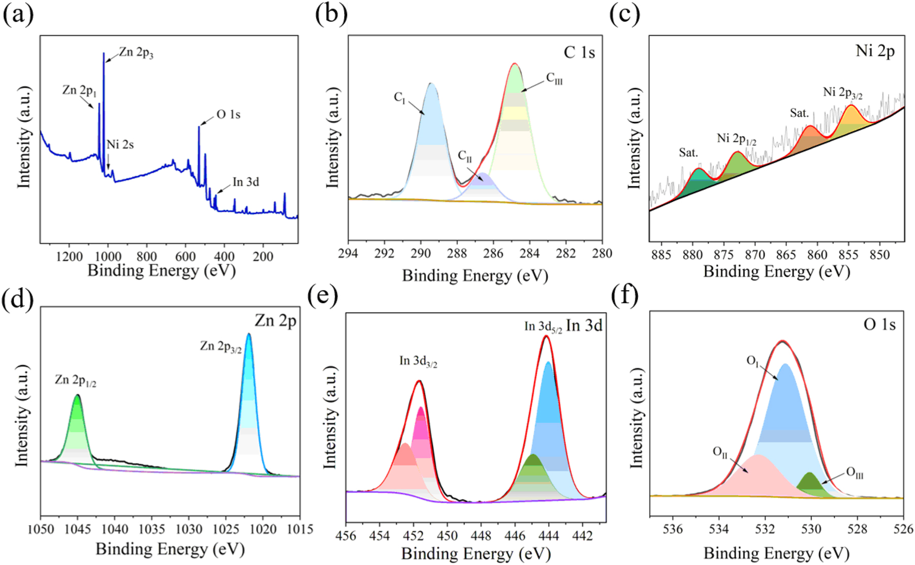
The XPS spectrum of Ni–In2O3/ZnO. (a) XPS full-scan images of Ni–In2O3/ZnO, (b) the C 1s region, (c) the Ni 2p region, (d) the Zn 2p region, (e) the Sn 3d 5/2 region, (f) the O 1s region.
4.3 Morphology
The SEM images of indium oxide are shown in Figure 6(a)–(c). From Figure 6(c), it can be seen that the crystals of indium oxide are in a cube-like shape. 18 The images of zinc oxide are presented in Figure 6(d)–(f), and Figure 6(f) shows that zinc oxide is present in the form of flakes. The images of indium oxide/zinc oxide are shown in Figure 6(g)–(i), where Figure 6(i) illustrates that the granular objects are attached to the flaky material. The SEM images of the sensor material, shown in Figure 6(j)–(l), show the Ni–In2O3/ZnO morphology at magnifications of 20×, 50×, and 100×. At 100× magnification, the surface of the sensor material is clearly visible. The microscope images reveal irregular small droplet shapes with inconsistent sizes, in a loose and porous structure. The size of the smallest irregular spherical grains is mainly in the range of 100–250 nm in diameter. The grain boundaries are distinct, and the surface is relatively smooth. The presence of gaps between the blocks facilitates gas adsorption and desorption. 27
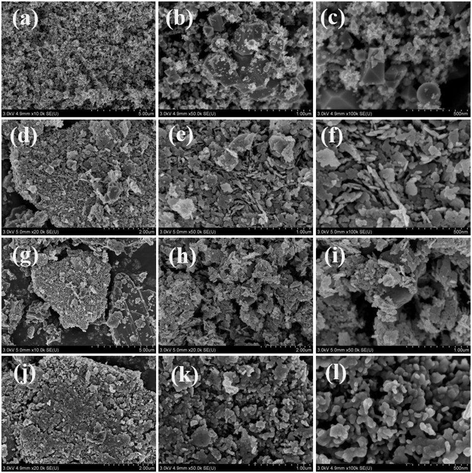
Figures (a), (b) and (c) show the FE-SEM images of In2O3, figures (d), (e) and (f) the FE-SEM images of ZnO, figures (g), (h) and (i) the FE-SEM images of the In2O3/ZnO sensing film, and figures (j), (k) and (l) the FE-SEM images of Ni–In2O3/ZnO.
Elemental distribution maps of the Ni–In2O3/ZnO material are illustrated in Figure 7(a)–(e), showing that the synthesized Ni–In2O3/ZnO consists solely of the intended elements, with no impurities present. Figure 4(f) shows the EDS spectrum of Ni–In2O3/ZnO.
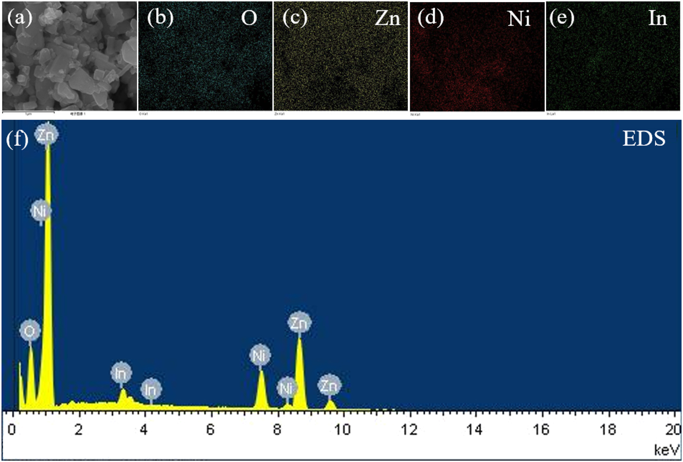
The SEM image. (a) The HAADF image of Ni–In2O3/Zn, the mapping images of (b) O, (c) Zn, (d) Ni and (e) In. Figure (f) shows the EDS spectrum of Ni–In2O3/ZnO.
4.4 Gas sensing
The gas sensor prepared in this work was tested with four different sensing materials under 100 ppm concentration of hydrogen sulfide gas. As shown in Figure 8, the response of Ni–In2O3/ZnO to hydrogen sulfide gas is the highest. Therefore, this material is chosen as the sensing film for this study.
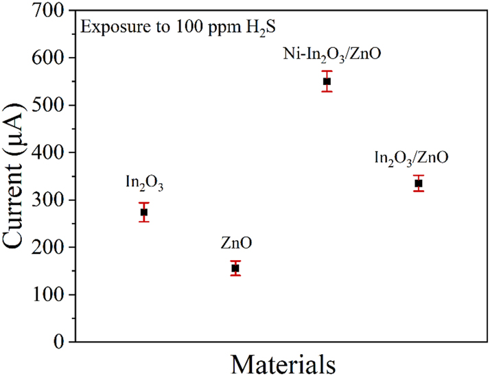
The gas sensor testing of different materials under 100 ppm hydrogen sulfide conditions.
At an operating temperature of 300 °C, the Ni–In2O3/ZnO nano-materials were tested under a broad range of hydrogen sulfide gas concentrations. The tested gas concentrations were 0, 20, 50, 80, and 100 ppm. In Figure 9(a), the sensor’s reaction patterns to differing levels of hydrogen sulfide gas concentrations are illustrated. An increase in test gas concentration leads to a corresponding rise in the response output of the MEMS sensor covered with the sensitive material. The MEMS gas sensor achieved the best sensitivity to H2S at 3.4 ± 0.12 μA ppm−1, indicating a linearity of 0.90201, as shown in Figure 9(b).
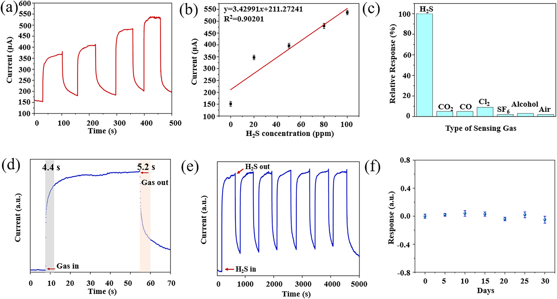
The gas sensor testing of (a) the gas sensitivity response curve of the MEMS sensor for different concentrations of H2S, (b) the linear fitting image, (c) the selectivity of the Ni–In2O3/ZnO MEMS senor towards H2S, CO2, CO, Cl2, SF6, ethanol and air, (d) the response and recovery time of the Ni–In2O3/ZnO micro-hotplate sensor, (e) the reproducibility of the Ni–In2O3/ZnO MEMS sensor for H2S at 50 ppm, (f) the stability of the gas sensor.
By performing a linear analysis of the experimental data using Origin, the standard deviation (δ) was obtained, and the detection threshold (LOD) of the gas sensor was computed, with K being the slope of the linear fit. The LOD of the sensor is, 28
The calculated limit of detection for the MEMS gas sensor can reach 0.57 ppm.
To examine how the coated MEMS sensor responds to different gases with cross-sensitivity, gases with equal concentrations of H2S, CO2, CO, Cl2, SF6, ethanol, and air were prepared and introduced into the gas chamber. Figure 9(c) presents the gas selectivity chart for the Ni–In2O3/ZnO sensor. It demonstrates minimal sensitivity when exposed to the tested gases such as CO2, CO, Cl2, SF6, ethanol, and air at the same concentration, indicating that Ni–In2O3/ZnO exhibits specific selectivity for H2S gas.
The response-recovery behavior of the sensor is depicted in Figure 9(d). Measurements were conducted at 0.1 s intervals, and random time points were selected for measuring the response time. Repeated measurements of the sensor’s response and recovery times were conducted to remove inaccuracies caused by manual computations. With a response time of approximately 4.4 s and a recovery time of 5.2 s, the sensor exhibits a quick reaction, considerably faster than the sensors referenced in Table 1. 29 , 30 , 31 , 32 , 33 , 34 , 35
Comparison of the response and recover time for different H2S sensors.
| Material | Temperature (°C) | H2S | T res (s) | T rec (s) | Ref. |
|---|---|---|---|---|---|
| MOF-derived Co3O4 | 250 | 100 ppm | 63.56 | 103.34 | 29] |
| CuO/CeO2 | 180 | 100 ppm | 39 | – | 30] |
| MoO3/MnO2 (MM-10) | RT | 1,000 ppb | 40 | 42 | 31] |
| In2O3 | 27 | 5 ppm | 18 | 507 | 32] |
| 5α-Fe2O3/NiO | 300 | 20 ppm | 38 | 35 | 33] |
| Ag–SnO2 | 28 | 10 ppm | 5 | 8 | 34] |
| ZnO NCs/F-GaNa | 220 | 50 ppm | 78 | 31 | 35] |
| Ni–In2O3/ZnO | 300 | 100 ppm | 4.4 | 5.2 | This work |
-
aFoam-like GaN. 35
Figure 9(e) shows the reproducibility of sensors with different parameters in 100 ppm H2S gas. For a single sensor, the relative standard deviation of the reproducibility, or sensitivity error should not exceed ±5 %. Since the reproducibility error of the Ni–In2O3/ZnO MEMS sensor meets this standard, it indicates that the sensor has relatively good reproducibility. The stability of the MEMS gas sensor was evaluated over a span of 30 days. Every 5 days, the sensor’s response value in a 50 ppm hydrogen sulfide gas environment was measured. As seen in Figure 9(f), the results reveal minor variations in response, confirming the consistent performance of the Ni–In2O3/ZnO gas sensor over both short and extended periods, which underscores its suitability for real-world market usage.
5 Conclusions
Gas-sensitive Ni–In2O3/ZnO nano-composite materials were synthesized using a high-temperature solid-phase method, and a MEMS gas sensor based on Ni–In2O3/ZnO sensitive films is proposed in this study. XRD and XPS analyses confirmed the composition. SEM analysis revealed that the Ni–In2O3/ZnO material is porous and loosely aggregated, effectively increasing the contact area and the adsorption capacity for H2S. Experimental results revealed that as the H2S concentration grows, the current measured by the sensor intensifies, yielding a sensitivity of 3.4 ± 0.12 μA ppm−1, along with response and recovery times of 4.4 s and 5.2 s, respectively. The test current of the sensor shows a solid linear relationship (0.90201) with the concentration of H2S gas. At 300 °C, the Ni–In2O3/ZnO gas sensor demonstrates outstanding reversibility, prolonged stability, and a high degree of selectivity toward H2S gas. The sensor features low production costs, compact size, and a simple structure, making it promising for H2S gas detection applications.
Acknowledgments
The authors would like to acknowledge support from the National Natural Science Foundation of China (62075017).
-
Research ethics: Not applicable.
-
Informed consent: Not applicable.
-
Author contributions: All authors have accepted responsibility for the entire content of this manuscript and approved its submission.
-
Use of Large Language Models, AI and Machine Learning Tools: None declared.
-
Conflict of interest: There are no competing interests to declare.
-
Research funding: This work was supported by the National Natural Science Foundation of China (No. 62075017).
-
Data availability: The raw data can be obtained on request from the corresponding author.
References
1. Zhao, Y. The Bottleneck and Innovation Key of MEMS-Based Metal Oxide Semiconductors Gas Sensor for Petrochemical Industry. Chem. Eng. J. 2024, 489, 151431. https://doi.org/10.1016/j.cej.2024.151431.Search in Google Scholar
2. Zhu, J.; Liu, X.; Shi, Q.; He, T.; Sun, Z.; Guo, X.; Liu, W.; Sulaiman, O.; Dong, B.; Lee, C. Development Trends and Perspectives of Future Sensors and MEMS/NEMS. Micromachines 2019, 11, 7. https://doi.org/10.3390/mi11010007.Search in Google Scholar PubMed PubMed Central
3. Hooshmand, S.; Kassanos, P.; Keshavarz, M.; Duru, P.; Kayalan, C. I.; Kale, I.; Bayazit, M. K. Wearable Nano-Based Gas Sensors for Environmental Monitoring and Encountered Challenges in Optimization. Sensors 2023, 23, 8648. https://doi.org/10.3390/s23208648.Search in Google Scholar PubMed PubMed Central
4. Bag, A.; Lee, N. E. Recent Advancements in Development of Wearable Gas Sensors. Adv. Mater. Technol. 2021, 6, 2000883. https://doi.org/10.1002/admt.202000883.Search in Google Scholar
5. Zhu, L.; Ron, Q.; Yang, Z.; Zhang, W.; Jiao, M.; Song, J.; Wang, C.; Guo, Y. ZnO Nanoparticle-Based MEMS Sensors for H2S Detection. ACS Appl. Nano Mater. 2022, 5, 11595–11604. https://doi.org/10.1021/acsanm.2c02581.Search in Google Scholar
6. Chan, Y. H.; Lock, S. S. M.; Wong, M. K.; Yiin, C. L.; Loy, A. C. M.; Cheah, K. W.; Loy, S. Y. W.; Li, C.; How, B. S.; Chin, B. L. F.; Chan, Z. P.; Lam, S. S. A State-of-the-Art Review on Capture and Separation of Hazardous Hydrogen Sulfide (H2S): Recent Advances, Challenges and Outlook. Environ. Pollut. 2022, 314, 120219. https://doi.org/10.1016/j.envpol.2022.120219.Search in Google Scholar PubMed
7. Xie, Y. J.; Lian, B.; Deng, S. Q.; Lin, Q. Q.; Wang, K. L.; Zheng, Y.; Z Zhuang, W.; Liu, Y.; Sun, K.; Yan, Q.; Zhang, J. Advanced Ru/Ti4O7 Catalyst for Tolerating CO and H2S Poisoning to Hydrogen Oxidation Reaction. Int. J. Hydrogen Energy 2024, 65, 205–214. https://doi.org/10.1016/j.ijhydene.2024.04.031.Search in Google Scholar
8. Shah, S.; Hussain, S.; Din, S. T. U.; Shahid, A.; Amu-Darko, J. N. O.; Wang, M.; Tianyan, Y.; Liu, G.; Qian, G. A Review on In2O3 Nanostructures for Gas Sensing Applications. J. Environ. Chem. Eng. 2024, 12, 112538. https://doi.org/10.1016/j.jece.2024.112538.Search in Google Scholar
9. Zhang, Y.; Zhang, Z.; Lv, G.; Zhang, Y.; Chen, J.; Luo, Y.; Duan, G. Ultrafast-Response H2S MEMS Gas Sensor Based on Double Phase In2O3 Monolayer Particle Film. Sens. Actuators, B 2024, 412, 135787. https://doi.org/10.1016/j.snb.2024.135787.Search in Google Scholar
10. Sharma, D. K.; Shukla, S.; Sharma, K. K.; Kumar, V. A Review on ZnO: Fundamental Properties and Applications. Mater. Today: Proc. 2022, 49, 3028–3035. https://doi.org/10.1016/j.matpr.2020.10.238.Search in Google Scholar
11. Qin, S.; Tang, P.; Feng, T.; Li, D. Novel Ultrathin Mesoporous ZnO-SnO2 N-N Heterojunction Nanosheets with High Sensitivity to Ethanol. Sens. Actuators, B 2020, 309, 127801. https://doi.org/10.1016/j.snb.2020.127801.Search in Google Scholar
12. Wang, S.; Wang, X.; Qiao, G.; Chen, X.; Wang, X.; Cui, H. Core-Double Shell ZnO@ In2O3@ ZnO Hollow Microspheres for Superior Ethanol Gas Sensing. Sens. Actuators, B 2021, 341, 130002. https://doi.org/10.1016/j.snb.2021.130002.Search in Google Scholar
13. Kumar, A.; Kumar, A.; Kwoka, M.; Gang, M.; Kumr, M. IoT-Enabled Surface-Active Pd-Anchored Metal Oxide Chemiresistor for H2S Gas Detection. Sens. Actuators, B 2024, 402, 135065. https://doi.org/10.1016/j.snb.2023.135065.Search in Google Scholar
14. Kruefu, V.; Wisitsoraat, A.; Tuantranont, A.; Phanichphant, S. Ultra-Sensitive H2S Sensors Based on Hydrothermal/Impregnation-Made Ru-Functionalized WO3 Nanorods. Sens. Actuators, B 2015, 215, 630–636. https://doi.org/10.1016/j.snb.2015.03.037.Search in Google Scholar
15. Natkaeo, A.; Phokharatkul, D.; Hodak, J. H.; Wisitsoraat, A.; Hodak, S. K. Highly Selective Sub-10 ppm H2S Gas Sensors Based on Ag-Doped CaCu3Ti4O12 Films. Sens. Actuators, B 2018, 260, 571–580. https://doi.org/10.1016/j.snb.2017.12.134.Search in Google Scholar
16. Widiyandari, H.; Pratama, E. D.; Parasdila, H.; Suryana, R.; Arutanti, O.; Astuti, Y. Synthesis of ZnO-Cdots Nanoflower by Hydrothermal Method for Antibacterial Agent and Dye Photodegradation Catalyst. Results Mater. 2023, 20, 100491. https://doi.org/10.1016/j.rinma.2023.100491.Search in Google Scholar
17. Chen, X.; Liu, Z.; Li, S.; Zhang, Y.; Xu, Y. Glycerin-Assisted Assembly of Hierarchical In2O3/ZnO Micro-flowers with an In-Plane Folded Shell Structure for Chemiresistive Triethylamine Detection. Sens. Actuators, B 2024, 418, 136241. https://doi.org/10.1016/j.snb.2024.136241.Search in Google Scholar
18. Zhang, W. H.; Ding, S. J.; Zhang, Q. S.; Yi, H.; Liu, Z. X.; Shi, M. L.; Guan, R. F.; Yue, L. Rare Earth Element-Doped Porous In2O3 Nanosheets for Enhanced Gas-Sensing Performance. Rare Met. 2021, 40, 1662–1668. https://doi.org/10.1007/s12598-020-01607-x.Search in Google Scholar
19. Singh, A.; Wan, F.; Yadav, K.; Salvi, A.; Thakur, P.; Thakur, A. Synergistic Effect of ZnO Nanoparticles with Cu2+ Doping on Antibacterial and Photocatalytic Activity. Inorg. Chem. Commun. 2023, 157, 111425. https://doi.org/10.1016/j.inoche.2023.111425.Search in Google Scholar
20. Tippo, P.; Thongsuwan, W.; Wiranwetchayan, O.; Kumika, T.; Kantarak, E.; Singjai, P. Influence of Co Concentration on Properties of NiO Film by Sparking Under Uniform Magnetic Field. Sci. Rep. 2020, 10, 15690. https://doi.org/10.1038/s41598-020-72883-x.Search in Google Scholar PubMed PubMed Central
21. Fischer, D. Nickel Oxide Films with the Zinc Blende-type Structure–A Re-evaluation of X-ray Diffraction Data. Mater. Today Commun. 2024, 41, 110681; https://doi.org/10.1016/j.mtcomm.2024.110681.Search in Google Scholar
22. Kang, R.; Wang, X.; Huang, J.; An, S.; Wang, L.; Wang, G.; Chen, H.; Zhang, G.; Bin, F.; Li, Y. Distinct Structure-Activity Relationship and Reaction Mechanism Over BaCoO3/CeO2 Catalysts for NO Direct Decomposition. Appl. Catal. B 2024, 350, 123952. https://doi.org/10.1016/j.apcatb.2024.123952.Search in Google Scholar
23. Li, Q.; Li, X.; Gu, J.; Li, Y.; Tian, Z.; Pang, H. Porous Rod-Like Ni2P/Ni Assemblies for Enhanced Urea Electrooxidation. Nano Res. 2021, 14, 1405–1412. https://doi.org/10.1007/s12274-020-3190-1.Search in Google Scholar
24. Tian, H.; Feng, G.; Wang, Q.; Li, Z.; Zhang, W.; Lucero, M.; Feng, Z.; Wang, Z.; Zhang, Y.; Zhen, C.; Gu, M.; Shan, X.; Yang, Y. Three-Dimensional Zn-Based Alloys for Dendrite-free Aqueous Zn Battery in Dual-Cation Electrolytes. Nat. Commun. 2022, 13, 7922. https://doi.org/10.1038/s41467-022-35618-2.Search in Google Scholar PubMed PubMed Central
25. Chun, H. J.; Lee, Y.; Kim, S.; Yoon, Y.; Kin, Y.; Park, S. Surface Termination of BaTiO3 (1 1 1) Single Crystal: A Combined DFT and XPS Study. Appl. Surf. Sci. 2022, 578, 152018. https://doi.org/10.1016/j.apsusc.2021.152018.Search in Google Scholar
26. Zhang, K.; Shen, Y.; Li, Y.; Zhang, W. Synthesis of ZnO@In2O3 Heterojunction with Unique Hexagonal Three-Dimensional Structure for Ultra Sensitive Ethanol Detection. Mater. Sci. Semicond. Process. 2022, 143, 106523. https://doi.org/10.1016/j.mssp.2022.106523.Search in Google Scholar
27. Sopiha, K. V.; Malyi, I.; Persson, C.; Wu, P. Chemistry of Oxygen Ionosorption on SnO2 Surfaces. ACS Appl. Mater. Interfaces 2021, 13, 33664–33676. https://doi.org/10.1021/acsami.1c08236.Search in Google Scholar PubMed PubMed Central
28. Fang, M.; Wang, Y. M.; Wang, Y. Y.; Wang, J. W.; Hu, X. L.; Su, Z. S. Three Fluorescent Probes Based on Cd-MOFs for Highly Selective, Sensitive and Stable Detection of Antibiotics, Anions and Cations in Water. J. Mol. Struct. 2024, 12, 139625. https://doi.org/10.1016/j.molstruc.2024.139625.Search in Google Scholar
29. Begi, A. N.; Hussain, S.; Amu-Darko, J. N. O.; Shah, S.; Junhao, W.; Zhang, X.; Yusuf, K.; Manavalan, R. K.; Qiao, G.; Liu, G. Low-Concentration H2S Gas Sensors Based on MOF-Derived Co3O4 Nanomaterials. Sens. Actuators, A 2024, 378, 115776. https://doi.org/10.1016/j.sna.2024.115776.Search in Google Scholar
30. Wang, D.; Tan, R.; Yu, H.; Chen, H. H.; Ma, X.; Zhao, H.; Kang, X.; Fang, H. High Response H2S Chemiresistive Gas Sensor Based on Multidimensional CuO/CeO2: The Application for Real-Time Portable Alarm Device. Sens. Actuators, B 2025, 424, 136884. https://doi.org/10.1016/j.snb.2024.136884.Search in Google Scholar
31. Bai, H.; Feng, C.; Chen, Y.; Yan, Y.; Feng, Y.; Liu, K.; Zhang, B.; Wang, J.; Chen, D.; Zheng, Y.; Guo, F. Chemiresistive Room Temperature H2S Gas Sensor Based on MoO3 Nanobelts Decorated with MnO2 Nanoparticles. Sens. Actuators, B 2024, 420, 136468. https://doi.org/10.1016/j.snb.2024.136468.Search in Google Scholar
32. Pradhan, B. K.; Mauraya, A. K.; Chatterjee, K.; Pal, P.; Muthusamy, S. K.; Kumar Muthusamy, S. High-Sensitive and Fast-Responsive In2O3 Thin Film Sensors for Dual Detection of NO2 and H2S Gases at Room Temperature. Appl. Surf. Sci. 2024, 678, 161111. https://doi.org/10.1016/j.apsusc.2024.161111.Search in Google Scholar
33. Cuong, N. D.; Sinh, V. H.; Quang, D. T.; Hoa, L. T.; Tan, V. V.; Mai, H. D.; Jeon, L.; Phuoc, P. H.; Hieu, N. V. 3D Porous Pn α-Fe2O3/NiO Heteronanostructure for Ultrasensitive H2S Gas Sensor. Curr. Appl. Phys. 2024, 59, 153–164. https://doi.org/10.1016/j.cap.2023.12.019.Search in Google Scholar
34. Ghahrizjani, R. T.; Maleki, R. M.; Ghafarkani, M.; Esmaeili, A.; Ameri, M.; Mohajerani, E.; Safari, N.; Dou, Y.; Dou, S. Highly Sensitive H2S Gas Sensor Containing Simultaneously UV Treated and Self-Heated Ag-SnO2 Nanoparticles. Sens. Actuators, B 2023, 391, 134045. https://doi.org/10.1016/j.snb.2023.134045.Search in Google Scholar
35. Zhang, Z.; Nie, L.; Zhou, Q.; Song, Z.; Pan, G. Chemiresistive H2S Gas Sensors Based on Composites of ZnO Nanocrystals and Foam-Like GaN Fabricated by Photoelectrochemical Etching and a Sol-Gel Method. Sens. Actuators, B 2023, 393, 134148. https://doi.org/10.1016/j.snb.2023.134148.Search in Google Scholar
© 2025 Walter de Gruyter GmbH, Berlin/Boston
Articles in the same Issue
- Frontmatter
- In this issue
- Research Articles
- A MEMS-based gas sensor for H2S detection with enhanced performance using a Ni–In2O3/ZnO nano-composite
- Ultra-sensitive and rapid response H2S microsensor based on Co–ZnO with ppm level detection
- Crystal chemistry and structural phase transition in CaLa2Zn1–x Ca x Ti2O9 (x = 0.00, 0.15, 0.30, 0.45, 0.90 and 1.00)
- RE 10Co3In10 (RE = Y, Gd, Tb, Dy, Ho, Er, Tm) – a new intergrowth structure with CsCl- and AlB2-type slabs
- Crystal structures of phases from the solid solutions DyNiIn1−xSn x
- Tricyanomethanides of the scandium group obtained from aqueous solution: syntheses, crystal structures and Raman spectra of Sc[C(CN)3]3(H2O)3, Y[C(CN)3]3(H2O)2 and La[C(CN)3]3(H2O)4
- Three pnictides with Sm6Rh30Si19-type structure: Sm6Rh30P19, Lu6Rh30P19 and Eu6Rh30Sb19
- The compound (NH4)0.64B4.36O6.72(OH)0.28(NH3)0.36 representing the first ammine/ammonium borate
- Extended investigations on the pressure stability of AlB4O6N:Cr3+
- Synthesis and crystal structures of new phases in the system Hf–Ta–O–N