
Design framework for polarization-insensitive multifunctional achromatic metalenses
-
Jacob T. Heiden
 und
Min Seok Jang
und
Min Seok Jang


Abstract
Controlling the wavefront of light, especially on a subwavelength scale, is pivotal in modern optics. Metasurfaces present a unique platform for realizing flat lenses, called metalenses, with thicknesses on the order of the wavelength. Despite substantial effort, however, suppressing the chromatic aberrations over large operational bandwidths of metalenses still remains a challenge. Here, we develop a systematic design method enabling a simultaneous, polarization-insensitive control of the phase and the group delay of a light beam based on libraries of transmission-mode dielectric meta-elements. Mid-infrared achromatic metalenses are designed and theoretically analyzed to have diffraction-limited focal spots with vanishing chromatic aberrations in the operating wavelength range of 6–8.5 μm, while maintaining high focusing efficiencies of 41% on average. The proposed methodology, which can be used as a general design rule for all spectra, also provides a versatile design scheme for ultrashort pulse focusing and achromatic vortex-beam generation (orbital angular momentum), representing a major advance toward practical implementations of functional metalenses.
1 Introduction
Controlling light propagation through media is essential in light-energy-delivery and imaging systems. Conventional refractive optical components, enabling control of the optical wavefront, typically rely on a gradual phase accumulation during light propagation in a bulk material [1]. Consequently, the devices are inherently voluminous and laborious to manufacture, which severely limits their usage in densely integrating photonic systems to the nanoscale.
Metasurfaces composed of subwavelength-spaced structures at a planar surface provide unprecedented control over the properties of the electromagnetic field, including amplitude, phase, and polarization, and are thus attracting increasing attention [2], [3], [4]. This unique approach, for tailoring the optical response, has been utilized for numerous applications in the infrared and visible spectrums, including holograms [5], [6], [7], [8], [9], polarimeters [10], [11], [12], polarization elements [13], [14], [15], [16], and flat lenses (metalenses) [9, 17], [18], [19], [20], [21], [22]. Metalenses have especially attracted significant interest due to their applicability in compact imaging systems for both consumer and industry products encompassing cameras, microscopy, and lithography. However, such metalenses will generally suffer from considerable chromatic aberration, which can be attributed to two separate factors: resonant or guided light confinement, and periodic lattice dispersion. Substantial effort has been dedicated to combating this issue and developing achromatic focusing metalenses in the visible [23], [24], [25], [26], [27], [28], [29], near-infrared [30], [31], [32], [33], [34], [35], and mid-infrared (MIR) spectrums [36, 37]. Despite this effort and several works having been dedicated to analyzing the fundamental limits of achromatic metalenses [38, 39], an explicit design framework is still missing.
In this work, we analytically describe how the spectral degree of freedom
Moreover, we demonstrate that the approach facilitates the design of achromatic metalenses capable of focusing ultrashort femtosecond pulses and generate focused vortex-beams carrying a specific orbital angular momentum (OAM). Broadband achromatic metadevices such as the ones we present can be employed in diverse practical applications including optical communications [41], endoscopy [42], depth-sensing [27, 28], and virtual and augmented reality [43]. In particular, in the MIR, achromatic metalenses could be well suited for integration with other nano-optical components for molecular sensing or bioimaging [35, 44].
2 Results and discussion
The principle of designing an achromatic metalens revolves around accurate phase control at any position on the lens and is summarized in Figure 1. The required relative phase, provided by each metalens element, to achromatically focus a broadband incident beam in a diffraction-limited spot is given by the generalized Snell’s law, and must follow the relation:
where
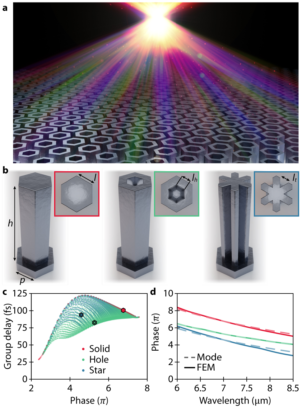
Principle of designing an achromatic metalens.
(a) An achromatic metalens with dispersionless focusing. (b) Schematic of three different metalens elements consisting of Si nanopillars with the height of h = 8 μm and unit cell periodicity p = 2 μm. The displayed shape of elements has varying in-plane geometrical parameters (l, l
h
, l
t
). (c) Phase and group delay for all elements in our library at the center frequency ω0 = 42.62 THz (λ
In previous studies of achromatic metalenses, the phase term has usually been decoupled from the higher-order terms by using the principle of the Pancharatnam–Berry phase [24, 25, 36, 37]. However, as also discussed in Ref. [28, 33], the designed lenses are inherently polarization-dependent, i.e., the incident light is required to have a specific circular polarization in order for the lens to focus. This polarization-sensitive limitation can be overcome by using symmetric pillars – here we utilize structures based on a hexagonal shape to provide the most unimpaired filling of the grid and minimize meta-element variance across the metalenses.
As illustrated in Figure 1(b), three different silicon pillar types, with height h = 8 μm and unit cell periodicity p = 2 μm, but varying in-plane geometrical parameters (
Figure 2(a) shows the meta-element library again (grey dots). Evidently, the library can be described by an upper and lower boundary, modeled as a polynomial interpolation (blue lines). To satisfy Eq. (1), the group delay
We note that the scheme can be used as a general design framework for achromatic metalenses operating at various spectra. Advanced from the previous analytical approach suggested by Shrestha et al. [33], which addressed the problem of negative group delay by engineering
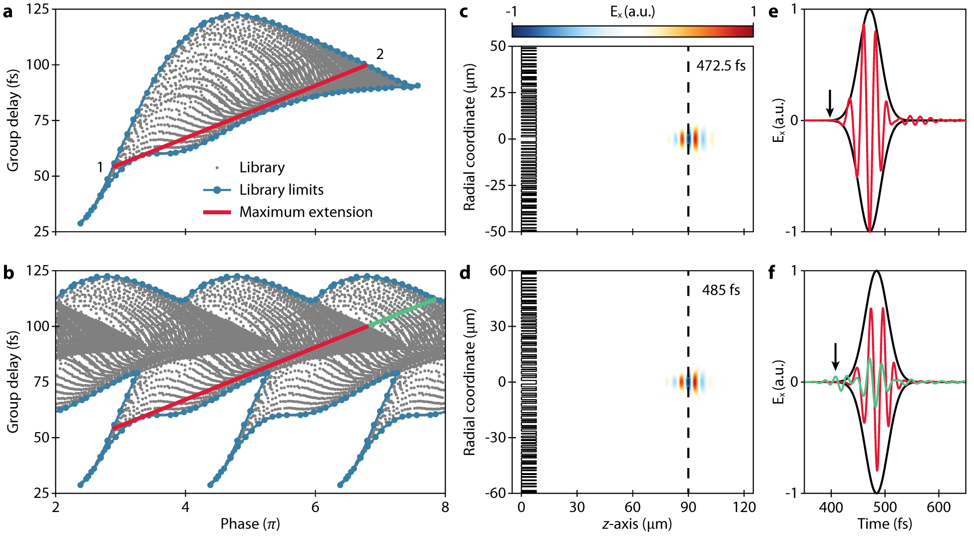
Framework for designing an achromatic metalens.
(a) Phase and group delay for all elements in the presented library, distinctive by the grey dots, with the blue lines defining the upper and lower boundary of the library and the red line displaying the maximal phase range that the library can cover. (b) The same library is duplicated every 2π enabling a longer phase range, i.e., red line plus the additional green line. (c, d) Simulated normalized electric field (x-component) of a 25 fs optical pulse as it is focused at the focal point (f = 90 μm) with the a-type metalens design (NA = 0.49) and b-type metalens design (NA = 0.55), respectively. (e, f) Simulated normalized electric field (x-component) at the focal point as a function of time for the a- and b-type metalens design, respectively. The pulse in (f) is split into the component attributions of the red and green line from (b).
It is noteworthy that the library is repeatable for every 2π, further extending the phase range that the library can cover, warranting a larger numerical aperture (NA, green line in Figure 2(b)). This is an approach utilized in essentially any metalens design. However, it has not been fully investigated how such a library repetition affects the performance of the metasurface for a pulsed input. To analyze this, we compare two metalenses: one designed from the original library shown in Figure 2(a) (called a-type) and the other utilizing the extended library allowing 2π repetition shown in Figure 2(b) (called b-type). The two metalenses are designed to have the same focal length f = 90 μm and library-limited diameters of D = 100 μm (NA = 0.49) and D = 120 μm (NA = 0.55) for the a- and b-type, respectively. For both cases, only “hole” elements are employed, and one “solid” element is used for the center of the lens. This is sensible because the predominant elements in the low group delay region of the library are “hole” elements and a drastic change in element geometry is more likely to cause unexpected inter-element coupling. The exact fitting procedure employed is further described in Supplementary information section S3.
The time-dependent propagation of a 25 fs optical pulse impinging on the a- and b-type lenses are simulated using the three-dimensional finite-difference time-domain (FDTD) method. Figure 2(c) and (d) shows the electric field snapshots of the a- and b-type lens systems taken at t = 472.5 and 485 fs, respectively. Note that it takes a longer time for the b-type lens to focus the pulse because of its larger diameter. Interestingly, the snapshots reveal a slight discrepancy in the wavefront propagation caused by the two different lenses. The b-type lens results in a more elongated pulse compared to the a-type lens at the focal point, but the observable aberration is modest. We attribute this to two reasons: first, the abrupt phase jump in the b-type lens system causes irregularities in the wavefront (Figure S5); second, the meta-elements from the extended part of the library exhibit non-ideal wave transmission behavior due to the excitation of higher-order modes and the non-linear dispersion terms as shown in Figure S6 (see Supplementary information section S4). The latter point becomes more evident by observing the electric field at the focal point in time as shown in Figure 2(e) and (f). The field of the b-type metalens is split into the contributions from the red and green line parts of the lens. The contribution from the red line, which is using the same part of the library as the a-type lens, displays a clear focusing behavior similar to the a-type lens. However, the contribution from the duplicated part of the library (the green line) arrives at the focal point earlier as indicated by the black arrow in Figure 2(f), causing a peculiar distortion of the waveform in the time-domain. The distortion of the waveform further increases as the metalens incorporates more meta-elements from the duplicated part of the library (i.e., increasing the length of the green design line) as shown in Figure S7. We anticipate that the problem of wave packet distortion of achromatic metalenses for pulsed inputs will become an important issue in ultrafast optical systems as the pulse duration reduces to a few optical cycles [45, 46].
To verify the achromatic nature of the designed metalenses, the focal lengths at different wavelengths are determined by analyzing the intensity profiles (point spread functions) along the propagation direction (z-axis) of a continuous wave incident light beam (Figure 3). The a-type lens intensity distribution reveals chromatic aberrations are significantly reduced, over the entire bandwidth, with an observable focal length variation of no consequence (Figure 3(a)). This negligible focal length variation is further exemplified by investigating the point spread function at the target of f = 90 μm, where no defocusing is apparent. In fact, the outstanding suppression of chromatic aberrations suggests that the focal spot would maintain its profile for an appreciable increase of the characterization spectrum. Moreover, it is common to observe significant parasitic focal spots – partly due to an arbitrary design framework – meaning that the metalens is inaccurately focusing the incident light beam [26, 33, 36, 37]; however, such deficiencies are not evident using our methodology. Figure 3(b) complements these observations by displaying the intensity distribution for the b-type metalens, where a slight focal length variation but no parasitic focal spots are observed over the entire bandwidth. A smaller focal spot is observed in this case, attributable to the higher NA of the particular lens.
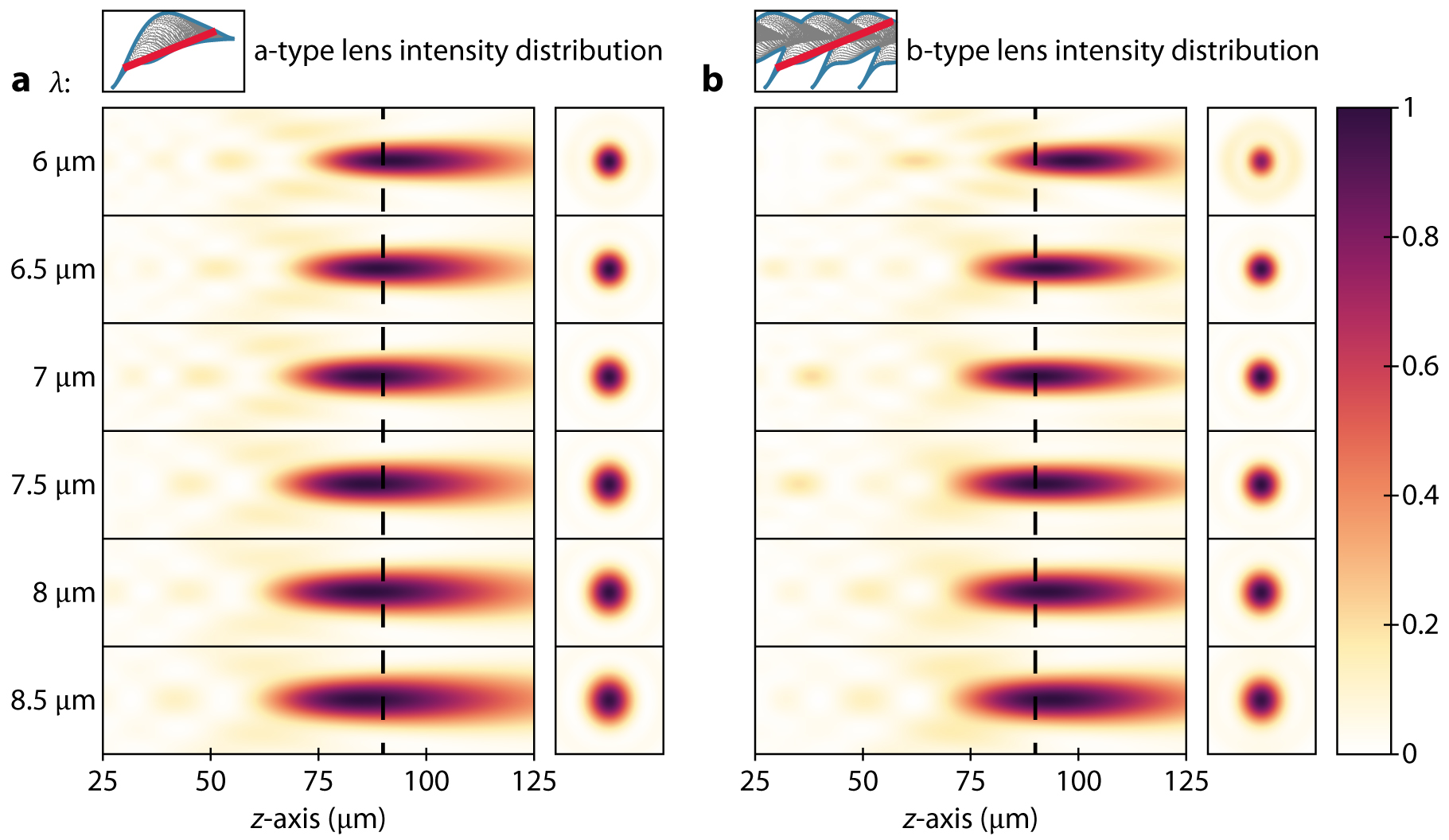
Intensity distributions and focal length shifts of metalenses in the wavelength range λ = 6–8.5 μm.
(a, b) Simulated normalized intensity distributions of the designed a- and b-type metalens, respectively, and their associated point spread functions at the target focal length of f = 90 μm.
The exact focal length, at any given wavelength, corresponds to the z-coordinate possessing the highest intensity value. Figure 4(a) shows the simulated focal lengths of the metalenses and reveals that the foci are not perfectly established at the design focal point with a maximum deviation from the target approaching 10%. However, the variation of focal length, over the entire bandwidth, is insignificant considering that the designed focal point generally lies within the range of the depth of field (DoF), which is defined as the region in which the electric field intensity is higher than 95% of the value at the focal point.
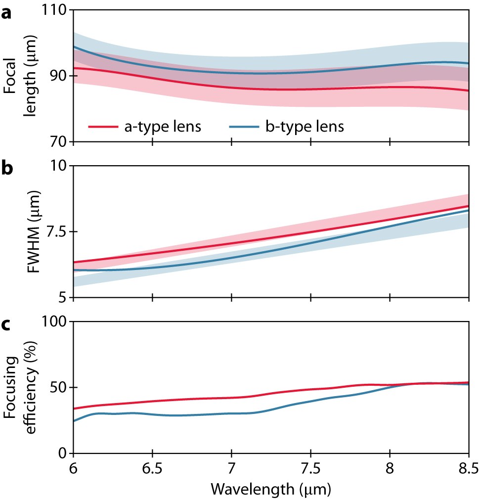
Figures of merit of the metalenses in the wavelength range λ = 6–8.5 μm.
(a) Focal length as a function of wavelength. Shadings indicate the depth of field (DoF) – here defined as the region in which the intensity is higher than 95% of the value at the focal point. (b) Full width at half maximum (FWHM) of the point spread function at the focal spots, where shadings indicate the diffraction limit ranges that correspond to the observed focal length variations in (a). (c) Focusing efficiencies.
Figure 4 summarizes other important figures of merit as well, including the focal spot size and the focusing efficiency. Both lenses display nearly ideal full width at half maximum (FWHM) values close to the theoretical diffraction limit as shown in Figure 4(b). Due to the larger NA of the b-type lens, it slightly outperforms the a-type lens. The shaded areas indicate the ranges of the diffraction limit that correspond to the observed focal spot variations. The focusing efficiency here is defined as the ratio of optical power enclosed in a 3FWHM area of the focal spot to the optical power of the incident beam. The remarkable localization of field power, at the desired focal point, leads to a focusing efficiency of 41% averaged over the entire bandwidth for both lenses with a maximum efficiency above 54% (Figure 4(c)). The variation of the focusing efficiency can be attributed to the transmission amplitude variations among the meta-elements, which may stem from neglecting higher-order modes in our model. Furthermore, the nearest-neighbor effects – i.e., optical response perturbations caused by adjacent meta-elements – will play a role in the slight variations. These effects combined lead to non-negligible unanticipated reflection which limits the focusing efficiencies. Correcting the focusing efficiencies with respect to the metalens transmission yields a normalized focusing efficiency over 80 % and 65% in the whole spectrum for the a- and b-type metalenses, respectively (see Supplementary information section S6). This implies that it is possible to further improve the focusing efficiency by suppressing the reflection loss. To minimize reflection, it is critical to match the wave impedance of the metalens to that of free space, which requires an elaborate design of meta-elements employing full-wave simulations. Nevertheless, we note that, while the efficiencies of the presented metalenses are not fully on par with monochromatic designs [20], [21], [22], they are comparable and even outperform other recent dielectric achromatic metalens demonstrations [23], [24], [25], [26], [27], [28], [29], [30], [31], [32], [33], [34], [35], [36], [37].
Additionally, our design methodology allows for the generation of a broadband focused vortex-beam with polarization-independence. In order to do so, the metasurface should incorporate the phase profile of a metalens (Eq. (1)) and a q-plate together:
Where l is the topological charge and
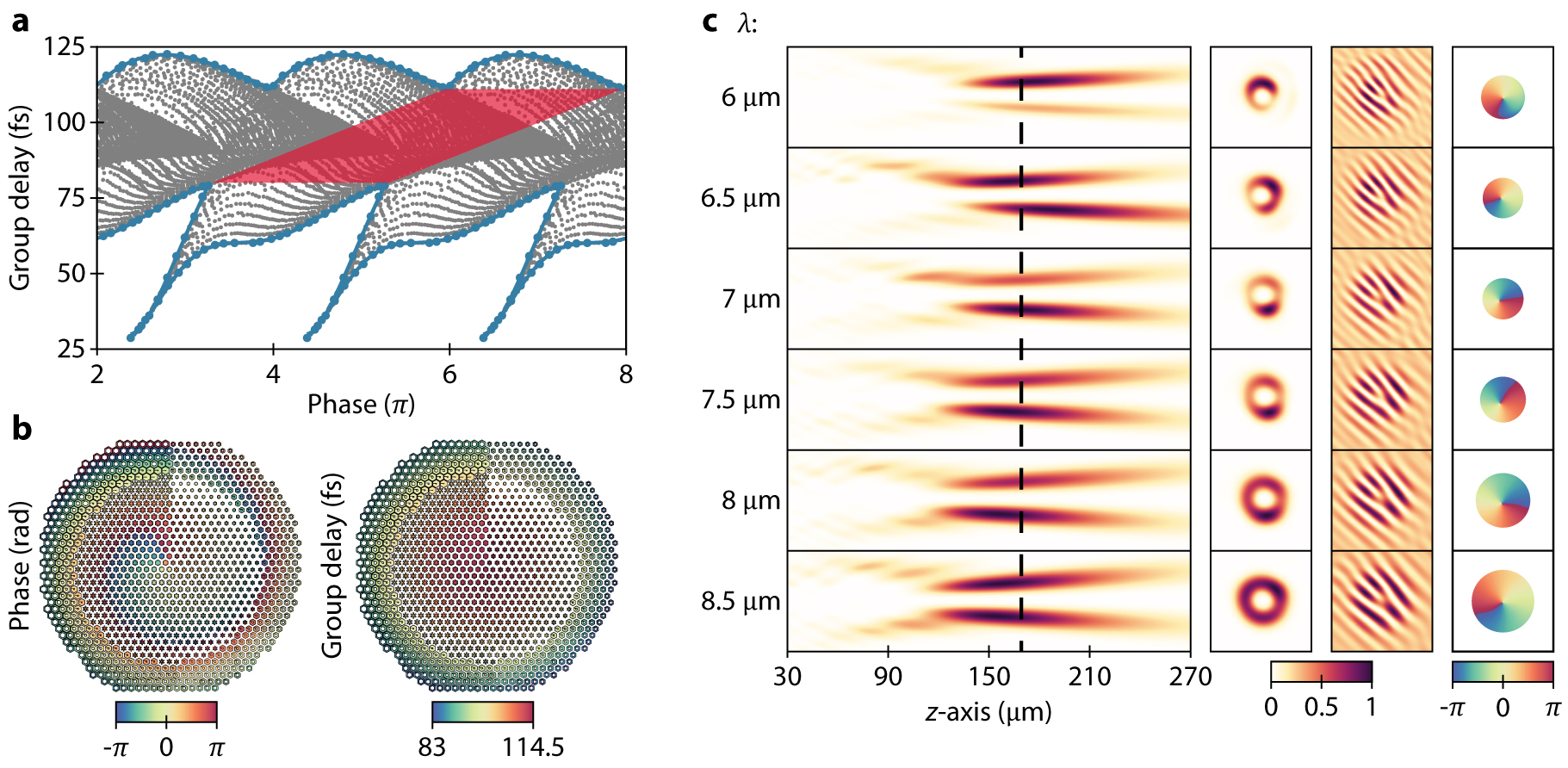
Framework for designing an achromatic metalens generating and focusing a vortex-beam.
(a) Phase and group delay for all elements in the presented library distinctive by the grey dots, with the blue lines defining the upper and lower boundary of the library, and the red shaded area displaying the maximal phase range which the library can cover. (b) A metalens designed with the vortex-beam focusing framework, carrying OAM l = −1. The color overlays indicate the phase (left) and group delay (right) held by each element. (c) Simulated normalized intensity distributions of the designed metalens, its cross-section, interference pattern, and phase at the focal length of f = 165 μm.
The intensity distribution reveals that chromatic aberrations are significantly reduced over the entire bandwidth. However, a noteworthy difference between the desired and the achieved focal length is observed, as the focal point appears at f
3 Conclusions
In summary, we have demonstrated an analytical framework prescribing the exact phase range and appropriate spectral degree of freedom
4 Methods
We performed three-dimensional FEM simulations using a commercial software package (COMSOL Multiphysics 5.4). Periodic boundary conditions are applied on the cross-sectional boundaries of the unit-cell, and the perfectly matched layer (PML) is used above and below the meta-element to truncate the simulation domain. To excite the dielectric meta-element, a plane wave impinges normally on the structure from the bottom.
We performed three-dimensional FDTD simulations using a commercial software package (Lumerical Inc.). The simulations inject a plane wave – in silicon – with normal incidence to the surface. A circular aperture (perfect electric conductor) was implemented between the source and metalens, limiting the area of injection to the exact metalens area. To truncate the air domains surrounding the metalens, PMLs were set as simulation boundaries – all boundaries were placed more than two wavelengths away from everything.
Supporting Information
The following files are available free of charge. Supplementary information (Supplementary information.pdf).
Abbreviations
- MIR
-
mid-infrared
- OAM
-
orbital angular momentum
- FEM
-
finite-element method
- NA
-
numerical aperture
- FDTD
-
finite-difference time-domain
- DoF
-
depth of field
- FWHM
-
full width at half maximum
Funding source: National Research Foundation of Korea
Award Identifier / Grant number: 2016M3D1A1900038
Award Identifier / Grant number: 2017R1E1A1A01074323
Award Identifier / Grant number: 2019K1A3A1A14064929
Award Identifier / Grant number: BK21 FOUR
-
Author contribution: J.T.H. and M.S.J conceived the study. J.T.H. and M.S.J. developed the design framework. J.T.H. performed simulations and developed codes. J.T.H. and M.S.J. wrote the manuscript.
-
Research funding: This work was supported by the National Research Foundation of Korea (NRF) funded by Ministry of Science and ICT (Grants No. 2019K1A3A1A14064929, 2017R1E1A1A01074323, and 2016M3D1A1900038). This work was also supported by the BK21 FOUR Program through the NRF funded by Ministry of Education.
-
Conflict of interest statement: The authors declare no conflicts of interest regarding this article.
References
[1] F. L. Pedrotti and L. S. Pedrotti, Introduction to Optics, Englewood Cliffs, NJ, USA, Prentice-Hall, 1993.Suche in Google Scholar
[2] N. Yu and F. Capasso, “Flat optics with designer metasurfaces,” Nat. Mater., vol. 13, pp. 139–150, 2014, https://doi.org/10.1038/nmat3839.Suche in Google Scholar PubMed
[3] F. Ding, A. Pors, and S. I. Bozhevolnyi, “Gradient metasurfaces: a review of fundamentals and applications,” Rep. Prog. Phys., vol. 81, p. 026401, 2018, https://doi.org/10.1088/1361-6633/aa8732.Suche in Google Scholar PubMed
[4] S. Kim, S. G. Menabde, V. W. Brar, and M. S. Jang, “Functional mid-infrared polaritonics in van der Waals crystals,” Adv. Opt. Mater., vol. 8, p. 1901194, 2020, https://doi.org/10.1002/adom.201901194.Suche in Google Scholar
[5] X. Ni, A. V. Kildishev, and V. M. Shalaev, “Metasurface holograms for visible light,” Nat. Commun., vol. 4, p. 2807, 2013, https://doi.org/10.1038/ncomms3807.Suche in Google Scholar
[6] G. Zheng, H. Mühlenbernd, M. Kenny, G. Li, T. Zentgraf, and S. Zhang, “Metasurface holograms reaching 80% efficiency,” Nat. Nanotechnol., vol. 10, pp. 308–312, 2015, https://doi.org/10.1038/nnano.2015.2.Suche in Google Scholar PubMed
[7] X. Li, L. Chen, Y. Li, et al.., “Multicolor 3D meta-holography by broadband plasmonic modulation,” Sci. Adv., vol. 2, p. e1601102, 2016, https://doi.org/10.1126/sciadv.1601102.Suche in Google Scholar PubMed PubMed Central
[8] A. C. Overvig, S. Shrestha, S. C. Malek, et al.., “Dielectric metasurfaces for complete and independent control of the optical amplitude and phase,” Light Sci. Appl., vol. 8, p. 92, 2019, https://doi.org/10.1038/s41377-019-0201-7.Suche in Google Scholar PubMed PubMed Central
[9] F. Ding, B. Chang, Q. Wei, L. Huang, X. Guan, and S. I. Bozhevolnyi, “Versatile polarization generation and manipulation using dielectric metasurfaces,” Laser Photon. Rev., vol. 14, p. 2000116, 2020, https://doi.org/10.1002/lpor.202000116.Suche in Google Scholar
[10] A. Pors, M. G. Nielsen, and S. I. Bozhevolnyi, “Plasmonic metagratings for simultaneous determination of Stokes parameters,” Optica, vol. 2, pp. 716–723, 2015, https://doi.org/10.1364/optica.2.000716.Suche in Google Scholar
[11] E. Maguid, I. Yulevich, D. Veksler, V. Kleiner, M. L. Brongersma, and E. Hasman, “Photonic spin-controlled multifunctional shared-aperture antenna array,” Science, vol. 352, pp. 1202–1206, 2016, https://doi.org/10.1126/science.aaf3417.Suche in Google Scholar PubMed
[12] F. Ding, A. Pors, Y. Chen, V. A. Zenin, and S. I. Bozhevolnyi, “Beam-size-invariant spectropolarimeters using gap-plasmon metasurfaces,” ACS Photonics, vol. 4, pp. 943–949, 2017, https://doi.org/10.1021/acsphotonics.6b01046.Suche in Google Scholar
[13] N. Yu, F. Aieta, P. Genevet, M. A. Kats, Z. Gaburro, and F. Capasso, “A broadband, background-free quarter-wave plate based on plasmonic metasurfaces,” Nano Lett., vol. 12, pp. 6328–6333, 2012, https://doi.org/10.1021/nl303445u.Suche in Google Scholar PubMed
[14] Y. Yang, W. Wang, P. Moitra, I. I. Kravchenko, D. P. Briggs, and J. Valentine, “Dielectric meta-reflectarray for broadband linear polarization conversion and optical vortex generation,” Nano Lett., vol. 14, pp. 1394–1399, 2014, https://doi.org/10.1021/nl4044482.Suche in Google Scholar PubMed
[15] P. C. Wu, W.-Y. Tsai, W. T. Chen, et al.., “Versatile polarization generation with an aluminum plasmonic metasurface,” Nano Lett., vol. 17, pp. 445–452, 2017, https://doi.org/10.1021/acs.nanolett.6b04446.Suche in Google Scholar PubMed
[16] J. T. Heiden, F. Ding, J. Linnet, Y. Yang, J. Beermann, and S. I. Bozhevolnyi, “Gap‐surface plasmon metasurfaces for broadband circular‐to‐linear polarization conversion and vector vortex beam generation,” Adv. Opt. Mater., vol. 7, p. 1801414, 2019, https://doi.org/10.1002/adom.201801414.Suche in Google Scholar
[17] X. Ni, S. Ishii, A. V. Kildishev, and V. M. Shalaev, “Ultra-thin, planar, Babinet-inverted plasmonic metalenses,” Light Sci. Appl., vol. 2, p. e72, 2013, https://doi.org/10.1038/lsa.2013.28.Suche in Google Scholar
[18] A. Pors, M. G. Nielsen, R. L. Eriksen, and S. I. Bozhevolnyi, “Broadband focusing flat mirrors based on plasmonic gradient metasurfaces,” Nano Lett., vol. 13, pp. 829–834, 2013, https://doi.org/10.1021/nl304761m.Suche in Google Scholar PubMed
[19] A. Arbabi, Y. Horie, A. J. Ball, M. Bagheri, and A. Faraon, “Subwavelength-thick lenses with high numerical apertures and large efficiency based on high-contrast transmitarrays,” Nat. Commun., vol. 6, p. 7069, 2015, https://doi.org/10.1038/ncomms8069.Suche in Google Scholar PubMed
[20] A. Arbabi, Y. Horie, M. Bagheri, and A. Faraon, “Dielectric metasurfaces for complete control of phase and polarization with subwavelength spatial resolution and high transmission,” Nat. Nanotechnol., vol. 10, pp. 937–943, 2015, https://doi.org/10.1038/nnano.2015.186.Suche in Google Scholar PubMed
[21] M. Khorasaninejad, W. T. Chen, R. C. Devlin, J. Oh, A. Y. Zhu, and F. Capasso, “Metalenses at visible wavelengths: diffraction-limited focusing and subwavelength resolution imaging,” Science, vol. 352, pp. 1190–1194, 2016, https://doi.org/10.1126/science.aaf6644.Suche in Google Scholar PubMed
[22] M. S. Carstensen, X. Zhu, O. E. Iyore, N. A. Mortensen, U. Levy, and A. Kristensen, “Holographic resonant laser printing of metasurfaces using plasmonic template,” ACS Photonics, vol. 5, pp. 1665–1670, 2018, https://doi.org/10.1021/acsphotonics.7b01358.Suche in Google Scholar
[23] M. Khorasaninejad, Z. Shi, A. Y. Zhu, et al.., “Achromatic metalens over 60 nm bandwidth in the visible and metalens with reverse chromatic dispersion,” Nano Lett., vol. 17, pp. 1819–1824, 2017, https://doi.org/10.1021/acs.nanolett.6b05137.Suche in Google Scholar PubMed
[24] W. T. Chen, A. Y. Zhu, V. Sanjeev, et al.., “A broadband achromatic metalens for focusing and imaging in the visible,” Nat. Nanotechnol., vol. 13, pp. 220–226, 2018, https://doi.org/10.1038/s41565-017-0034-6.Suche in Google Scholar PubMed
[25] S. Wang, P. C. Wu, V.-C. Su, et al.., “A broadband achromatic metalens in the visible,” Nat. Nanotechnol., vol. 13, pp. 227–232, 2018, https://doi.org/10.1038/s41565-017-0052-4.Suche in Google Scholar PubMed
[26] W. T. Chen, A. Y. Zhu, J. Sisler, Z. Bharwani, and F. Capasso, “A broadband achromatic polarization-insensitive metalens consisting of anisotropic nanostructures,” Nat. Commun., vol. 10, p. 355, 2019, https://doi.org/10.1038/s41467-019-08305-y.Suche in Google Scholar PubMed PubMed Central
[27] R. J. Lin, V.-C. Su, S. Wang, et al.., “Achromatic metalens array for full-colour light-field imaging,” Nat. Nanotechnol., vol. 14, pp. 227–231, 2019, https://doi.org/10.1038/s41565-018-0347-0.Suche in Google Scholar PubMed
[28] Z. B. Fan, H.-Y. Qiu, H.-L. Zhang, et al.., “A broadband achromatic metalens array for integral imaging in the visible,” Light Sci. Appl., vol. 8, p. 67, 2019, https://doi.org/10.1038/s41377-019-0178-2.Suche in Google Scholar PubMed PubMed Central
[29] H. Chung and O. D. Miller, “High-NA achromatic metalenses by inverse design,” Opt Express, vol. 28, pp. 6945–6965, 2020, https://doi.org/10.1364/oe.385440.Suche in Google Scholar
[30] M. Khorasaninejad, F. Aieta, P. Kanhaiya, et al.., “Achromatic metasurface lens at telecommunication wavelengths,” Nano Lett., vol. 15, pp. 5358–5362, 2015, https://doi.org/10.1021/acs.nanolett.5b01727.Suche in Google Scholar PubMed
[31] E. Arbabi, A. Arbabi, S. M. Kamali, Y. Horie, and A. Faraon, “Controlling the sign of chromatic dispersion in diffractive optics with dielectric metasurfaces,” Optica, vol. 4, pp. 625–632, 2017, https://doi.org/10.1364/optica.4.000625.Suche in Google Scholar
[32] S. Wang, P. C. Wu, V.-C. Su, et al.., “Broadband achromatic optical metasurface devices,” Nat. Commun., vol. 8, p. 187, 2017, https://doi.org/10.1038/s41467-017-00166-7.Suche in Google Scholar PubMed PubMed Central
[33] S. Shrestha, A. C. Overvig, M. Lu, A. Stein, and N. Yu, “Broadband achromatic dielectric metalens,” Light Sci. Appl., vol. 7, p. 85, 2018, https://doi.org/10.1038/s41377-018-0078-x.Suche in Google Scholar PubMed PubMed Central
[34] A. Ndao, L. Hsu, J. Ha, J.-H. Park, C. Chang-Hasnain, and B. Kanté, “Octave bandwidth photonic fishnet-achromatic-metalens,” Nat. Commun., vol. 11, p. 3205, 2020, https://doi.org/10.1038/s41467-020-17015-9.Suche in Google Scholar PubMed PubMed Central
[35] Y. Wang, Q. Chen, W. Yang, et al.., “High-efficiency broadband achromatic metalens for near-IR biological imaging window,” Nat. Commun., vol. 12, p. 5560, 2021, https://doi.org/10.1038/s41467-021-25797-9.Suche in Google Scholar PubMed PubMed Central
[36] K. Ou, F. Yu, G. Li, et al.., “Mid-infrared polarization-controlled broadband achromatic metadevice,” Sci. Adv., vol. 6, p. eabc0711, 2020, https://doi.org/10.1126/sciadv.abc0711.Suche in Google Scholar PubMed PubMed Central
[37] K. Ou, F. Yu, G. Li, et al.., “Broadband Achromatic metalens in mid-wavelength infrared,” Laser Photon. Rev., vol. 15, p. 2100020, 2021, https://doi.org/10.1002/lpor.202100020.Suche in Google Scholar
[38] F. Presutti and F. Monticone, “Focusing on bandwidth: achromatic metalens limits,” Optica, vol. 7, 2020, pp. 624–631, https://doi.org/10.1364/optica.389404.Suche in Google Scholar
[39] J. Engelberg and U. Levy, “Achromatic flat lens performance limits,” Optica, vol. 8, pp. 834–845, 2021, https://doi.org/10.1364/optica.422843.Suche in Google Scholar
[40] F. Aieta, M. A. Kats, P. Genevet, and F. Capasso, “Multiwavelength achromatic metasurfaces by dispersive phase compensation,” Science, vol. 347, pp. 1342–1345, 2015, https://doi.org/10.1126/science.aaa2494.Suche in Google Scholar PubMed
[41] J. Wang, J.-Y. Yang, I. M. Fazal, et al.., “Terabit free-space data transmission employing orbital angular momentum multiplexing,” Nat. Photonics, vol. 6, pp. 488–496, 2012, https://doi.org/10.1038/nphoton.2012.138.Suche in Google Scholar
[42] J. Yang, I. Ghimire, P. C. Wu, et al.., “Photonic crystal fiber metalens,” Nanophotonics, vol. 8, pp. 443–449, 2019, https://doi.org/10.1515/nanoph-2018-0204.Suche in Google Scholar
[43] Z. Li, P. Lin, Y.-W. Huang, et al.., “Meta-optics achieves RGB-achromatic focusing for virtual reality,” Sci. Adv., vol. 7, p. eabe4458, 2021, https://doi.org/10.1126/sciadv.abe4458.Suche in Google Scholar PubMed PubMed Central
[44] A. Tittl, A. Leitis, M. Liu, et al.., “Imaging-based molecular barcoding with pixelated dielectric metasurfaces,” Science, vol. 360, pp. 1105–1109, 2018, https://doi.org/10.1126/science.aas9768.Suche in Google Scholar PubMed
[45] C. Huang, C. Zhang, S. Xiao, et al.., “Ultrafast control of vortex microlasers,” Science, vol. 367, pp. 1018–1021, 2020, https://doi.org/10.1126/science.aba4597.Suche in Google Scholar PubMed
[46] P. Täschler, M. Bertrand, B. Schneider, et al.., “Femtosecond pulses from a mid-infrared quantum cascade laser,” Nat. Photonics, vol. 15, pp. 921–926, 2021.10.1038/s41566-021-00894-9Suche in Google Scholar PubMed PubMed Central
[47] E. Karimi, S. A. Schulz, I. De Leon, H. Qassim, J. Upham, and R. W. Boyd, “Generating optical orbital angular momentum at visible wavelengths using a plasmonic metasurface,” Light Sci. Appl., vol. 3, p. e167, 2014, https://doi.org/10.1038/lsa.2014.48.Suche in Google Scholar
[48] M. Pu, X. Li, X. Ma, et al.., “Catenary optics for achromatic generation of perfect optical angular momentum,” Sci. Adv., vol. 1, p. e1500396, 2015, https://doi.org/10.1126/sciadv.1500396.Suche in Google Scholar PubMed PubMed Central
[49] F. Ding, Y. Chen, and S. I. Bozhevolnyi, “Focused vortex-beam generation using gap-surface plasmon metasurfaces,” Nanophotonics, vol. 9, pp. 371–378, 2019.10.1515/nanoph-2019-0235Suche in Google Scholar
Supplementary Material
The online version of this article offers supplementary material (https://doi.org/10.1515/nanoph-2021-0638).
© 2021 Jacob T. Heiden and Min Seok Jang, published by De Gruyter, Berlin/Boston
This work is licensed under the Creative Commons Attribution 4.0 International License.
Artikel in diesem Heft
- Frontmatter
- Reviews
- A review of terahertz phase modulation from free space to guided wave integrated devices
- Intelligent on-demand design of phononic metamaterials
- Light activation of 3D-printed structures: from millimeter to sub-micrometer scale
- Research Articles
- Unveiling radial breathing mode in a particle-on-mirror plasmonic nanocavity
- Controlling asymmetric transmission phase in planar chiral metasurfaces
- Rayleigh anomaly-enabled mode hybridization in gold nanohole arrays by scalable colloidal lithography for highly-sensitive biosensing
- Enhanced terahertz detection of multigate graphene nanostructures
- The anisotropic broadband surface plasmon polariton and hot carrier properties of borophene monolayer
- Probing higher order optical modes in all-dielectric nanodisk, -square, and -triangle by aperture type scanning near-field optical microscopy
- Cascaded microsphere-coupled surface-enhanced Raman spectroscopy (CMS-SERS) for ultrasensitive trace-detection
- Morphology adjustable microlens array fabricated by single spatially modulated femtosecond pulse
- Design framework for polarization-insensitive multifunctional achromatic metalenses
- Electro-optically modulated lossy-mode resonance
- Double Rabi splitting in methylene blue dye-Ag nanocavity
- Broadband high-efficiency near-infrared graphene phase modulators enabled by metal–nanoribbon integrated hybrid plasmonic waveguides