Dielectric permittivity extraction of MoS2 nanoribbons using THz nanoscopy
-
Henrik B. Lassen


Abstract
The nanoscale optical properties of high-quality MoS2 nanoribbons are investigated using THz nanoscopy based on a scattering-type scanning probe. The nanoribbons comprise a multilayer core, surrounded by monolayer edges. A featureless complex permittivity spectrum covering the range 0.6–1.6 THz is extracted from experimental time-domain measurements through a minimization procedure, adopting an extended finite-dipole model of the probe–sample interaction. Real-space mapping of the nanoribbon reveals variations in the local permittivity down to the instrument-limited resolution, on the order of 30 nm. Clustering analysis statistically identifies regions of lower apparent permittivity that we attribute to a high curvature at the edges of the nanoribbon causing an increase in local material strain or cross-talk in the measured signal with topography-induced measurement artifacts. The core of the nanoribbon contains two regions that follow tightly distributed, but slightly shifted Gaussian statistics in complex permittivity space, with the real part mean of both distributions lying around 5.4 and compatible with literature values of the static permittivity of thin-film MoS2 reported previously. Our results show that the nanoribbons exhibit a modest degree of dielectric variation at the nanoscale that could be explained by heterogeneous doping or variations in the local defect density. We believe that our approach could be useful for the direct real-space measurement of dielectric disorder in other low-dimensional semiconducting material systems.
1 Introduction
The dielectric permittivity of a material is a measure of its response to an electric field and is a frequency-dependent complex quantity. It is, therefore, a fundamental property of the material, governed by a specific chemical and structural composition, required in the design of semiconductor electronics. Recently, dielectric disorder in nanoscale systems – fluctuations in local complex permittivity on optical length scales – has been identified to contribute strongly to variations in the optoelectronic performance and transport properties of two-dimensional (2D) materials [1]. Transition-metal dichalcogenides (TMDs) are a family of 2D layered crystals, a subset of which are semiconducting and well-known to possess distinct properties in their mono- and few-layer form, namely a transition from indirect to direct electronic bandgap, compared to bulk. This behavior marks out several TMDs in particular, including MoS2, WSe2, MoSe2, and more, as attractive materials for photonic and optoelectronic device applications, such as light-emitting diodes, photodetectors [2], and photovoltaics [3], among others, due to an increased efficiency of light–matter interaction driving a stronger photoluminescence and greater light absorption. A further lowering of the physical dimensions can dramatically influence the intrinsic material properties [4], [5], [6], boosting photoresponsivity and nonlinear effects [7], [8]. The potential of TMD-based nanostructures, including MoS2 nanoribbons, has pushed the development of numerous TMD synthesis methods forward and emphasized the importance of dedicated characterization of TMD properties [9], [10], [11], [12], [13].
Angle-dependent Raman [14], [15] and photoluminescence spectroscopies [16], [17] have been widely applied in the study of layered materials, providing rich information on crystallographic structure including anisotropy, vibrational modes, strain, band structure, and defects; neither technique, however, directly captures the dielectric function and both are typically restricted in their ability to resolve features in materials or heterogeneities in optical properties smaller than is allowed by the diffraction-limited focusing of visible light (typically several hundreds of nanometers at best). Ellipsometry [18] and impedance spectroscopy [19], on the other hand, can directly record the frequency-dependent dielectric permittivity (albeit in very distinct frequency regions, either in the visible/near-infrared or radio frequency range), but are again subject to either the diffraction limit of optical systems or determine only an average macroscopic material response. Similarly, time-domain methods in the infrared and low-frequency terahertz (THz) region of the electromagnetic spectrum, notably THz time-domain spectroscopy (TDS) [20], have proven effective for material characterization because THz radiation, in particular, is commensurate with the energy scale of free carriers in materials leading to a strong interaction. THz-TDS has been widely applied to semiconducting and metallic thin films, including graphene, to investigate complex permittivity and conductivity, without contacts [21], [22]. However, the challenge is again the spatial resolution, which is now limited to several tens or even hundreds of micrometers because of the low frequency (typically 0.3–3 THz) of the probing radiation.
Scanning probe microscopy (SPM) techniques, such as atomic force microscopy (AFM) using sharpened (conductive) tips with an apex radius on the order of several tens of nanometers, can be used to explore material properties with significantly enhanced spatial resolution and are, therefore, suitable for studying nanostructured and heterogeneous materials locally. Electrostatic force microscopy (EFM) – an AFM-based technique exploiting the change in capacitance between a voltage-biased probe and the sample surface to infer dielectric properties – is one example that has been applied to thin-film TMDs for recovery of the local electrostatic dielectric constant at (or very close to) DC [23], [24] but importantly does not provide information of dielectric relaxation behavior in even a limited frequency range. Scattering-type scanning near-field optical microscopy (s-SNOM) [25], [26], essentially a modified AFM with an external light source, equipped with infrared or THz illumination has become a powerful technique for nanoscale imaging and spectroscopy in a technologically relevant frequency range, combining the benefits of both sensitivity to free-carrier absorption of far-field THz-TDS, with the nanoscale resolution of other surface probes. The spatial resolution of s-SNOM is essentially agnostic to the wavelength of the illuminating light source [27] and is rather defined by the radius of the scanning probe (or tip) at its apex. THz-SNOM, therefore, probes a similar volume in real-space compared to SNOM illuminated with visible light. Significantly, however, the mismatch between the free-space wave-vector and the (in-plane) momenta of tip-scattered light at THz frequencies can reach 103, meaning THz-SNOM probes deeply into the near-field regime. When the light source is a broadband THz pulse covering a wide frequency range, THz-enabled SNOM becomes a potent tool for nanoscopy of advanced materials. The challenge of SPM methods is often to accurately represent the tip–sample interaction. Quantitative extraction of material properties from experimental near-field scattering data in s-SNOM is often a formidable task, but several attempts in the recent literature have successfully applied an underlying model of the physical tip–sample system that can be inverted to relate fundamental parameters to measurable quantities [28], [29], [30], [31], [32], without needing to make model assumptions about the dielectric function, and in the case of nanoscopy its spectral dependence. The inversion can be performed with an analytic approximation [29] or using an iterative numerical minimization algorithm [33], with both demonstrated to yield robust and reliable output. Here, we use ultrafast THz pulses with a useful bandwidth spanning 0.6–1.6 THz for nanoscopy in an s-SNOM setup to interrogate MoS2 nanoribbons and recover their complex dielectric response using a numerical minimization procedure based on an extended finite-dipole model for a layered material system [34], [35], [36]. Subsequent nanoscale THz imaging of the nanoribbon and a clustering analysis of the spatially dependent dielectric data is used to identify regions strongly influenced by edge effects where high surface curvature could indicate an impact from local strain or cross-talk from topographic artifacts, together with regions in the core of the nanoribbon where we observe two clearly distinguishable areas defined by tightly distributed Gaussian statistics that we believe capture directly nanoscale variations in the materials dielectric response.
2 Materials and methods
2.1 Nanoribbon growth
The MoS2 nanoribbons were grown on a c-cut sapphire substrate. Synthesis was a two-step process in which ultra-thin oxide films of MoO3-x (with many oxygen vacancies) grown by pulsed laser deposition were sulfurized at the second step in the presence of a NaF layer, the details of the process can be found in our previous works [8], [37]. The technique is similar to that described by Li et al. in Ref. [5] and shares many similar ideas on liquid phase creation and vapor–liquid–solid phase reaction. Briefly, the growth process evolves via the formation of the Na–Mo–O liquid phase, which mediates the formation of MoS2 multilayer nanoribbons in a sulfur-rich environment [5], [8], [37]. The nanoribbons crystallize predominantly in the 2H stacking orientation [8]. Due to strong in-plane covalent bonding and weak out-of-plane van der Waals (vdW) interactions, layered 2D materials possess a strongly anisotropic dielectric tensor [38], with distinct in-plane and out-of-plane components. Figure 1a shows a secondary-electron scanning electron microscope (SEM) image of a typical MoS2 nanoribbon on sapphire with a length of 10 μm and a width of less than 0.5 μm, resulting in a length-to-width ratio of nearly 20. Isolated 2D and 3D crystallites of MoS2 can also been seen in the SEM image. A typical Raman spectrum of such samples taken using a laser with a wavelength of 532 nm is shown in Figure 1b. The spectrum shows two major characteristic Raman peaks of MoS2 arising from the in-plane
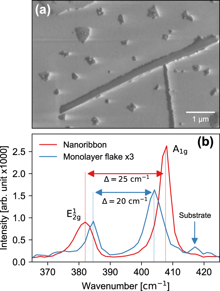
Characteristic nanoribbon properties. (a) SEM image of a characteristic MoS2 nanoribbon surrounded by triangular 2D and 3D crystallites of MoS2 and (b) Raman spectrum obtained from a region of the MoS2 nanoribbon (blue) and on a 2D MoS2 crystal (orange). The signal from monolayer MoS2 has been multiplied by a factor of 3 for better representation.
The exact dimensions of the MoS2 nanoribbon used in this study can be inferred from the AFM images in Figure 2a and b, showing an overview and zoom-in (corresponding to the area indicated by the dotted red box in Figure 2a). The thickness of the nanoribbon (as confirmed by our AFM measurements, e.g., Figure 2a) varies between approximately 10 nm and 15 nm, correspondingly the multilayer core of the nanoribbon consists of >15 layers suggesting the properties approach that of the bulk crystal. Notably, monolayer edges of the MoS2 nanoribbon that can be observed in the SEM imaging are not visible with AFM. It should be noted that the SEM and AFM were not performed on the same nanoribbon. The reason for discrepancies between the SEM and AFM images can be twofold: (i) these edges are not pronounced in the selected nanostructure or (ii) a limitation of the instrument: compared to SEM, AFM has a poor depth of field, limiting its ability to resolve features with large height differences. The abrupt change in thickness between the multilayer nanoribbon (15L) and the adjacent monolayer (1L) could make the monolayer edge undetectable by AFM.
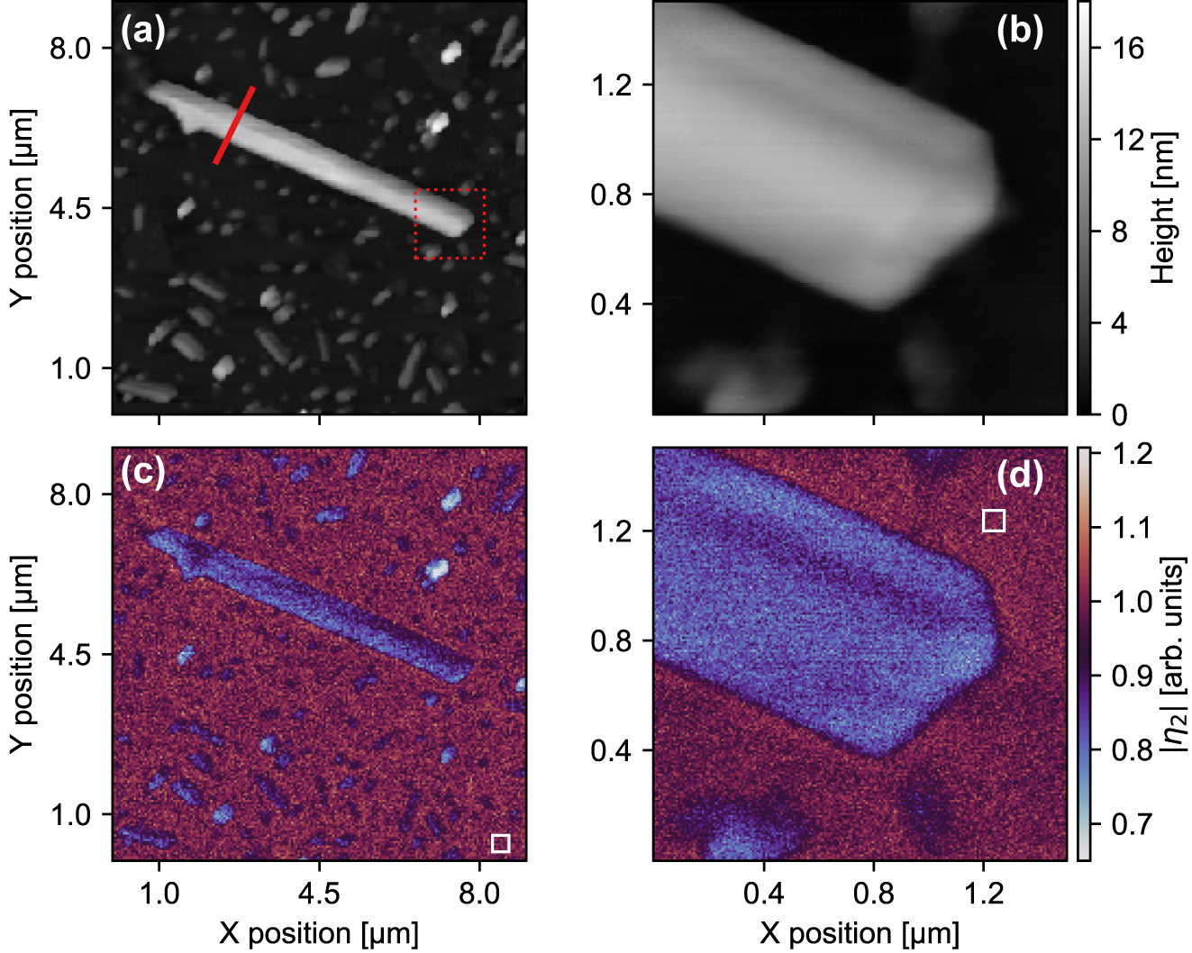
Topography and scattering contrast maps. (a) AFM images of the selected MoS2 nanoribbon and (b) a zoom-in scan of one end of the nanoribbon as indicated by the red dotted square in (a). The red line in (a) indicates the position of the spectroscopic line scan (THz nanoscopy). The corresponding white-light mode imaging maps, (c) overview and (d) zoom-in, of the near-field contrast (second-order demodulated scattered signal). The white squares in (c) and (d) indicate the areas used to generate a mean substrate response for normalization.
2.2 Near-field imaging and nanoscopy
The near-field microscope used is a commercial instrument (Attocube THz-NeaSCOPE) equipped with an integrated THz time-domain spectroscopy module (Attocube/Menlo Systems TeraSmart). THz pulses with a useful bandwidth covering the spectral range 0.6–1.6 THz are generated and coherently detected by a photoconductive antenna pair. A conductive AFM tip (with a shank length of 80 μm and typical average tip radius of <40 nm, Rocky Mountain Nanotechnology, 25PtIr200B-H), operated in noncontact tapping mode (at a nominal frequency of 80 kHz), acts as a nanofocusing surface probe, allowing for simultaneous capture of sample topography together with measurements of the scattered near-field signal in a single scan of the sample. Measurements are performed in a nitrogen-rich environment to minimize the presence of water-vapor absorption lines in the detected THz spectra. Background removal is accomplished by demodulation of the scattered field to recover the near-field signal that is most pure in higher overtones of the tapping frequency (typically orders m = 2–4 are used for data retrieval due to diminishing signal-to-noise ratio affecting data quality at orders above 4) [25]. The scattered THz waveform is detected in the time domain in two distinct modes of detection that are common to other THz-SNOM systems. Firstly, white-light (WL) detection offers rapid imaging of the surface by resolving the electric field at the principal peak of the waveform (this corresponds to a spectrally integrated near-field response [41]). In this case, the WL signal,
2.3 Modeling and inversion of the scattering problem
The scattering of a low-frequency electric field by the combined tip–sample system can be described by several self-consistent, quasi-electrostatic models of the problem [25], [31], [35], together with extensions to allow for layered structures, including thin films on a bulk substrate [30], [34], [36], based on a transfer matrix formalism [47]. The finite-dipole model (FDM) [35], and its extensions for layered structures [34], [36], approximates the probe as prolate spheroid. The scattered field is determined by
where f 0,1 represent geometric functions describing the characteristics of the tip (see the Supplementary Information and references therein for details) and β is the complex near-field reflection coefficient that depends on frequency, ω and the in-plane momentum, q of the electric near-field. Importantly, β carries information about the material properties of the sample, including the dielectric permittivity, which in its simplest form is written as β = (ϵ − 1)/(ϵ + 1) (see Supplementary Information for details). Evidently then the process of extracting the material properties follows from an inversion of the scattering problem. This is made more complex by the fact that the height of the tip above the sample surface is not fixed, in order to remove background and isolate the scattered near-field the tip oscillates. Demodulation involves a Fourier decomposition into a series of harmonic orders that describe the overall scattering during a full oscillation cycle. We thus use an algorithmic approach, similar to Refs. [28], [33], where a numerical routine aims to minimize the deviation between measured data and a corresponding scattered signal calculated from the dielectric function using the layer-extended FDM model (see Supplementary Information for further details of the inversion algorithm).
3 Results and discussion
We first show WL imaging of a selected nanoribbon in Figure 2c (overview: 9 × 9 μm at 36 nm per pixel) and Figure 2d (zoom-in: 2 × 2 μm at 10 nm per pixel). Here, we choose to present the second-order demodulated scattered near-field contrast,
Next we perform THz nanoscopy along a specific line, as indicated on Figure 2a. The full scattered THz waveform is captured in the time domain, with a spatial step-size of approximately 10 nm, starting and ending on the substrate and traversing the complete short axis of the nanoribbon. As before when WL imaging, the captured signal is demodulated and normalized to a reference comprising an average response of the substrate to obtain a relative contrast for a given harmonic order (see Supplementary Information for details regarding the normalization procedure). The hyperspectral frequency-position data are spatially averaged over the central region of the nanoribbon where we observe little to no dependence in the contrast as a function of position. The resulting complex Fourier spectrum, and its corresponding standard deviation, for orders two and three is reported in Figure 3a and b, respectively. Both the real and imaginary parts of the contrast exhibit a rather featureless spectrum within the finite bandwidth limits of our probe. The strength of the contrast for the higher demodulation order is marginally greater, but this is accompanied by an increase in the standard deviation due to the corresponding reduced signal-to-noise ratio. The imaginary part is small and appears to be a near-constant value just above zero.
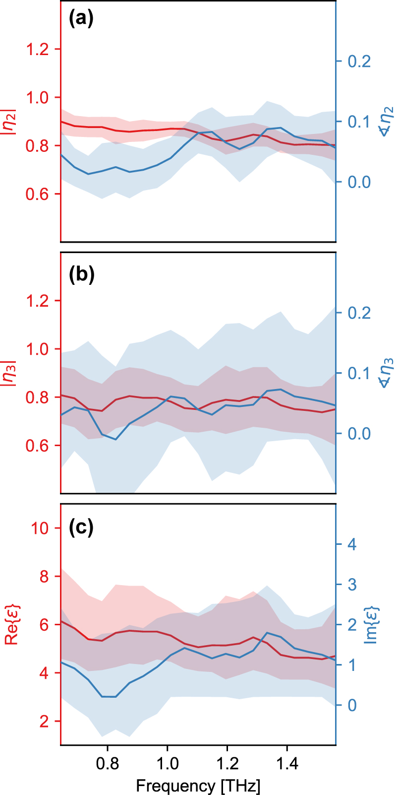
Spectrally resolved THz nanoscopy; (a) second-order contrast and (b) third-order contrast. The solid lines indicate the mean response of 50 adjacent scans at the center of the nanoribbon and the filled area indicates the corresponding standard deviations. (c) Extracted effective complex permittivity spectrum (see Supplementary Information for details of the algorithmic minimization procedure).
To extract the effective complex permittivity from the spectrally dependent scattering contrast, we utilize a numerical minimization procedure to invert the FDM (see the Supplementary Information for details of the algorithm used). Due to the uniaxial anisotropy of the c-cut sapphire substrate, its static effective permittivity was modeled by taking the geometric mean of the in-plane and out-of-plane components,
The featureless spectrum, confirmed by our line-scan measurements using detection of the full scattered THz waveform (TDS-mode) to recover amplitude and phase information, allows us to further analyze the WL imaging – where detection recovers a weighted spectrally integrated electric near-field response – in order to investigate nanoscale variations in the effective permittivity. Using the same inversion procedure as introduced above, but this time applied to the WL data (in Figure 2c and d), we show the extracted real (a, b) and imaginary parts (c, d) of the effective complex permittivity in Figure 4a–d for the overview (a, c) and zoom-in (b, d), respectively. Throughout the inversion, we assume a constant value for the phase of the scattered field taken to be the frequency-resolved average from TDS measurements (see the Supplementary Information for details). While this assumption is imperfect, due to the nature of the WL detection being a mix of contrast due to changes in amplitude and phase, we confirm at several spatial locations across the nanoribbon that this approximation is only a small correction to the full response and variations in the measured contrast, leading to a spatial distribution of extracted permittivities, is dominated by contributions from changes in amplitude (see Figure S1). In contrast to recording the full waveform at each spatial pixel, WL detection is relatively fast. Thus, we believe this approach allows us to rapidly determine nanoscale regions within the entire nanoribbon with distinct distributions of the permittivity that would otherwise be obscured using far-field optical probes that at best could perform a spatially averaged response over a small ensemble of nanoribbons or not captured with single-point THz nanoscopy.

Spatially resolved maps of the real (a, b) and imaginary (c, d) parts of the complex permittivity, extracted from WL imaging of the selected MoS2 nanoribbon, overview (a, c) and zoom-in (b, d).
We perform a clustering analysis of the real-space data in order to identify heterogeneities in the effective permittivity at the nanoscale. In Figure 5a, we show a phase-space representation of the output of a Bayesian Gaussian mixture model that identifies four distinct clusters in the complex plane. In Figure 5b and c, these clusters are projected onto the real and imaginary axis and the resulting distributions are fitted with a Gaussian function, respectively. The horizontal and vertical black dotted lines represent the mean values of the real and imaginary parts, as determined from the THz nanoscopy data (Figure 3c). The clusters (indexed 0–3, with −1 being the substrate) are then mapped back onto the real-space image of the nanoribbon (Figure 5d). A narrow band is evident around the edges of the nanoribbon that corresponds to a broadly distributed Gaussian with a center-of-mass significantly shifted from the spectrally averaged mean determined by THz-SNOM (TDS-mode). The spatial distribution of this cluster, localized to the edges of the nanoribbon, agrees well with regions where we identify a high degree of local surface curvature (inferred from the second-derivative of the AFM topography, see Figure S6). The curvature of TMD films determined in this way has previously been connected with areas of increased local strain [40]. Tensile and compressive strain can influence the dielectric properties of materials. A compressive strain less than 10 % in monolayer MoS2 has been predicted by calculations to result in a lowered static permittivity [54]; typically, the reduction is on the order of several percent, which cannot fully account for the shift away from the mean observed for this edge cluster. We, therefore, suggest that other influences, including artifacts of the measurement from the sample topography and not from the material properties, convolute the data in this region. The second cluster (with index 1) is larger but shows a similarly shifted distribution in the real-part of the permittivity, well separated from the two final clusters (index 2, 3) that comprise the spatial core of the nanoribbon and show the tightest distribution around the mean based on the nanoscopy data. Importantly, these core clusters of the nanoribbon are distinguishable by their permittivity distributions in the complex plane. We propose that this could arise due to subtle differences in their nanoscale material properties, including variations in local carrier concentration or the spatially integrated density of point defects.
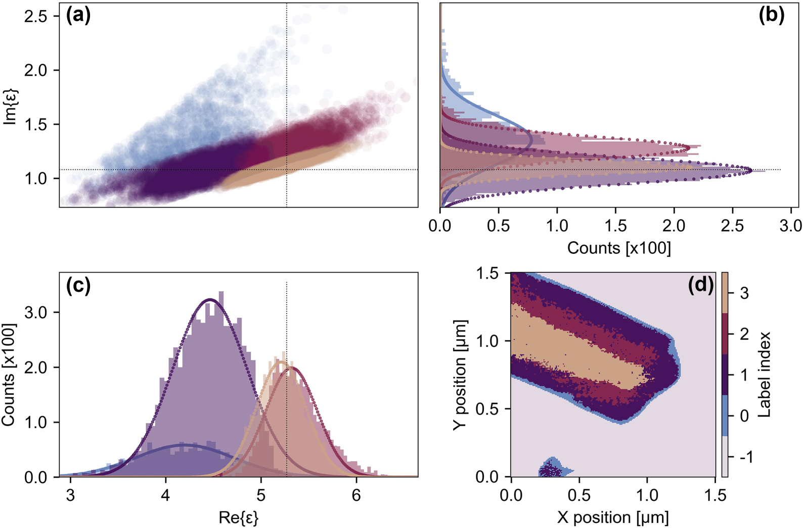
Clustering analysis of the spatially resolved permittivity data. (a) Four distinct clusters in the complex plane. Projections of the four dominant cluster distributions onto the imaginary (b) and real (c) axis. (d) Mapping of the clusters back to real-space to identify variations in the nanoscale permittivity associated with local changes in material properties.
Finally, we note that although the dependence of the extracted effective complex permittivity is essentially independent of the MoS2 nanoribbon thickness (see Figure S7), a transition from a lower to a higher real-part permittivity appears to occur around 8–9 nm (corresponding to approximately 13 atomic layers). Recent studies have shown similar tendencies in the increase of the static permittivity with increasing thickness of MoS2 [23]. An increased surface-to-volume ratio and reduced dimensionality of materials can be associated with an reduction in both the dielectric permittivity and the scattering time of mobile charge carriers in semiconductors and metals, due to the breaking of polarizable bonds and enhanced scattering – surface effects modifying the optical and electrical properties of materials [55]. This could indicate an evolution of the optical properties from single- and few-layer characteristics to a bulk-like behavior. However, we again note that the thinner regions are proximal to the edges of the nanoribbon and, therefore, may be more strongly dominated by edge effects, as discussed above and only weakly dependent on dimensionality.
4 Conclusions
We have quantitatively investigated the nanoscale optical properties of MoS2 nanoribbons using THz-SNOM. Initial WL imaging of an isolated nanoribbon, together with satellite crystallites, revealed a clear spatially resolved contrast in the scattered electric near-fields. THz nanoscopy along a cross section of the nanoribbon allowed us to extract the effective complex permittivity that showed a featureless spectrum within our probe bandwidth, well below the lowest frequency resonances of structural phonon modes in the material, indicating a low carrier concentration consistent with the approximately frequency independent behavior of the complex permittivity of a Drude conductor with a low scattering time. By exploiting the phase information from the line scan measurements, where full scattered THz waveforms are detected in the time domain, we are able to extract spatially resolved maps of the complex permittivity of the nanoribbon from WL imaging data, with only a small error due to the rapid detection method being sensitive only to changes in the peak of the scattered THz waveform. The permittivity images reveal significant nanoscale variations in the optical properties of the nanoribbon (and its crystallites). A clustering analysis allows us to resolve four dominant distributions that are separable in the complex plane and map them back into real-space. This allows us to propose mechanisms, such as local strain gradients proximal to the nanoribbon edges or distributions in the spatially averaged density of point defects that could be driving changes to the permittivity over such length scales, and importantly move toward being able to unambiguously distinguish heterogeneities in nanoscale material properties from measurement artifacts, such as topographic effects, known to challenge interpretation of scanning probe techniques, including THz-SNOM. With very few methodologies available for either the direct quantification or indirect evaluation of the complex optical and electrical properties of materials at the nanoscale and the importance of understanding dielectric behavior, including disorder, for the development of opto- and nanoelectronic devices based on layered materials, we believe this approach will be useful for studying many other semiconducting nanomaterial systems in the future.
Funding source: Danmarks Frie Forskningsfond
Award Identifier / Grant number: 8049- 00095B
Award Identifier / Grant number: 9064-00072B
-
Research funding: SC and EJRK acknowledge financial support from Independent Research Fund Denmark Sapere Aude grants (project number 8049-00095B and project number 9064-00072B).
-
Author contributions: SC, PUJ, and EJRK conceived the idea. HBL, PUJ, and EJRK planned and designed the experiments. The sample, along with the SEM image and Raman spectrum, were provided by DIM, GG, and SC. HBL performed the experiments. HBL performed the data analysis with contributions from WVC, PUJ, and EJRK. WVC performed the statistical cluster analysis. HBL wrote the manuscript with contributions from WVC and EJRK. Edits were provided by all authors. PUJ and EJRK supervised the entire project. All authors have accepted responsibility for the entire content of this manuscript and consented to its submission to the journal, reviewed all the results, and approved the final version of the manuscript.
-
Conflict of interest: Authors state no conflicts of interest.
-
Data availability: The datasets generated during and/or analyzed during the current study are available from the corresponding author on reasonable request.
References
[1] A. Raja, et al.., “Dielectric disorder in two-dimensional materials,” Nat. Nanotechnol., vol. 14, no. 9, pp. 832–837, 2019. https://doi.org/10.1038/s41565-019-0520-0.Suche in Google Scholar PubMed
[2] A. Varghese, et al.., “Near-direct bandgap WSe2/ReS2 type-II pn heterojunction for enhanced ultrafast photodetection and high-performance photovoltaics,” Nano Lett., vol. 20, no. 3, pp. 1707–1717, 2020. https://doi.org/10.1021/acs.nanolett.9b04879.Suche in Google Scholar PubMed
[3] M. M. Furchi, A. Pospischil, F. Libisch, J. Burgdö, and T. Mueller, “Photovoltaic effect in an electrically tunable Van der Waals heterojunction,” Nano Lett., vol. 14, no. 8, pp. 4785–4791, 2014. https://doi.org/10.1021/nl501962c.Suche in Google Scholar PubMed PubMed Central
[4] T. Hu, J. Zhou, J. Dong, and Y. Kawazoe, “Electronic and magnetic properties of armchair MoS2 nanoribbons under both external strain and electric field, studied by first principles calculations,” J. Appl. Phys., vol. 116, no. 6, p. 064301, 2014. https://doi.org/10.1063/1.4891997.Suche in Google Scholar
[5] S. Li, et al.., “Vapour–liquid–solid growth of monolayer MoS2 nanoribbons,” Nat. Mater., vol. 17, no. 6, pp. 535–542, 2018. https://doi.org/10.1038/s41563-018-0055-z.Suche in Google Scholar PubMed
[6] Y. Li, et al.., “Large-scale fabrication of MoS2 ribbons and their light-induced electronic/thermal properties: dichotomies in the structural and defect engineering,” Adv. Funct. Mater., vol. 28, no. 13, p. 1704863, 2018. https://doi.org/10.1002/adfm.201704863.Suche in Google Scholar
[7] T. Chowdhury, et al.., “Substrate-directed synthesis of MoS2 nanocrystals with tunable dimensionality and optical properties,” Nat. Nanotechnol., vol. 15, no. 1, pp. 29–34, 2020. https://doi.org/10.1038/s41565-019-0571-2.Suche in Google Scholar PubMed
[8] G. Ghimire, et al.., “Molybdenum disulfide nanoribbons with enhanced edge nonlinear response and photoresponsivity,” Adv. Mater., vol. 35, no. 31, p. 2302469, 2023. https://doi.org/10.1002/adma.202302469.Suche in Google Scholar PubMed
[9] X. Zhang, et al.., “Controllable epitaxial growth of large-area MoS2/WS2 vertical heterostructures by confined-space chemical vapor deposition,” Small, vol. 17, no. 18, p. 2007312, 2021. https://doi.org/10.1002/smll.202007312.Suche in Google Scholar PubMed
[10] J.-G. Song, et al.., “Controllable synthesis of molybdenum tungsten disulfide alloy for vertically composition-controlled multilayer,” Nat. Commun., vol. 6, no. 1, p. 7817, 2015. https://doi.org/10.1038/ncomms8817.Suche in Google Scholar PubMed PubMed Central
[11] D. J. Clark, et al.., “Strong optical nonlinearity of cvd-grown MoS2 monolayer as probed by wavelength-dependent second-harmonic generation,” Phys. Rev. B, vol. 90, no. 12, p. 121409, 2014. https://doi.org/10.1103/physrevb.90.121409.Suche in Google Scholar
[12] K. L. Seyler, et al.., “Electrical control of second-harmonic generation in a WSe2 monolayer transistor,” Nat. Nanotechnol., vol. 10, no. 5, pp. 407–411, 2015. https://doi.org/10.1038/nnano.2015.73.Suche in Google Scholar PubMed
[13] Y. V. Morozov and M. Kuno, “Optical constants and dynamic conductivities of single layer MoS2, MoSe2, and WSe2,” Appl. Phys. Lett., vol. 107, no. 8, p. 083103, 2015. https://doi.org/10.1063/1.4929700.Suche in Google Scholar
[14] Z. Li, et al.., “Efficient strain modulation of 2d materials via polymer encapsulation,” Nat. Commun., vol. 11, no. 1, 2020, https://doi.org/10.1038/s41467-020-15023-3.Suche in Google Scholar PubMed PubMed Central
[15] H. J. Conley, B. Wang, J. I. Ziegler, R. F. Haglund, S. T. Pantelides, and K. I. Bolotin, “Bandgap engineering of strained monolayer and bilayer MoS2,” Nano Lett., vol. 13, no. 8, pp. 3626–3630, 2013. https://doi.org/10.1021/nl4014748.Suche in Google Scholar PubMed
[16] J. R. Young, et al.., “Uniform large-area growth of nanotemplated high-quality monolayer MoS2,” Appl. Phys. Lett., vol. 110, no. 26, p. 263103, 2017. https://doi.org/10.1063/1.4989851.Suche in Google Scholar
[17] H. Zhang, et al.., “Measuring the refractive index of highly crystalline monolayer MoS2 with high confidence,” Sci. Rep., vol. 5, no. 1, p. 8440, 2015. https://doi.org/10.1038/srep08440.Suche in Google Scholar PubMed PubMed Central
[18] G. A. Ermolaev, et al.., “Broadband optical properties of monolayer and bulk MoS2,” npj 2D Mater. Appl., vol. 4, no. 1, p. 21, 2020. https://doi.org/10.1038/s41699-020-0155-x.Suche in Google Scholar
[19] P. Zhao, et al.., “Probing interface defects in top-gated MoS2 transistors with impedance spectroscopy,” ACS Appl. Mater. Interfaces, vol. 9, no. 28, pp. 24348–24356, 2017. https://doi.org/10.1021/acsami.7b06204.Suche in Google Scholar PubMed
[20] P. Jepsen, D. Cooke, and M. Koch, “Terahertz spectroscopy and imaging – modern techniques and applications,” Laser Photonics Rev., vol. 5, no. 1, pp. 124–166, 2011. https://doi.org/10.1002/lpor.201000011.Suche in Google Scholar
[21] J. D. Buron, et al.., “Graphene conductance uniformity mapping,” Nano Lett., vol. 12, no. 10, pp. 5074–5081, 2012. https://doi.org/10.1021/nl301551a.Suche in Google Scholar PubMed
[22] X. Yan, L. Zhu, Y. Zhou, Y. E, L. Wang, and X. Xu, “Dielectric property of MoS2 crystal in terahertz and visible regions,” Appl. Opt., vol. 54, no. 22, pp. 6732–6736, 2015. https://doi.org/10.1364/ao.54.006732.Suche in Google Scholar PubMed
[23] Y. Kang, D. Jeon, and T. Kim, “Local mapping of the thickness-dependent dielectric constant of MoS2,” J. Phys. Chem. C, vol. 125, no. 6, p. 3611, 2021. https://doi.org/10.1021/acs.jpcc.0c11198.Suche in Google Scholar
[24] Y. Hou, G. Wang, C. Ma, Z. Feng, Y. Chen, and T. Filleter, “Quantification of the dielectric constant of MoS2 and WSe2 Nanosheets by electrostatic force microscopy,” Mater. Charact., vol. 193, p. 112313, 2022, https://doi.org/10.1016/j.matchar.2022.112313.Suche in Google Scholar
[25] B. Knoll and F. Keilmann, “Enhanced dielectric contrast in scattering-type scanning near-field optical microscopy,” Opt. Commun., vol. 182, no. 4–6, pp. 321–328, 2000. https://doi.org/10.1016/s0030-4018(00)00826-9.Suche in Google Scholar
[26] F. Keilmann and R. Hillenbrand, “Near-field microscopy by elastic light scattering from a tip,” Phil. Trans. R. Soc. A: Math. Phys. Eng. Sci., vol. 362, no. 1817, pp. 787–805, 2004. https://doi.org/10.1098/rsta.2003.1347.Suche in Google Scholar PubMed
[27] X. Chen, et al.., “Modern scattering-type scanning near-field optical microscopy for advanced material research,” Adv. Mater., vol. 31, no. 24, p. 1804774, 2019. https://doi.org/10.1002/adma.201804774.Suche in Google Scholar PubMed
[28] E. T. Ritchie, C. B. Casper, T. A. Lee, and J. M. Atkin, “Quantitative local conductivity imaging of semiconductors using near-field optical microscopy,” J. Phys. Chem. C, vol. 126, no. 9, pp. 4515–4521, 2022. https://doi.org/10.1021/acs.jpcc.1c10498.Suche in Google Scholar
[29] A. A. Govyadinov, I. Amenabar, F. Huth, P. S. Carney, and R. Hillenbrand, “Quantitative measurement of local infrared absorption and dielectric function with tip-enhanced near-field microscopy,” J. Phys. Chem. Lett., vol. 4, no. 9, pp. 1526–1531, 2013. https://doi.org/10.1021/jz400453r.Suche in Google Scholar PubMed
[30] A. A. Govyadinov, S. Mastel, F. Golmar, A. Chuvilin, P. S. Carney, and R. Hillenbrand, “Recovery of permittivity and depth from near-field data as a step toward infrared nanotomography,” ACS Nano, vol. 8, no. 7, pp. 6911–6921, 2014. https://doi.org/10.1021/nn5016314.Suche in Google Scholar PubMed
[31] A. S. McLeod, et al.., “Model for quantitative tip-enhanced spectroscopy and the extraction of nanoscale-resolved optical constants,” Phys. Rev. B, vol. 90, no. 8, p. 085136, 2014. https://doi.org/10.1103/physrevb.90.085136.Suche in Google Scholar
[32] M. Zizlsperger, et al.., “In situ nanoscopy of single-grain nanomorphology and ultrafast carrier dynamics in metal halide perovskites,” Nat. Photonics, vol. 18, no. 9, pp. 975–981, 2024. https://doi.org/10.1038/s41566-024-01476-1.Suche in Google Scholar
[33] F. Mooshammer, et al.., “Nanoscale near-field tomography of surface states on (Bi0.5Sb0.5)2Te2,” Nano Lett., vol. 18, no. 12, pp. 7515–7523, 2018. https://doi.org/10.1021/acs.nanolett.8b03008.Suche in Google Scholar PubMed
[34] B. Hauer, A. P. Engelhardt, and T. Taubner, “Quasi-analytical model for scattering infrared near-field microscopy on layered systems,” Opt. Express, vol. 20, no. 12, pp. 13173–13188, 2012. https://doi.org/10.1364/oe.20.013173.Suche in Google Scholar
[35] A. Cvitkovic, N. Ocelic, and R. Hillenbrand, “Analytical model for quantitative prediction of material contrasts in scattering-type near-field optical microscopy,” Opt. Express, vol. 15, no. 14, pp. 8550–8565, 2007. https://doi.org/10.1364/oe.15.008550.Suche in Google Scholar PubMed
[36] K. G. Wirth, et al.., “Tunable s-snom for nanoscale infrared optical measurement of electronic properties of bilayer graphene,” ACS Photonics, vol. 8, no. 2, pp. 418–423, 2021. https://doi.org/10.1021/acsphotonics.0c01442.Suche in Google Scholar PubMed PubMed Central
[37] D. I. Miakota, G. Ghimire, R. Kumar Ulaganathan, M. E. Rodriguez, and S. Canulescu, “A novel two-step route to unidirectional growth of multilayer MoS2 nanoribbons,” Appl. Surf. Sci., vol. 619, p. 156748, 2023, https://doi.org/10.1016/j.apsusc.2023.156748.Suche in Google Scholar
[38] G. A. Ermolaev, et al.., “Giant optical anisotropy in transition metal dichalcogenides for next-generation photonics,” Nat. Commun., vol. 12, no. 1, p. 854, 2021. https://doi.org/10.1038/s41467-021-21139-x.Suche in Google Scholar PubMed PubMed Central
[39] C. Lee, H. Yan, L. E. Brus, T. F. Heinz, J. Hone, and S. Ryu, “Anomalous lattice vibrations of single- and few-layer MoS2,” ACS Nano, vol. 4, no. 5, pp. 2695–2700, 2010. https://doi.org/10.1021/nn1003937.Suche in Google Scholar PubMed
[40] M. Rahaman, et al.., “Highly localized strain in a MoS2/Au heterostructure revealed by tip-enhanced Raman spectroscopy,” Nano Lett., vol. 17, no. 10, pp. 6027–6033, 2017. https://doi.org/10.1021/acs.nanolett.7b02322.Suche in Google Scholar PubMed
[41] R. Jing, et al.., “Phase-resolved terahertz nanoimaging of WTe2 microcrystals,” Phys. Rev. B, vol. 107, no. 15, p. 155413, 2023. https://doi.org/10.1103/physrevb.107.155413.Suche in Google Scholar
[42] J. Neu and C. A. Schmuttenmaer, “Tutorial: an introduction to terahertz time domain spectroscopy (THz-TDS),” J. Appl. Phys., vol. 124, no. 23, p. 231101, 2018. https://doi.org/10.1063/1.5047659.Suche in Google Scholar
[43] S. Schneider, S. Grafström, and L. Eng, “Scattering near-field optical microscopy of optically anisotropic systems,” Phys. Rev. B, vol. 71, no. 11, p. 115418, 2005. https://doi.org/10.1103/physrevb.71.115418.Suche in Google Scholar
[44] Z. Yao, et al.., “Probing subwavelength in-plane anisotropy with antenna-assisted infrared nano-spectroscopy,” Nat. Commun., vol. 12, no. 1, p. 2649, 2021. https://doi.org/10.1038/s41467-021-22844-3.Suche in Google Scholar PubMed PubMed Central
[45] F. L. Ruta, A. J. Sternbach, A. B. Dieng, A. S. McLeod, and D. Basov, “Quantitative nanoinfrared spectroscopy of anisotropic van der Waals materials,” Nano Lett., vol. 20, no. 11, pp. 7933–7940, 2020. https://doi.org/10.1021/acs.nanolett.0c02671.Suche in Google Scholar PubMed
[46] M. Nørgaard, T. Yezekyan, S. Rolfs, C. Frydendahl, N. A. Mortensen, and V. A. Zenin, “Near-field refractometry of van der Waals crystals,” arXiv preprint arXiv:2411.07926, 2024.10.1515/nanoph-2025-0117Suche in Google Scholar
[47] T. Zhan, X. Shi, Y. Dai, X. Liu, and J. Zi, “Transfer matrix method for optics in graphene layers,” J. Phys.: Condens. Matter, vol. 25, no. 21, p. 215301, 2013. https://doi.org/10.1088/0953-8984/25/21/215301.Suche in Google Scholar PubMed
[48] X. Chen, Z. Yao, S. G. Stanciu, D. Basov, R. Hillenbrand, and M. Liu, “Rapid simulations of hyperspectral near-field images of three-dimensional heterogeneous surfaces,” Opt. Express, vol. 29, no. 24, pp. 39648–39668, 2021. https://doi.org/10.1364/oe.440821.Suche in Google Scholar PubMed
[49] S. Mastel, A. A. Govyadinov, C. Maissen, A. Chuvilin, A. Berger, and R. Hillenbrand, “Understanding the image contrast of material boundaries in IR nanoscopy reaching 5 nm spatial resolution,” ACS Photonics, vol. 5, no. 8, pp. 3372–3378, 2018. https://doi.org/10.1021/acsphotonics.8b00636.Suche in Google Scholar
[50] D. Grischkowsky, S. Keiding, M. V. Exter, and C. Fattinger, “Far-infrared time-domain spectroscopy with terahertz beams of dielectrics and semiconductors,” J. Opt. Soc. Am. B, vol. 7, no. 10, pp. 2006–2015, 1990. https://doi.org/10.1364/josab.7.002006.Suche in Google Scholar
[51] F. Mooshammer, et al.., “Quantitative tereahertz emission nanoscopy with multiresonant near-field probes,” Opt. Lett., vol. 46, no. 15, pp. 3572–3575, 2021. https://doi.org/10.1364/ol.430400.Suche in Google Scholar
[52] L. Mester, A. A. Govyadinov, and R. Hillenbrand, “High-fidelity nano-FTIR spectroscopy by on-pixel normalization of signal harmonics,” Nanophotonics, vol. 11, no. 2, pp. 377–390, 2022. https://doi.org/10.1515/nanoph-2021-0565.Suche in Google Scholar PubMed PubMed Central
[53] A. Molina-Sanchez and L. Wirtz, “Phonons in single-layer and few-layer MoS2 and WS2,” Phys. Rev. B, vol. 84, no. 15, p. 155413, 2011. https://doi.org/10.1103/physrevb.84.155413.Suche in Google Scholar
[54] A. Kumar and P. Ahluwalia, “Mechanical strain dependent electronic and dielectric properties of two-dimensional honeycomb structures of MoX2 (X=S, Se, Te),” Phys. B, vol. 419, pp. 66–75, 2013, https://doi.org/10.1016/j.physb.2013.03.029.Suche in Google Scholar
[55] H. G. Yoo and P. M. Fauchet, “Dielectric constant reduction in silicon nanostructures,” Phys. Rev. B, vol. 77, no. 11, p. 115355, 2008. https://doi.org/10.1103/physrevb.77.115355.Suche in Google Scholar
Supplementary Material
This article contains supplementary material (https://doi.org/10.1515/nanoph-2025-0060).
© 2025 the author(s), published by De Gruyter, Berlin/Boston
This work is licensed under the Creative Commons Attribution 4.0 International License.
Artikel in diesem Heft
- Frontmatter
- Editorial
- Emerging phenomena in nanophotonics
- Reviews
- Programmable photonic unitary circuits for light computing
- Exploring the frontier: nonlinear optics in low dimensional materials
- Emergent 2D van der Waals materials photonic sources
- Stimulated Brillouin scattering in micro/nanophotonic waveguides and resonators
- Perspective
- Deterministic generation and nanophotonic integration of 2D quantum emitters for advanced quantum photonic functionalities
- Letter
- Harnessing in-plane optical anisotropy in WS2 through ReS2 crystal
- Research Articles
- Frequency-comb-referenced multiwavelength interferometry for high-precision and high-speed 3D measurement in heterogeneous semiconductor packaging
- Nanoscale heat generation in a single Si nanowire
- Visible transparency modulated cooling windows using pseudorandom dielectric multilayers
- W-band frequency selective digital metasurface using active learning-based binary optimization
- Electrodynamics of photo-carriers in multiferroic Eu0.75Y0.25MnO3
- Polarization-independent narrowband photodetection with plasmon-induced thermoelectric effect in a hexagonal array of Au nanoholes
- All-optical switch exploiting Fano resonance and subwavelength light confinement
- Efficient non-Hermitian wave-modulation protocol with a rapid parametric jump
- Colloidal-quantum-dot nanolaser oscillating at a bound-state-in-the-continuum with planar surface topography for a high Q-factor
- On-chip manipulation of trion drift in suspended WS2 monolayer at room temperature
- Resonance modes in microstructured photonic waveguides: efficient and accurate computation based on AAA rational approximation
- Dielectric permittivity extraction of MoS2 nanoribbons using THz nanoscopy