
Sub-MHz homogeneous linewidth in epitaxial Y2O3: Eu3+ thin film on silicon
-
Diana Serrano

 ,
Nao Harada
,
Romain Bachelet
,
Anna Blin
,
Nao Harada
,
Romain Bachelet
,
Anna Blin

Abstract
Thin films provide nanoscale confinement together with compatibility with photonic and microwave architectures, making them ideal candidates for chip-scale quantum devices. In this work, we propose a thin film fabrication approach yielding the epitaxial growth of Eu3+ doped Y2O3 on silicon. We combine two of the most prominent thin film deposition techniques: chemical vapor deposition (CVD) and molecular beam epitaxy (MBE). We report sub-megahertz optical homogeneous linewidths up to 8 K for the Eu3+ dopants in the film, and lowest value of 270 kHz. This result constitutes a ten-fold improvement with respect to previous reports on the same material, opening promising perspectives for the development of scalable and compact quantum devices containing rare-earth ions.
1 Introduction
Rare-earth ions (REI) are among the most extensively studied optical centers in solid-state systems [1]. Yet, leveraging the exceptional optical and spin coherence properties of REI for quantum information technologies is a relatively recent and rapidly evolving field [2], [3]. Thanks to advances in photonic technologies, on-chip rare-earth quantum devices such as single-photon sources [4], quantum memories [5], quantum transducers [6] and simulators [7], are progressively emerging, offering performance capabilities that could be complementary to, or even surpass, other solid-state quantum technologies. Despite these advancements, most nanophotonic quantum devices still rely on bulk REI-doped materials [4], [5], [6], which may present challenges for future scalability and functionality. To address this limitation, one promising approach currently being explored is the direct integration of REIs into nanophotonic structures [8], [9]. Another interesting approach to achieving scalability together with compactness is by embedding REIs in a thin-film directly grown onto a silicon platform [10], [11]. This configuration allows for integration with photonic components alongside electronics that can address the REI spin states. For optimal performance, the film should ideally be single crystalline to minimize defects and therefore reduce static and dynamic contributions to their optical and spin linewidths. Epitaxial films are also of interest to achieve a uniform response from all ions to polarized light, and to external electric and/or magnetic fields. Besides, to maximize the quantum capabilities of the embedded REI, the crystalline material constituting the film should present low or zero nuclear and electron spin density in order to limit optical and spin dephasing due to magnetic noise.
Binary oxides such as Y2O3 have been established as promising crystal host candidates to fulfill the previously mentioned criteria [12], [13], [14], [15]. The dominating nuclear spin bath contribution in Y2O3 comes from yttrium, estimated at just a few hundred of Hz for the optical transition of Eu3+ at 580 nm. This low magnetic noise was evidenced by the near-radiatively-limited optical homogeneous linewidth of 760 Hz exhibited by a bulk Y2O3: Eu3+ single crystal [16]. Growth of epitaxial Y2O3 thin films on silicon has been reported using deposition techniques such as molecular beam epitaxy (MBE) [11] and pulsed layer deposition (PLD) [17], [18]. MBE-grown Y2O3 films, for instance, can achieve excellent material quality [11]. An optical homogeneous linewidth of 3 kHz has been recently reported for Er3+ ions in the C3i site of an MBE-grown Y2O3 thin film [19]. A versatile and cost-efficient alternative to the previously mentioned thin film deposition methods is chemical vapor deposition (CVD). CVD allows for obtaining Y2O3 films with thicknesses varying from few nm to several μm, and for a full range of REI doping concentrations [20]. Yet, so far reported CVD Y2O3 films are polycrystalline [20], [21], [22], yielding homogeneous linewidth values of several MHz for Eu3+ ions occupying the C2 [22].
In the present work we propose a thin film fabrication approach yielding the epitaxial growth of Y2O3 on silicon. This approach combines two of the most prominent thin film deposition techniques: chemical vapor deposition (CVD) [20] and molecular beam epitaxy (MBE) [23]. We investigate the optical coherence properties of Eu3+ ions doped in the film and observe narrow optical homogeneous linewidths down to 270 kHz. Those were assessed by spectral hole burning investigations carried out at different excitation powers and temperatures. This result constitutes a ten-fold improvement with respect to previous reports on polycrystalline Y2O3: Eu3+ CVD thin films [20], [22], and the lowest homogeneous linewidth reported so far for Eu3+ in a nanoscale film. It also ranks among the narrowest optical homogeneous linewidths ever observed for REI in oxide thin films [19], [24].
2 Results
2.1 Epitaxial growth
Y2O3: Eu3+ (2 % Eu3+) was deposited by direct liquid injection chemical vapor deposition (DLI-CVD) on a commercial Si(111) wafer presenting a MBE-grown Gd2O3 film on top. Gd2O3 constitutes an excellent template due to a low lattice mismatch with Si (around 0.44 %), allowing for being epitaxially grown by MBE on this substrate [25]. The Gd2O3 film used in this investigation has a thickness of about 225 nm as confirmed by ellipsometry analysis (see Figure S1). Besides, XRD analysis confirmed that it is epitaxial on silicon with a mosaicity of about 0.24° around the [111] direction (see Figure S2). The multilayer structure is schematically represented in Figure 1(a). The home-built DLI-CVD reactor is described in detail in Ref. [20]. Beta-diketonate Y and Eu complexes (YTHD and EuTHD) with 3N purity were used as precursors. They were dissolved in mesitylene (99 % purity), flown into two independent injectors and vaporized at 200 °C. The vapors were carried to the reaction chamber by N2, and O2 was also flown to deposit the film. Deposition occurred at a pressure of 30 mbar with the substrate heated at 800 °C.

Epitaxial Y2O3: Eu3+ thin film on Gd2O3/Si substrate. (a) Schematic view of the multilayer structure. (b) Y2O3: Eu3+ film surface morphology observed by scanning electron microscopy (SEM).
In the described deposition conditions, the epitaxial growth of Y2O3 directly on silicon is impaired by the unavoidable oxidation of the silicon wafer surface. This leads to the formation of an amorphous SiO2 superficial layer on top of which Y2O3 tends to grow in a polycrystalline manner [20], [22]. To overcome this limitation, we took advantage here of the Gd2O3 buffer layer, grown by MBE under conditions that avoid the formation of an amorphous oxide interface. The MBE-grown Gd2O3 buffer layer provides in addition a low-lattice-mismatch (1.9 %) template for the subsequent epitaxial growth of Y2O3: Eu3+ in our CVD reactor.
The as-deposited Y2O3 film on Gd2O3/Si was observed under a scanning electron microscope (SEM) showing a rather uniform and smooth surface (Figures 1(b) and S4). A few square-shaped grains stand out, presenting sizes between 50 and 200 nm and a few cracks possibly related to thermal mismatch with the Si substrate. This surface morphology is in clear contrast with that of previously reported polycrystalline Y2O3 films [20], [22], of much rougher appearance, and with clearly distinguishable faceted grains and grain boundaries. The epitaxy of the Y2O3: Eu3+ film on the Gd2O3/Si template was confirmed by high-resolution X-ray diffraction analysis. θ/2θ scans were taken at different angles (Figures 2(a) and S3) evidencing single [111] out-of-plane orientation for the Y2O3: Eu3+ film, similar to that of the intermediate Gd2O3 layer and also of the Si(111) substrate (Figure 2(a)). A mosaicity of the order of 0.6° is also observed (Figure 2(b)), a reasonable value for an oxide film on silicon [26]. Definitive confirmation of the film epitaxy is given by the pole figures (Figure 2(c) and (d)), showing a single in-plane orientation of the Y2O3: Eu3+ thin film, therefore confirming single-domain epitaxy on Si.
![Figure 2:
High-resolution X-ray diffraction (XRD) investigations. (a) θ/2θ scan showing [111] out-of-plane orientation for the Y2O3:Eu3+ film. (b) Omega scan around one of the (222) diffraction peaks yielding a mosaicity of 0.6°. (c, d) Pole figures showing in-plane orientation corresponding to that of the substrate, further confirming epitaxial growth. The arrows indicate the position of the diffraction spots in the reciprocal space.](/document/doi/10.1515/nanoph-2024-0682/asset/graphic/j_nanoph-2024-0682_fig_002.jpg)
High-resolution X-ray diffraction (XRD) investigations. (a) θ/2θ scan showing [111] out-of-plane orientation for the Y2O3:Eu3+ film. (b) Omega scan around one of the (222) diffraction peaks yielding a mosaicity of 0.6°. (c, d) Pole figures showing in-plane orientation corresponding to that of the substrate, further confirming epitaxial growth. The arrows indicate the position of the diffraction spots in the reciprocal space.
2.2 Eu3+ emitters properties
The optical properties of Eu3+ ions embedded in the epitaxial film were investigated in view of their use as quantum emitters. Prior to the optical characterizations, the film was annealed in air for 2 h at 950 °C to cure defects in the aim of reducing the emitters homogeneous linewidth [22]. The efficient incorporation of Eu3+ dopants into the well-crystallized Y2O3 film was confirmed by analyzing the photoluminescence (PL) emitted by the sample under 532 nm excitation at room temperature. A strong emission peak at 611 nm was observed, corresponding to the Eu3+ 5D0 →7F2 emission line in cubic Y2O3 (Figure 3(a)) [22]. This emission spectrum presents no difference with respect to that measured for the as-deposited film (see Figure S5), confirming the absence of parasitic phases that could originate from surface or interfacial diffusion during the annealing [22].
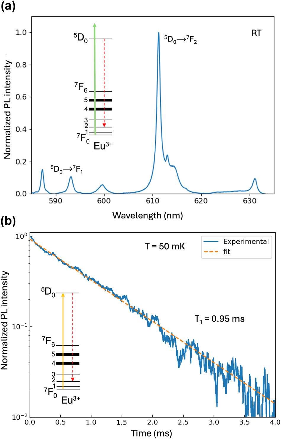
Photoluminescence (PL) spectroscopy of Eu3+ ions in the Y2O3 thin film. (a) Room temperature PL spectrum showing several Eu3+ emission lines including the strong 5D0 →7F2 emission at 611 nm. (b) 5D0 →7F2 PL decay recorded at 50 mK and 611 nm under resonant 7F0 →5D0 excitation at 580.79 nm. The dashed orange line corresponds to a single exponential fit to the data yielding a population lifetime T 1 = 0.95 ms for the 5D0 excited state.
For probing the emission dynamics and optical homogeneous linewidth of Eu3+ ions, the thin film was mounted into a dilution refrigerator equipped with a home-built optical microscopy setup and excited using a tunable dye laser with a 300 kHz linewidth. Full experimental details are given in the Supplementary Materials (SM) document (Section 4). The lifetime (T 1) of the 5D0 excited state was then measured at 50 mK by resonantly exciting the 7F0 →5D0 transition at 580.79 nm (Figure 3(b)). A value of 0.95 ms was obtained by single-exponential adjustment, comparable to bulk Y2O3: Eu3+ radiative lifetime [27]. This result highlights the good crystalline quality and low defect content of the film, and establishes a lower limit to the optical homogeneous linewidth of 170 Hz (1/2πT 1).
The optical inhomogeneous line of the 7F0 ↔5D0 transition is displayed in Figure 4(a). We observe a full width at half maximum (FWHM) of 132 GHz by monitoring the PL emission intensity at 611 nm as a function of the excitation wavelength. The measurement was carried out at three different excitation powers to rule out power broadening effects. The measured inhomogeneous linewidth is significantly broader than that expected for a nominal concentration of 2 %, which would be less than 40 GHz. This expectation is based on previous spectroscopic studies conducted on high-quality bulk Y2O3: Eu3+ samples with varying doping concentrations [28], assuming a linear trend with increasing concentration [29]. The measured linewidth of 132 GHz is comparable to that observed in annealed polycrystalline Y2O3: Eu3+ thin films with the same Eu3+ concentration (2 % at.) deposited via DLI-CVD. This broadening reveals the presence of a substantial number of static defects in the film, likely attributed to strain induce by the annealing treatment [22]. The 2 % Eu3+ concentration spectrally distributed over the 132 GHz lead to an average of ∼60 emitters per excitation bandwidth (300 kHz) in a diffraction-limited excitation volume. The intensity of the detected PL signals indicates however that we are collecting photons from at least 103 ions which we attribute to a larger excitation volume and power broadening effects (see Section 5 discussion in SM).
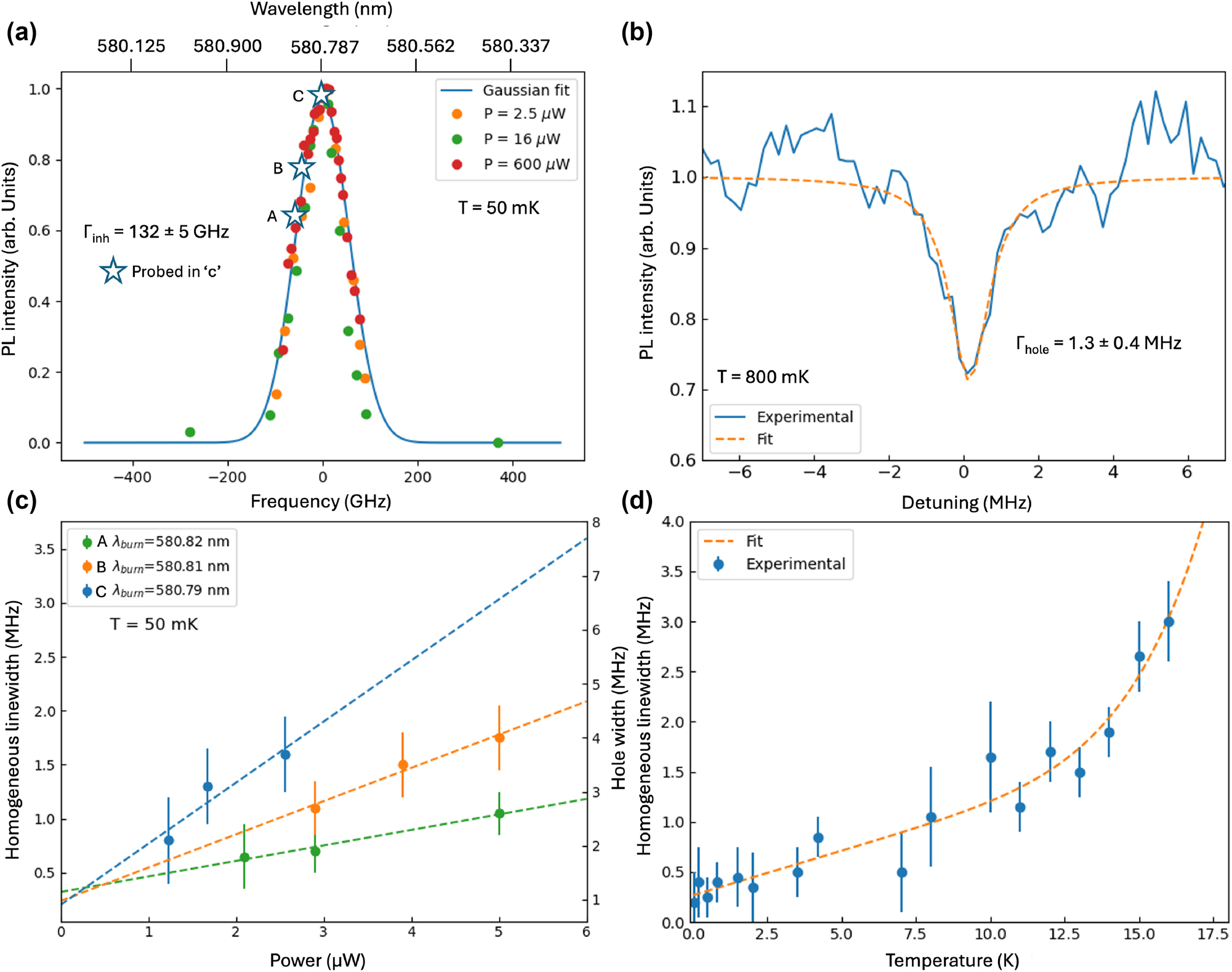
High resolution and coherent optical characterizations at mK temperature. (a) Inhomogeneous linewidth for the 5D0 →7F0 transition measured at three different excitation powers by scanning the excitation wavelength while monitoring the 5D0 →7F2 emission at 611 nm. A Gaussian curve fit to the data yields a full width at half maximum (FWHM) of 132 ± 5 GHz. The stars indicate spectral position within the linewidth of the ions probed in (c). (b) Spectral hole burned at 580.787 nm at a temperature of 800 mK (blue solid line). The dashed orange line correspond to a Lorentzian curve fit to the data yielding a hole width of 1.3 ± 0.4 MHz. (c) Homogeneous linewidth (left axis) and hole width (right axis) as a function of burn power measured at three different frequencies within the inhomogeneous line (see (a)). (d) Homogeneous linewidth as a function temperature (blue points). The dashed orange line corresponds to a fit to these data using eq. (1).
The optical homogeneous linewidth (Γ h ) exhibited by the Eu3+ ions in the film was finally probed by persistent spectral hole burning. Spectral holes presenting a narrow width of the order of 1 MHz were recorded (Figure 4(b)), a value which is one order of magnitude lower than spectral holes measured at 3 K in polycrystalline CVD Y2O3: 2 % Eu3+ thin films [20], [22]. This result suggests that the epitaxial ordering achieved in the present CVD film goes along with a significantly lower decoherence probably due to a lesser amount of defects [30]. To gain a further insight into the dynamical mechanisms limiting Γ h , spectral holes were measured at different spectral positions within the inhomogeneous line (labelled A, B and C and indicated by star symbols in Figure 4(a)) and also using different excitation powers. The obtained hole widths (Γhole) and resulting homogeneous linewidths (Γ h ), estimated as Γhole/2-Γlaser, with Γlaser = 300 kHz, are displayed in Figure 4(c). A linear Γ h broadening is observed when increasing power, but with a slope that decreases when the excitation wavelength is moved away from the center of the inhomogeneous line (C at 580.79 nm) towards the side (A at 580.82 nm). In other words, the observed power broadening effect is stronger when the excited ion ensemble increases, revealing an excitation-induced contribution to Γ h in the Y2O3: Eu3+ film proportional to the number of excited ions [31]. Yet, a power-independent Γ h between 200 and 300 kHz can be extrapolated for all probed excitation wavelengths at the zero power limit, showing no significative differences in the optical coherence properties of different ion ensembles within the inhomogeneous line. The evolution of Γ h with temperature was also measured and is given in Figure 4(d). The obtained Γ h (T) was fitted by
where Γ0 represents the temperature-independent contribution to Γ h , α is the coupling constant to the so-called two-level systems (TLS), or dynamical disorder modes characterized by a linear temperature dependence [32], and β the coupling constant to two-phonon Raman scattering processes [29]. Best-fit parameters to the data yield Γ0 = 270 ± 87 kHz, α = 89 ± 14 kHz/K and β = 5 ± 1 × 10⁶ kHz/K7. The TLS contribution, indicative of the amount of dynamic disorder, is here 5 times lower than in previously reported polycrystalline CVD Y2O3: 2 % Eu3+ thin films [22] while comparable to that observed in optimized Y2O3: Eu3+ (0.3 % at.) nanoparticles of 100 nm size also probed by spectral hole burning (α = 132 kHz/K) [32].
3 Discussion and conclusions
In this manuscript, we report a method to obtain rare-earth doped Y2O3 thin films with enhanced optical properties for quantum technology applications. Due to a low lattice mismatch to Y2O3 (1.9 %), and the possibility to grow it by MBE with high crystalline quality, epitaxial Gd2O3 on Si offers an ideal buffer layer that could be overgrown by our active Y2O3:REI layer using CVD. This hybrid MBE-CVD approach allows preventing unwanted oxidation of the Si substrate while still benefiting from the simplicity and verstatility of CVD to grow complex thin film architectures. This approach could be extended to other epitaxial buffer oxide layers on Si, including Y2O3 itself, which can be also grown by MBE [11], [33], while offering the perfect lattice matching for the DLI-CVD growth [11], [33]. The only strong requirement is a good quality MBE buffer to succeed in the epitaxy. This means that the buffer itself must epitaxial and present a smooth surface. Our approach can also be extended to other REIs. In particular, Er3+ offers an optical transition in the telecom band directly compatible with Si photonic circuits (PCs) [4]. The transition wavelength of Eu3+, on the other hand, can be addressed using other photonic architectures such as Si3N4 resonators on top of the CVD film [34]. Coupling to tunable Fabry–Perot fiber cavities would be also possible [35], [36], by removing all or part of the Si substrate [19].
In conclusion, by the proposed hybrid CVD-MBE thin film fabrication approach, we are indeed combining the best features and advantages of both techniques. This is in particular evidenced by the significant step forward in terms of optical coherence properties achieved in this work for the active Y2O3: Eu3+ thin film, showing an optical homogeneous linewidth as narrow as 270 kHz assessed by persistent spectral hole burning. This accounts for a ten-fold improvement with respect to previous reports on the same material, opening promising perspectives for further developments in the field of quantum-grade REI thin films.
Funding source: QuanTIP
Funding source: FACCTS program
Funding source: European Commission
Award Identifier / Grant number: 820391
Funding source: Agence Nationale de la Recherche
Award Identifier / Grant number: ANR-20-CE09-0022-01
Acknowledgments
We thank Aurélien Debelle (IC2MP – Université de Poitiers) for providing the Gd2O3/Si substrate for this study.
-
Research funding: This project has received funding from the European Union Horizon 2020 research and innovation program under grant agreement no. 820391 (SQUARE), from the French Agence Nationale de la Recherche under grant ANR-20-CE09-0022-01 (UltraNanOSpec), from the CNRS Prime 80 grant (Hyboxi) and, the regional network on quantum technologies of Ile-de-France region (QuanTip) are gratefully acknowledged for funding. This project was also partially funded by the research collaboration program between the University of Chicago and CNRS, and the France and Chicago Collaborating in The Sciences (FACCTS) program.
-
Author contributions: DS: Conceptualization; Data curation; Formal analysis; Investigation; Methodology; Validation; Visualization; Supervision; Writing original draft; Writing review & editing. NH: Conceptualization; Sample fabrication and characterization; Data curation; Writing – review & editing. RB: XRD analysis; Writing – review & editing. AB: Sample characterization; Writing – review & editing. AF: Conceptualization; Investigation; Writing – review & editing. AT: Investigation; Validation; Writing – review & editing. TZ: Conceptualization; Funding acquisition; Methodology; Project administration; Validation; Writing – review & editing. PG: Conceptualization; Funding acquisition; Methodology; Project administration; Resources; Validation; Writing – review & editing. AT: Conceptualization; Funding acquisition; Methodology; Project administration; Resources; Supervision; Validation; Writing – review & editing. All authors have accepted responsibility for the entire content of this manuscript and approved its submission.
-
Conflict of interest: Authors state no conflict of interest.
-
Informed consent: Informed consent was obtained from all individuals included in this study.
-
Data availability: The datasets generated during and/or analyzed during the current study are available from the corresponding author on reasonable request.
References
[1] R. Hull, J. Parisi, R. M. Osgood, H. Warlimont, G. Liu, and B. Jacquier, Eds. Spectroscopic Properties of Rare Earths in Optical Materials, vol. 83 of Springer Series in Materials Science, Berlin, Heidelberg, Springer, 2005.10.1007/3-540-28209-2Search in Google Scholar
[2] P. Goldner, A. Ferrier, and O. Guillot-Noël, “Chapter 267 - rare earth-doped crystals for quantum information processing,” in Handbook on the Physics and Chemistry of Rare Earths, vol. 46, J.-C. G. Bünzli and V. K. Pecharsky, Eds., The Netherlands, Elsevier, 2015, pp. 1–78.10.1016/B978-0-444-63260-9.00267-4Search in Google Scholar
[3] R. M. Macfarlane, A. Arcangeli, A. Ferrier, and P. Goldner, “Optical measurement of the effect of electric fields on the nuclear spin coherence of rare-earth ions in solids,” Phys. Rev. Lett., vol. 113, no. 15, p. 157603, 2014. https://doi.org/10.1103/physrevlett.113.157603.Search in Google Scholar
[4] A. M. Dibos, M. Raha, C. M. Phenicie, and J. D. Thompson, “Atomic source of single photons in the telecom band,” Phys. Rev. Lett., vol. 120, no. 24, p. 243601, 2018. https://doi.org/10.1103/physrevlett.120.243601.Search in Google Scholar PubMed
[5] T. Zhong, et al.., “Nanophotonic rare-earth quantum memory with optically controlled retrieval,” Science, vol. 357, no. 6358, pp. 1392–1395, 2017. https://doi.org/10.1126/science.aan5959.Search in Google Scholar PubMed
[6] J. G. Bartholomew, et al.., “On-chip coherent microwave-to-optical transduction mediated by ytterbium in YVO4,” Nat. Commun., vol. 11, no. 1, p. 3266, 2020. https://doi.org/10.1038/s41467-020-16996-x.Search in Google Scholar PubMed PubMed Central
[7] M. Lei, et al.., “Quantum thermalization and Floquet engineering in a spin ensemble with a clock transition,” 2024, arXiv:2408.00252.Search in Google Scholar
[8] Y. Jia, et al.., “Integrated photonics based on rare-earth ion-doped thin-film lithium niobate,” Laser Photonics Rev., vol. 16, no. 9, p. 2200059, 2022, https://doi.org/10.1002/lpor.202200059.Search in Google Scholar
[9] A. Gritsch, A. Ulanowski, and A. Reiserer, “Purcell enhancement of single-photon emitters in silicon,” Optica, vol. 10, no. 6, pp. 783–789, 2023. https://doi.org/10.1364/optica.486167.Search in Google Scholar
[10] T. Zhong and P. Goldner, “Emerging rare-earth doped material platforms for quantum nanophotonics,” Nanophotonics, vol. 8, no. 11, pp. 2003–2015, 2019. https://doi.org/10.1515/nanoph-2019-0185.Search in Google Scholar
[11] M. K. Singh, et al.., “Epitaxial Er-doped Y2O3 on silicon for quantum coherent devices,” APL Mater., vol. 8, no. 3, p. 031111, 2020. https://doi.org/10.1063/1.5142611.Search in Google Scholar
[12] N. Kunkel, J. Bartholomew, L. Binet, A. Ikesue, and P. Goldner, “High-resolution optical line width measurements as a material characterization tool,” J. Phys. Chem. C, vol. 120, no. 25, pp. 13725–13731, 2016. https://doi.org/10.1021/acs.jpcc.6b03337.Search in Google Scholar
[13] A. Perrot, et al.., “Narrow optical homogeneous linewidths in rare earth doped nanocrystals,” Phys. Rev. Lett., vol. 111, no. 20, p. 203601, 2013. https://doi.org/10.1103/physrevlett.111.203601.Search in Google Scholar PubMed
[14] K. Karlsson, N. Kunkel, A. Ikessue, A. Ferrier, and P. Goldner, “Nuclear spin coherence properties of 151Eu3+ and 153Eu3+ in a Y2O3 transparent ceramic,” J. Phys. Condens. Matter., vol. 29, no. 12, 2017, https://doi.org/10.1088/1361-648x/aa529a.Search in Google Scholar
[15] R. Fukumori, Y. Huang, J. Yang, H. Zhang, and T. Zhong, “Subkilohertz optical homogeneous linewidth and dephasing mechanisms in Er3+:Y2O3 ceramics,” Phys. Rev. B, vol. 101, no. 21, p. 214202, 2020. https://doi.org/10.1103/physrevb.101.214202.Search in Google Scholar
[16] R. M. Macfarlane and R. M. Shelby, “Sub-kilohertz optical linewidths of the 7F0 ↔ 5D0 transition in Y2O3:Eu3+,” Opt. Commun., vol. 39, no. 3, pp. 169–171, 1981. https://doi.org/10.1016/0030-4018(81)90048-1.Search in Google Scholar
[17] M.-H. Cho, et al.., “Structural characteristics of Y2O3 films grown on oxidized Si(111) surface,” J. Appl. Phys., vol. 89, no. 3, pp. 1647–1652, 2001. https://doi.org/10.1063/1.1337920.Search in Google Scholar
[18] S. C. Choi, et al.., “Epitaxial growth of Y2O3 films on Si(100) without an interfacial oxide layer,” Appl. Phys. Lett., vol. 71, no. 7, pp. 903–905, 1997. https://doi.org/10.1063/1.119683.Search in Google Scholar
[19] S. Gupta, et al.., “Dual epitaxial telecom spin-photon interfaces with correlated long-lived coherence,” 2023, arXiv:2310.07120 [quant-ph].Search in Google Scholar
[20] N. Harada, et al.., “Chemically vapor deposited Eu3+:Y2O3 thin films as a material platform for quantum technologies,” J. Appl. Phys., vol. 128, no. 5, p. 055304, 2020. https://doi.org/10.1063/5.0010833.Search in Google Scholar
[21] I. G. BalaŞa, et al.., “Rare earth-diamond hybrid structures for optical quantum technologies,” Adv. Opt. Mater., vol. 12, no. 31, p. 2401487, 2024. https://doi.org/10.1002/adom.202401487.Search in Google Scholar
[22] N. Harada, et al.., “Controlling the interfacial reactions and environment of rare-earth ions in thin oxide films towards wafer-scalable quantum technologies,” Mater. Adv., vol. 3, no. 1, 2022, https://doi.org/10.1039/d1ma00753j.Search in Google Scholar
[23] G. Niu, G. Saint-Girons, and B. Vilquin, “Chapter 17 – epitaxial systems combining oxides and semiconductors,” in Molecular Beam Epitaxy, M. Henini, Ed., 2nd ed. The Netherlands, Elsevier, 2018, pp. 377–402.10.1016/B978-0-12-812136-8.00018-9Search in Google Scholar
[24] J. Zhang, et al.., “Optical and spin coherence of Er spin qubits in epitaxial cerium dioxide on silicon,” npj Quantum Inf., vol. 10, no. 1, pp. 1–9, 2024. https://doi.org/10.1038/s41534-024-00903-z.Search in Google Scholar
[25] G. Niu, et al.., “Growth temperature dependence of epitaxial Gd2O3 films on Si(111),” Microelectron. Eng., vol. 86, no. 7, pp. 1700–1702, 2009. https://doi.org/10.1016/j.mee.2009.03.107.Search in Google Scholar
[26] M. H. Cho, D. H. Ko, Y. G. Choi, I. W. Lyo, K. Jeong, and C. N. Whang, “Effects of SiO2 overlayer at initial growth stage of epitaxial Y2O3 film growth,” J. Cryst. Growth, vol. 220, no. 4, pp. 501–509, 2000. https://doi.org/10.1016/s0022-0248(00)00835-6.Search in Google Scholar
[27] S. P. Feofilov, et al.., “Modified radiative lifetime of Eu3+ ions in Y2O3 thin films on Al2O3 substrates,” J. Lumin., vol. 230, p. 117754, 2021. https://doi.org/10.1016/j.jlumin.2020.117754.Search in Google Scholar
[28] N. Kunkel, et al.., “Rare-earth doped transparent ceramics for spectral filtering and quantum information processing,” APL Mater., vol. 3, no. 9, p. 096103, 2015. https://doi.org/10.1063/1.4930221.Search in Google Scholar
[29] F. Konz, et al.., “Temperature and concentration dependence of optical dephasing, spectral-hole lifetime, and anisotropic absorption in Eu:Y2SiO5,” Phys. Rev. B, vol. 68, no. 8, p. 085109, 2003. https://doi.org/10.1103/physrevb.68.085109.Search in Google Scholar
[30] S. Liu, D. Serrano, A. Fossati, A. Tallaire, A. Ferrier, and P. Goldner, “Controlled size reduction of rare earth doped nanoparticles for optical quantum technologies,” RSC Adv., vol. 8, no. 65, pp. 37098–37104, 2018. https://doi.org/10.1039/c8ra07246a.Search in Google Scholar PubMed PubMed Central
[31] C. W. Thiel, et al.., “Measuring and analyzing excitation-induced decoherence in rare-earth-doped optical materials,” Laser Phys., vol. 24, no. 10, p. 106002, 2014. https://doi.org/10.1088/1054-660x/24/10/106002.Search in Google Scholar
[32] A. Fossati, D. Serrano, S. Liu, A. Tallaire, A. Ferrier, and P. Goldner, “Optical line broadening mechanisms in rare-earth doped oxide nanocrystals,” J. Lumin., vol. 263, p. 120050, 2023, https://doi.org/10.1016/j.jlumin.2023.120050.Search in Google Scholar
[33] A. Blin, et al.., “Erbium doped yttrium oxide thin films grown by chemical vapour deposition for quantum technologies,” arXiv.2411.10196, 2024.Search in Google Scholar
[34] J. Wang, F. Sciarrino, A. Laing, and M. G. Thompson, “Integrated photonic quantum technologies,” Nat. Photonics, vol. 14, no. 5, pp. 273–284, 2020. https://doi.org/10.1038/s41566-019-0532-1.Search in Google Scholar
[35] B. Casabone, et al.., “Cavity-enhanced spectroscopy of a few-ion ensemble in Eu3+:Y2O3,” New J. Phys., vol. 20, no. 9, p. 095006, 2018. https://doi.org/10.1088/1367-2630/aadf68.Search in Google Scholar
[36] B. Casabone, et al.., “Dynamic control of Purcell enhanced emission of erbium ions in nanoparticles,” Nat. Commun., vol. 12, no. 1, 2021, https://doi.org/10.1038/s41467-021-23632-9.Search in Google Scholar PubMed PubMed Central
Supplementary Material
This article contains supplementary material (https://doi.org/10.1515/nanoph-2024-0682).
© 2025 the author(s), published by De Gruyter, Berlin/Boston
This work is licensed under the Creative Commons Attribution 4.0 International License.
Articles in the same Issue
- Frontmatter
- Editorial
- Quantum light: creation, integration, and applications
- Reviews
- Low-dimensional solid-state single-photon emitters
- Solid-state single-photon sources operating in the telecom wavelength range
- Quantum super-resolution imaging: a review and perspective
- Perspectives
- New opportunities for creating quantum states of light and matter with intense laser fields
- On-chip frequency-bin quantum photonics
- Building photonic links for microwave quantum processors
- Remote quantum networks based on quantum memories
- Sensing with quantum light: a perspective
- Letter
- Electro-optic frequency shift of single photons from a quantum dot
- Research Articles
- Quantum efficiency of the B-center in hexagonal boron nitride
- Localized exciton emission from monolayer WS2 nanoribbon at cryogenic temperature
- Single-photon emitters in PECVD-grown silicon nitride films: from material growth to photophysical properties
- A fiber-pigtailed quantum dot device generating indistinguishable photons at GHz clock-rates
- Sub-MHz homogeneous linewidth in epitaxial Y2O3: Eu3+ thin film on silicon
- Multimodal Purcell enhancement and optical coherence of Eu3+ ions in a single nanoparticle coupled to a microcavity
- All-optical control of charge-trapping defects in rare-earth doped oxides
- Ultra-broadband and passive stabilization of ultrafast light sources by quantum light injection
- Tunable quantum light by modulated free electrons
- Second-harmonic radiation by on-chip integrable mirror-symmetric nanodimers with sub-nanometric plasmonic gap
- Mie metasurfaces for enhancing photon outcoupling from single embedded quantum emitters
- Design and fabrication of robust hybrid photonic crystal cavities
- Enhanced zero-phonon line emission from an ensemble of W centers in circular and bowtie Bragg grating cavities
- Freeform thin-film lithium niobate mode converter for photon-pair generation
- Luminescence thermometry based on photon emitters in nanophotonic silicon waveguides
- Collective single-photon emission and energy transfer in thin-layer dielectric and plasmonic systems
- Description of ultrastrong light–matter interaction through coupled harmonic oscillator models and their connection with cavity-QED Hamiltonians
- Bound polariton states in the Dicke–Ising model
- Collective multimode strong coupling in plasmonic nanocavities
- Improving quantum metrology protocols with programmable photonic circuits
- Fluorescence enabled phonon counting in an erbium-doped piezo-optomechanical microcavity
- Non-perturbative cathodoluminescence microscopy of beam-sensitive materials