Semimetal–dielectric–metal metasurface for infrared camouflage with high-performance energy dissipation in non-atmospheric transparency window
-
Dongjie Zhou


Abstract
The development of novel camouflage technologies is of great significance, exerting an impact on both fundamental science and diverse military and civilian applications. Effective camouflage aims to reduce the recognizability of an object, making it to effortlessly blend with the environment. For infrared camouflage, it necessitates precise control over surface emissivity and temperature to ensure that the target blends effectively with the surrounding infrared background. This study presents a semimetal–dielectric–metal metasurface emitter engineered for the application of infrared camouflage. The metasurface, with a total thickness of only 545 nm, consists of a Bi micro-disk array and a continuous ZnS and Ti film beneath it. Unlike conventional metal-based metasurface design, our approach leverages the unique optical properties of Bi, achieving an average emissivity of 0.91 in the 5–8 μm non-atmospheric transparency window. Experimental results indicate that the metasurface emitter achieves lower radiation and actual temperatures compared to those observed in comparative experiments, highlighting its superior energy dissipation and thermal stability. The metasurface offers advantages such as structural simplicity, cost-effectiveness, angular insensitivity, and deep-subwavelength features, rendering it suitable for a range of applications including military camouflage and anti-counterfeiting, with potential for broad deployment in infrared technologies.
1 Introduction
The basic idea of camouflage is to minimize the detectable signature of an object and enable it to seamlessly blend with its surrounding background [1]. This approach is applicable to various electromagnetic wave bands [2], including the visible [3], [4], infrared [5], [6], and microwave regions [7], [8]. In contrast to visible and microwave bands, infrared surveillance systems typically work in a passive manner by detecting the infrared radiation emitted by objects [9]. Therefore, controlling of thermal radiation of targets plays a crucial role in infrared camouflage against infrared detection. Specifically, in order to achieve effective infrared camouflage for high temperature target, it is necessary for the device to exhibit low emission in specific atmospheric transparency windows (ATWs) [10], such as, 3–5 μm mid-wavelength infrared (MWIR) and 8–14 μm long-wavelength infrared (LWIR) ATW regions. At the meantime, it is normally required that the device should have high emission in non-atmospheric transparency window (non-ATW), such as 5–8 μm region, this would allow the device to reduce its temperature and further decrease the infrared radiation signal [11], [12], [13], [14], [15], [16], [17], [18], [19], [20].
So far, many types of artificially engineered materials have been investigated to developing wavelength-selective emitters for the applications of infrared camouflage based on the above strategy [21], [22], [23], [24], [25], [26], [27], [28], [29], [30], [31]. For example, photonic crystals based on dielectric–metal–dielectric (DMD) film perforated with a two-dimensional periodic aperture array have been exploited for high temperature infrared camouflage [32]. Metal–dielectric–metal (MDM) configuration metasurfaces made of metals such as gold (Au), silver (Ag), or aluminum (Al) have been proposed and demonstrated for infrared camouflage with thermal management [17], [18], [19]. Although these approaches have been successfully demonstrated to control the thermal emission of objects and realize impressive infrared camouflage effect, the performance, particularly in terms of energy dissipation efficiency in the non-ATW still could be improved.
In this study, we introduce a novel paradigm of semimetal–dielectric–metal (SMDM) metasurface emitter with high energy dissipation efficiency in the non-ATW for infrared camouflage. The SMDM metasurface consists of a layer of semimetal bismuth (Bi) micro-disk array, and a continuous titanium (Ti) film, separated by a zinc sulfide (ZnS) dielectric spacer. In contrast to previous works [33], [34], [35], [36], [37], [38], [39], semimetal Bi incorporated with Ti is employed instead of metals, such as, Au, Ag, and Al in our design. Semimetal Bi exhibits a unique optical response, which has negative values of the real part (ε real ) of permittivity in the visible range [40], [41], similar to that of noble metals, while in the infrared region (see Section S1 in Supplementary Material for more detail), it possesses high positive ε real values behavior as a lossy dielectric medium [42], [43]. By exploiting the overlapping of hybrid plasmonic resonances from the patterned Bi-based metasurface, the proposed metasurface emitter achieves an average emissivity of 0.91 in the 5–8 μm non-ATW, and exhibits a reduced emissivity of 0.72 in the MWIR ATW and 0.34 in the LWIR ATW, respectively. Experimental verification of the energy dissipation capability of the SMDM metasurface emitter revealed lower radiation and actual temperatures compared to samples lacking efficient emission capabilities at non-ATWs. Compared to a low emissivity metal film, the radiation temperature of the metasurface emitter is not much different from that the metal film, but the actual temperature is significantly lower, demonstrating its efficient energy dissipation capability and thermal stability. The proposed SMDM metasurface offers several advantages over previous designs, including a simpler structure, cost-efficiency, large-area fabrication, deep-subwavelength features, and angular insensitivity. These findings suggest promising applications that extend beyond infrared camouflage, including enhancements in thermal imaging [44], infrared anti-counterfeiting [45], and mid-infrared biological sensing [46].
2 Results and discussion
Figure 1(a) illustrates schematic diagrams of the proposed SMDM metasurface selective emitter, which is basically comprised of three layers. The first layer is made of a periodic array of Bi micro-disks. D and t Bi represent the diameter and the thickness of the Bi micro-disk, respectively, and P signifies the periodicity of the micro-disk array. The second and third layers are composed of ZnS and Ti films. Their thicknesses are denoted by t ZnS and t Ti , respectively.

SMDM metasurface emitter for infrared camouflage concept and fabrication. (a) Illustration schematically depicting the proposed SMDM metasurface emitter. (b) Emissivity spectra for the metasurface emitter, where the simulation results (blue line) and experimental measurements (red dot line) are presented. These spectra were obtained with fixed parameters: t Bi = 25 nm, D = 2.4 μm, P = 3.3 μm, t ZnS = 400 nm and t Ti = 120 nm. The comparison includes the ideal low emissivity infrared stealth spectra (black dash line) and the atmospheric transmission spectra (blue-shaded area). (c) Top-view and tilt-view SEM images of the experimental sample. (d) Optical images of the experimental sample.
To determine the emission performance of the proposed emitter in the non-ATW, full-wave numerical simulations were conducted to investigate the dependence of emissivity on various geometrical factors. According to Kirchhoff’s law of thermal radiation, the emissive and absorptive properties of the structures are equal under thermal equilibrium. The emissivity (E) can be calculated as E = A = 1 − R − T, where A, R, and T represent the absorptance, reflectance, and transmittance of the proposed SMDM metasurface, respectively. The solid lines of Figure 2(a)–(d) show the simulated emissivity spectra for a series of Bi micro-disk thicknesses (t Bi = 0, 15, 25, and 35 nm) at normal emission direction, with fixed other parameters as D = 2.4 μm, P = 3.3 μm, t ZnS = 400 nm, and t Ti = 120 nm. When the Bi micro-disk array is absent (t Bi = 0 nm), the structure exhibits only one narrow resonant mode with the center wavelength of 3.9 μm located at MWIR ATW region. As the thickness of the Bi micro-disk (t Bi ) increases, the center wavelength of resonant mode is redshifted to the non-ATW region, accompanied by the emergence of another emission resonance in the longer wavelength of this region. The solid lines of Figure 2(e) and (f) showcase the simulated emissivity spectra for four different diameters of the Bi micro-disk (D = 3.3, 2.85, 2.4, and 1.95 μm) at normal emission direction, with other parameters taken as t Bi = 25 nm, P = 3.3 μm, t ZnS = 400 nm, and t Ti = 120 nm. When the top Bi micro-disk array becomes a continuous Bi thin film, namely, D = 3.3 μm, only one resonance emission peak located at the boundary between the LWIR ATW and non-ATW regions is observed as well. As the diameter D decreases, the longer wavelength emission peak gradually blueshifts and overlaps with that of the shorter wavelength, thus forming a wide emission band covering the range of the non-ATW. The relationships between the emission properties and other geometrical parameters are also investigated and presented in Figure S2 in Supplementary Material.
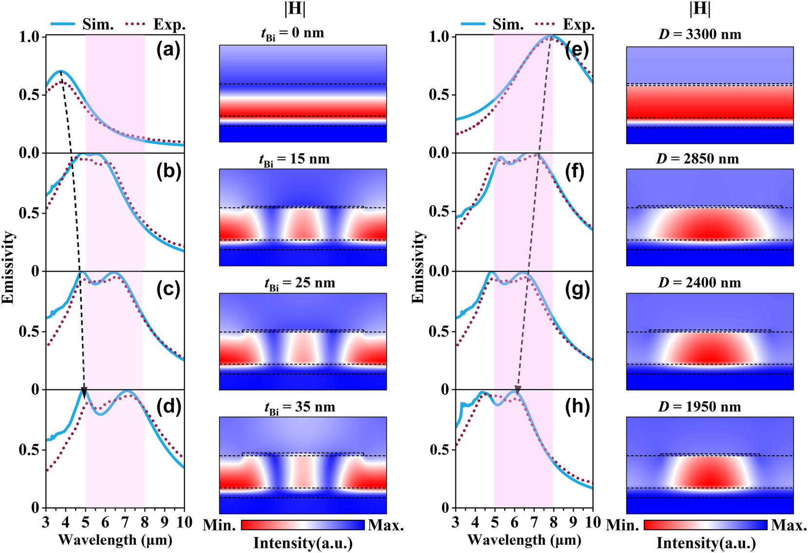
The relationship between the geometrical parameters of the Bi micro-disk with the optical response and resonance of SMDM emitter. (a–d) Comparison of simulated and experimental emissivity spectra for a series of SMDM metasurfaces with varying thicknesses of the Bi micro-disk (t Bi = 0, 15, 25, and 35 nm), fixed D = 2.4 μm and accompanied by the magnetic field distribution of the resonant mode at shorter wavelengths. (e–h) Comparison of simulated and experimental emissivity spectra for a series of SMDM metasurfaces with varying diameters of the Bi micro-disk (D = 3,300, 2,850, 2,400, and 1,950 nm), fixed t Bi = 25 nm and accompanied by the magnetic field distribution of the resonant mode at longer wavelengths. All results fixed the parameters as t ZnS = 400 nm and P = 3.3 μm.
To understand the nature of the proposed SMDM structure, we simulated the electromagnetic field distributions for each emission peak wavelength and plotted the corresponding magnetic field distribution in the right column of each emission spectrum in Figure 2 (more details of field distributions are presented in Figure S3 of Supplementary Material). For the cases of t Bi = 0 nm (see Figure 2(a)) and D = 3.3 μm (see Figure 2(e)), the structures composed of dielectric thin film(s) on top of a metallic reflector belong to typical Gires–Tournois resonator configuration [47], [48], [49], and the high emission/absorption peaks are attributed to the excitation of optical asymmetric Fabry–Perot–type interference resonance modes [50], [51], [52]. For the longer wavelength resonances, as shown in Figure 2(f)–(h), the magnetic field is strongly localized beneath the Bi micro-disk, it looks similar to the fundamental localized magnetic resonance supported by conventional MDM structure. For the shorter wavelength resonances (see Figure 2(b)–(d)), the magnetic field is concentrated not only under the Bi micro-disk but also in the area between two adjacent Bi micro-disks, the field profile exhibits the characterization of both fundamental and high-order plasmonic modes (more details of coupling of the cavity and micro-disk are presented in Section S4 of Supplementary Material). These results mean that such broadband emission/absorption originates from the contribution of hybrid multiplex plasmonic resonances.
To experimentally validate our idea, the proposed structures were fabricated using a combination of electron beam evaporation and laser lithography techniques (see Material and methods for more details of sample fabrication). The measured emissivity spectra of the fabricated emitters are correspondingly shown in Figure 2 as short-dotted lines. Good agreements are found by comparing the experimental spectra with the theoretical simulations. Figure 1(b) highlights the simulated and measured emission spectra of an SMDM metasurface emitter (denoted by “SMDM-S1”) with the optimal geometrical parameters of t Bi = 25 nm, D = 2.4 μm, P = 3.3 μm, t ZnS = 400 nm and t Ti = 120 nm. The theoretical and experimental results show that the SMDM-S1 device exhibits an average emissivity of 0.91 within the non-ATW, 0.72 in the MWIR ATW and 0.34 in the LWIR ATW region. The morphology of the metasurface was characterized by a scanning electron microscope (SEM). As shown in Figure 1(c), the images show a uniformly periodic distribution of the Bi-based metasurface. Notably, there is some undulating surface topography on the Bi micro-disks, characterized by nanometer-level roughness introduced during the growth process. Figure 1(d) shows a photograph of the wafer-scale sample with micro-disk arrays, where the colored portion of the sample represents the structural region.
Table 1 describes the comparison of some recent research works in the field of infrared camouflage with thermal management. It notes that the proposed metasurface exhibits outstanding energy dissipation capability in the non-ATW region while maintaining excellent subwavelength thickness characteristics. This achievement is strongly related to the unique optical properties of Bi (with high refractive index and large absorption coefficient, more details are presented in Section S1 of Supplementary Material) and Ti (possessing strong optical absorption at the shorter wavelengths) materials [53] within the wavelength range of interest, which is challenging to achieve by using conventional metamaterials [14], [15], MDM metasurfaces [17], [18], [19], [20], [21], and promising that our device has great application potential in infrared camouflage. Furthermore, it’s important to note that while our proposed metasurface exhibits exceptionally high emissivity in the non-ATW region, its performance in the MWIR ATW region does not fully exceed that of previous studies. This limitation can be addressed by fine-tuning the structural parameters, as detailed in Figures S2 and S5 of the Supplementary Material. Moreover, since the proportion of mid-wave infrared radiation is relatively small at lower operating temperatures, our proposed SMDM device is suitable for LWIR camouflage applications at temperatures between 300 and 500 K. (see Section S5 in Supplementary Material for more details).
Comparison of the performance of infrared camouflage with thermal management.
| Ref. | Materials | Structure | Thickness | Thermal camouflage | Thermal Management | |
|---|---|---|---|---|---|---|
| ɛ 3–5 μm | ɛ 8–14 μm | ɛ 5–8 μm | ||||
| SMDM | Ti/ZnS/Bi | Metasurface | 0.545 μm | 0.72 | 0.34 | 0.91 |
| [15] | Al2O3/AZO NPs | Metamaterials | 1.2 μm | 0.11 | 0.2 | 0.81 |
| [17] | OPA/Cu | Metamaterials | 1 μm | 0.1 | 0.21 | ∼0.3 |
| [18] | Au/GST/Si | Metasurface | 1.25 μm | 0.69 | 0.27 | 0.72 |
| [19] | Au/ZnS/Au | Metasurface | 0.6 μm | 0.08 | 0.07 | 0.18 |
| [20] | Al/SiO2/Al | Metasurface | 0.62 μm | 0.21 | 0.19 | 0.43 |
| [21] | Au/SiO2/Au/PI | Metasurface | 0.545 μm | 0.14 | 0.08 | 0.31 |
| [22] | Au/Polymide/Au | Metasurface | 0.43 μm | 0.19 | 0.07 | 0.42 |
| [23] | Ag/Ge | 4-layers MFS | 1 μm | 0.17 | 0.31 | 0.82 |
| [24] | SiO2/Ge/ZnS/Pt/Au | 8-layers MFS | 4.4 μm | 0.21 | 0.16 | 0.54 |
| [25] | SiO2/TiO2/Ge | 12-layers MFS | 4.37 μm | 0.14 | 0.21 | 0.86 |
| [26] | Ge/ZnS | 11-layers MFS | 6.73 μm | 0.11 | 0.12 | 0.61 |
| [27] | Ge/YbF3 | 14-layers MFS | 8.49 μm | 0.06 | 0.01 | 0.68 |
To provide further theoretical insights, additional numerical simulations and calculations were performed. Figure 3(a) shows the normalized power loss spectra for the total and each component of the SMDM-S1. In our structure, the energy dissipation contributions from the Ti layer and the Bi micro-disk vary across different wavelength ranges. Specifically, for shorter wavelengths of 5–5.4 μm, the Ti layer accounts for a larger portion of the energy dissipation, contributing 44 % of the total, while the Bi micro-disk contributes 37 %. In contrast, for the longer wavelength range of 5.4–8 μm, this trend reverses, with the Bi micro-disk dominating dissipation at 66 %, while the Ti layer contributes only 27 %. Overall, in the 5–8 μm range, the Bi micro-disk represents the largest share of energy dissipation at 62 %, compared to 30 % from the Ti layer. Figure 3(b) depicts the distributions of power loss density (W/m2) at the two emission peak wavelengths of 5.02 μm and 6.76 μm. As expected, the absorption at the longer wavelength is mostly due to the Bi micro-disk, while, at the shorter wavelength which is determined by both the Bi micro-disk and the Ti thin film. Moreover, we examined why the SMDM-S1 metasurface exhibits highly efficient absorption over the range of non-ATW. Given that the thickness of the 120 nm titanium (Ti) film in the bottom layer is sufficient to prevent light transmission and ensure that all energy dissipation occurs within the structure, the objective of maximizing absorption and emission translates into minimizing reflection. This relationship can be effectively analyzed through the optical impedance (Z). Figure 3(c) shows the optical impedance of the SMDM-S1 metasurface on a Smith impedance chart (see Section S6 in Supplementary Material for the details of the numerical computations). The center point of the chart corresponds to a device with Z = 1, indicating that the impedance of the device is ideally matched to the free space impedance, no incident light energy will be reflected R = 0 and A = 1. The magenta, brown, and celeste short-dotted circles represent the impedances as A = 0.95, 0.9, and 0.85, respectively. It is observed that the optical impedance of the SMDM-S1 metasurface falls within the circle of A = 0.9 over the wavelengths from 5 μm to 7.6 μm, the condition of impedance matching is reasonably well satisfied.
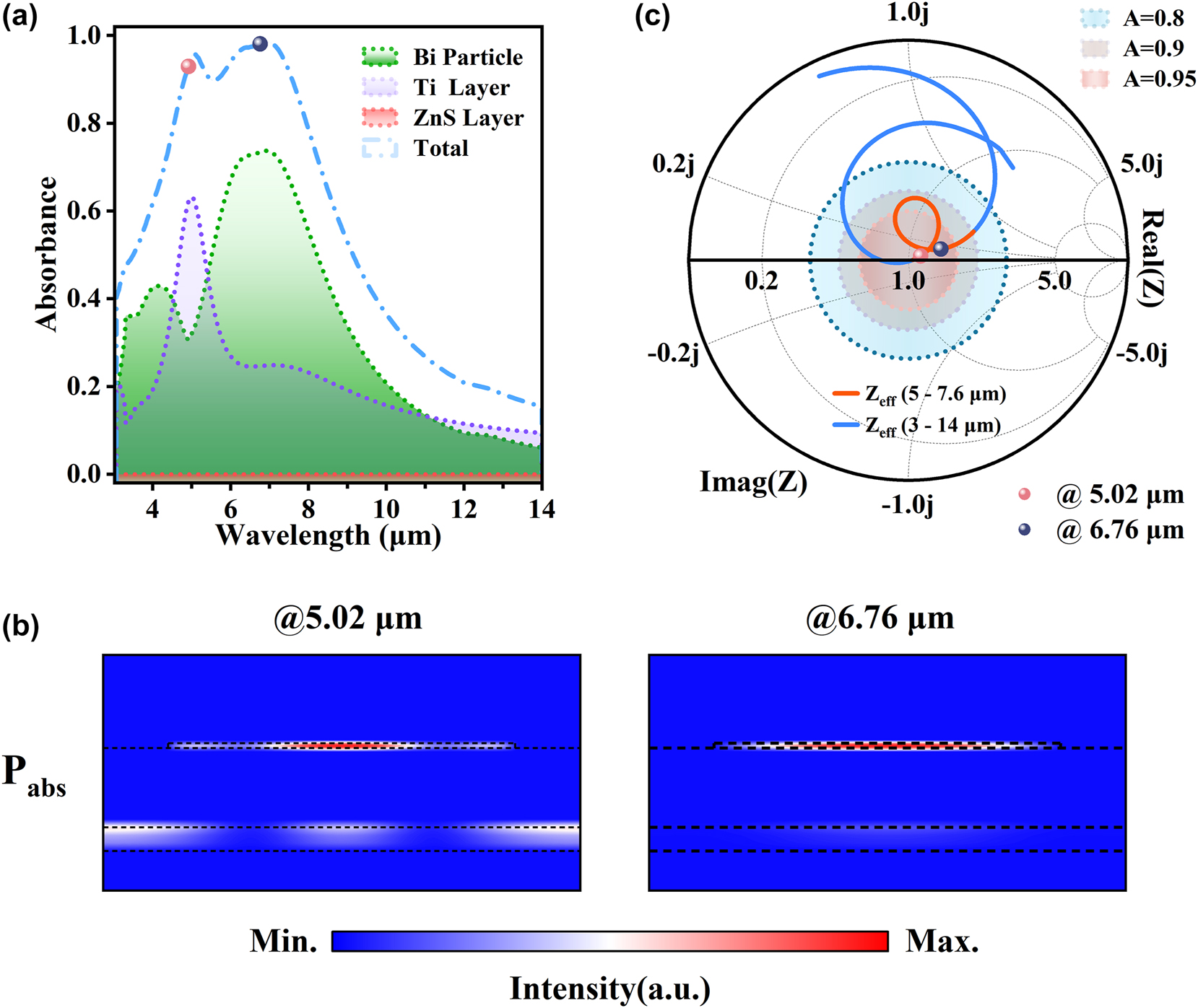
Power dissipation mechanism and optical impedance of the ‘SMDM-S1’ metasurface. (a) The normalized power loss spectra for the total and individual components of the SMDM-S1, with fixed thicknesses of Ti, ZnS, and Bi at 120 nm, 400 nm, and 25 nm, respectively, alongside a fixed period and diameter of the Bi micro-disk at 3.3 μm and 2.4 μm. (b) The normalized power loss density at the two resonant wavelengths of 5.02 μm and 6.76 μm. (c) The optical impedance (Z) of the SMDM-S1 metasurface across the wavelength range of 3–14 μm (blue line), with emphasis on the impedance where A > 0.9 (red line). The magenta, brown, and celeste short-dotted circles represent the impedances as A = 0.95, 0.9, and 0.85, respectively.
The angular dependence of infrared emission properties of the proposed metasurface was also investigated. Figure 4(a)–(c) displays the calculated emissivity (unpolarized, s-polarized, p-polarized) as a function of wavelength and emissive angle for the SMDM-S1 metasurface. The corresponding experimental results are shown in Figure 4(d)–(f). Both theoretical and experimental results show that the broadband selective emission is nearly independent of the emissive angle. The average emissivity in non-ATW remains 0.8 even at the emissive angle up to ∼60° (see Figure S7 in Supplementary Material). The feature endows the metasurface with omnidirectional energy dissipation ability in the non-ATW.
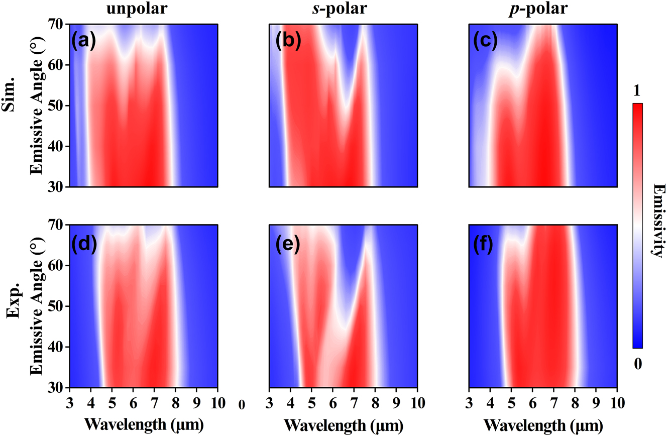
Angular dependences of optical properties of the proposed emitter. (a–c) Simulated and (e–f) experimentally measured emissivity spectra of the SMDM-S1 metasurface as functions of wavelength and emissive angle for unpolarized, s-polarized, and p-polarized light, respectively.
To verify the advantages brought by the selective emission in non-ATW, thermal management performances of the proposed metasurface were evaluated under different situations. The bottom panel of Figure 5(a) illustrates a schematic of the SMDM-S1 metasurface selective emitter used for the thermal management evaluation, which is surrounded by two areas. The inner area (denoted by Ref. 1) consists of three layers of Bi, ZnS, and Ti films that has the same average emissivity in LWIR ATW (E Ref. 1: 8–14 μm = 0.34) as the SMDM-S1 but much lower emissivity in non-ATW (E Ref. 1: 5–8 μm = 0.14). The outer area (denoted by Ref. 2) is composed of only one layer of Ti film, and the emissivity of both LWIR ATW (E Ref. 2: 8–14 μm = 0.09) and non-ATW (E Ref. 2: 5–8 μm = 0.11) is much lower than the SMDM-S1 metasurface (details of the reference samples are presented in Figure S8 in the Supplementary Material). The metasurface device was mounted on a hot plate which is electrically heated by a DC power supply system, as schematically shown in the top panel of Figure 5(a). Thermal infrared images were taken during the thermal measurement by an infrared camera with operating wavelength ranging from 8 μm to 14 μm. The emissivity of the camera was initially set to 0.95 (see Section S9 in the Supplementary Material for more information).
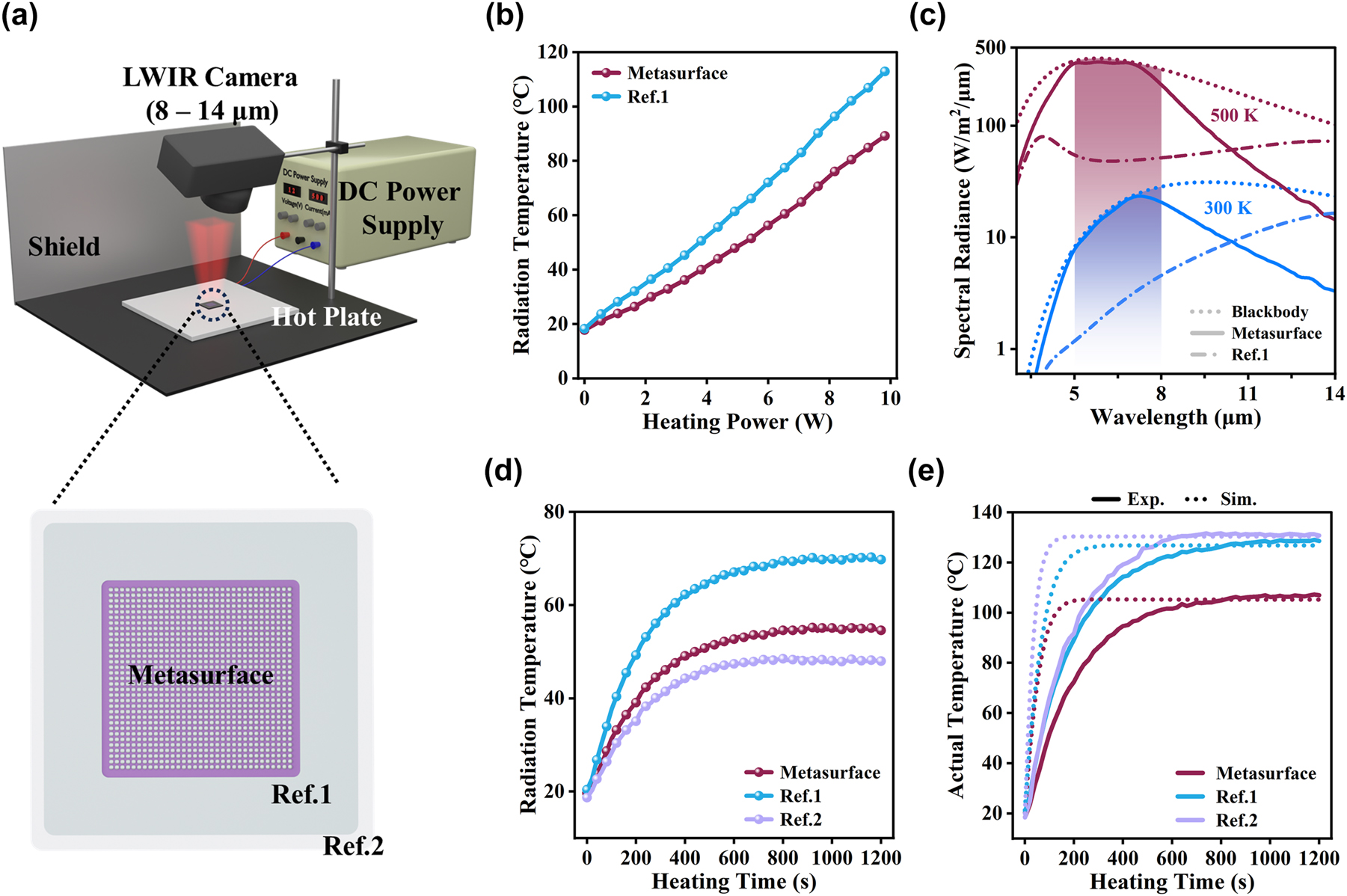
Experimental and simulation validation of the SMDM metasurface emitter thermal management performance. (a) Schematic illustration comparing the experimental setup and fabricated sample of the metasurface, Ref. 1, and Ref. 2. (b) Radiation temperature variation with heating power for the metasurface (reddish brown) and Ref. 1 (sky blue). (c) Spectral radiation of the metasurface (solid line), Ref. 1 (dash-dotted line), blackbody (dotted line), and ideal surface (shaded area) at 300 K (sky blue) and 500 K (reddish brown). (d) Average radiation temperatures of the metasurface, Ref. 1, and Ref. 2 (purplish grey) variation with heating time. (e) Average actual temperatures of the metasurface, Ref. 1, and Ref. 2 (purplish grey) variation with heating time both simulation (dotted line) and experiment (solid line).
Figure 5(b) shows the radiation temperature results for the SMDM-S1 metasurface emitter and the control sample Ref. 1 under different heating powers. As can be observed, the radiation temperature of the metasurface emitter is always lower than that of the Ref. 1 control sample, and the temperature difference increases with the increase of heating power. At a heating power of 9.8 W, the temperature difference can be as high as ∼25 °C. This phenomenon is mainly attributed to the difference in energy dissipation capacity between the SMDM-S1 metasurface and Ref. 1 in the non-ATW region. Figure 5(c) shows the spectral radiance of the SMDM-S1 metasurface and Ref. 1 at temperatures of 300 K and 500 K. For comparison, the spectral radiance of the blackbody is also plotted in Figure 5(c). At 300 K, the radiation power densities of the metasurface and the reference sample Ref. 1 within the 8–14 μm LWIR ATW region are 57.61 W/m2 and 60.1 W/m2; for the 5–8 μm non-ATW, the radiation power densities of the metasurface and Ref. 1 are 52.97 W/m2 and 7.91 W/m2, respectively. At 500 K, the metasurface and the reference sample Ref. 1 have radiation power densities of 400.08 W/m2 and 383.69 W/m2 respectively in the LWIR ATW, and 1,038.03 W/m2 and 149.82 W/m2 respectively in the non-ATW. It notes that the radiative capacity of the metasurface is very close to that of Ref. 1 in the LWIR ATW, however, in the non-ATW, the radiation capacity of the metasurface is much stronger than that of the reference sample. Radiative cooling induced by such strong energy dissipation leads to a lower temperature of the metasurface than the reference sample. Moreover, with the increase of temperature, the greater the difference in radiation power between the metasurface and Ref. 1, this is why the radiation temperature difference between the two becomes larger as the heating power increases.
Figure 5(d) shows the radiation temperature results of the SMDM-S1 metasurface emitter and the control samples Ref. 1 and Ref. 2 according to heating time for a fixed heating power of 6 W. Figure 6(a)–(e) display the infrared images (captured by the infrared camera with the emissivity of 0.95) and the corresponding photographs of this measurement at different temperature stages (6(a, b): initial state (room temperature); 6(c, d): intermediate state temperature; 6(e): steady state temperature). The radiation temperature values are retrieved at the positions labeled by the stars in Figure 6(b), (d), (e). The solid lines of Figure 5(e) show the actual temperature results of the SMDM-S1 metasurface emitter and the reference samples Ref. 1 and Ref. 2 according to heating time for a fixed heating power of 6 W, which are obtained by changing the infrared camera emissivity to 0.34 for the metasurface emitter and Ref. 1 (see Figure 6(f)), and 0.09 for the sample Ref. 2 (see Figure S10 in Supplementary Material). To confirm these results, heat transfer numerical simulations were performed, and the corresponding results are presented in Figure 5(e) as short-dotted lines (see Section S11 in Supplementary Material for more details). The theoretical results for the steady state temperature of the three cases are in good agreement with the experimental values. As shown in Figure 5(d) and (e), both the radiation temperature and actual temperature of Ref. 1, as expected, are higher than the metasurface emitter. Although Ref. 2 exhibits a lower radiation temperature than the metasurface emitter, its actual temperature (130.7 °C) is much higher than of the metasurface emitter (106.0 °C) at the steady state, this can yield thermal instability of the system. In other words, the proposed metasurface emitter can not only be utilized for camouflage by reducing the infrared signature in the ATW but also offers better thermal stability to the target due to its superior radiative cooling capacity through energy dissipation in the non-ATW.
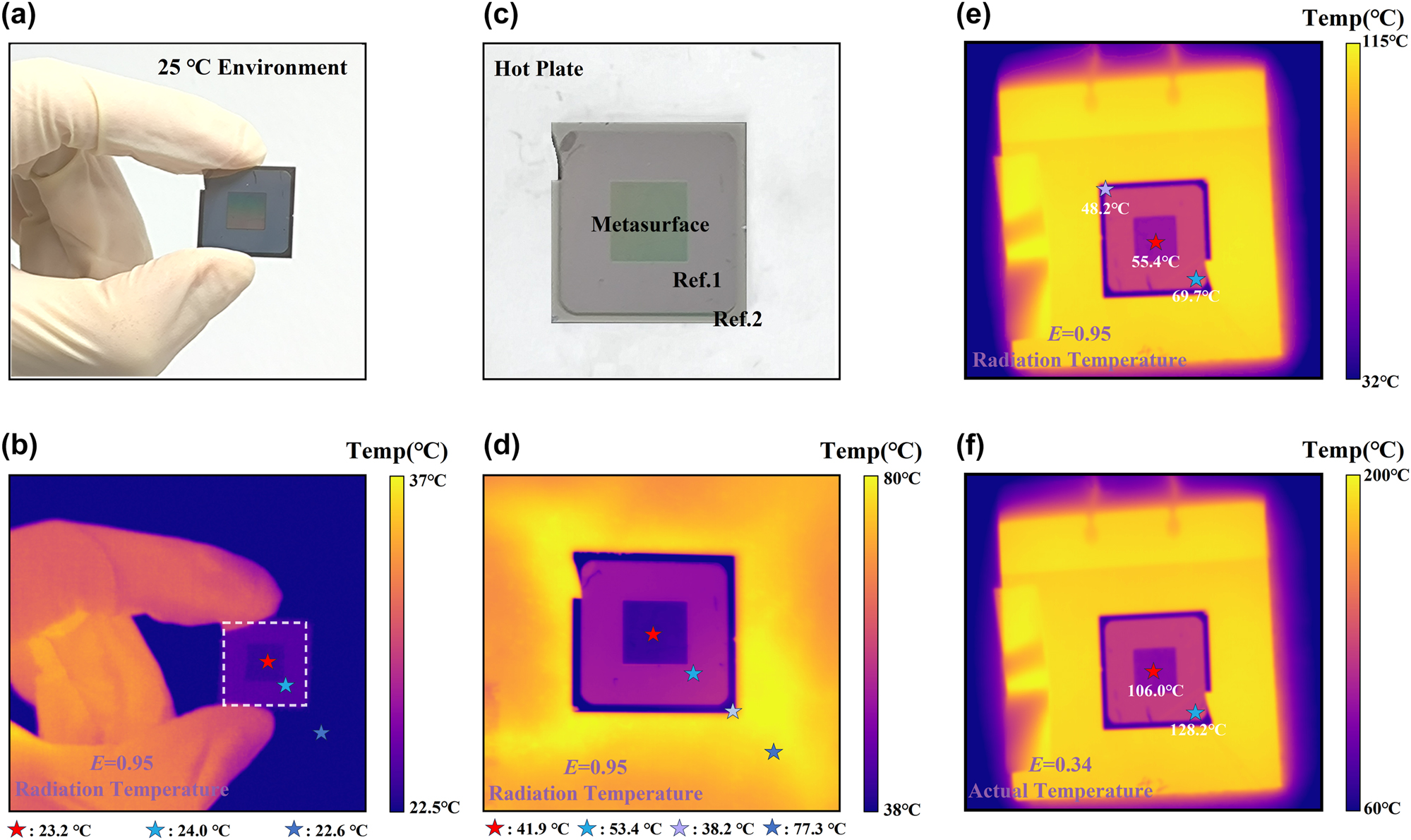
Optical image and IR radiation temperature distribution (metasurface: red, Ref. 1: sky blue, Ref. 2: purplish grey, background: blue). (a–b) The hand-held samples at room temperature represented the initial state. (c–d) Intermediate state. (e) Steady-state temperature distribution setting the in-camera emissivity to E = 0.95. (f) Steady-state temperature distribution setting the in-camera emissivity to E = 0.34.
3 Conclusions
In conclusion, we have developed an SMDM metasurface emitter, which is engineered to achieve high energy dissipation efficiency in the non-ATW, making it ideal for advanced infrared camouflage applications. Our SMDM metasurface utilizes semimetal Bi, which displays high positive values in the real part of the dielectric constant in the IR range, acting as a lossy dielectric medium. This configuration enables hybrid plasmonic resonances, resulting in effective broadband emission in the 5–8 μm non-ATW. Comparative experiments show that our metasurface can achieve up to a 25 °C reduction in radiative temperature compared to a sample lacking non-ATW energy dissipation capability (Ref. 1), highlighting its superior energy dissipation performance. Additionally, while the radiation temperature of our metasurface is slightly higher than a metal film (Ref. 2), it maintains a significantly lower actual temperature, demonstrating its good thermal stability. These findings offer a straightforward method for achieving broadband, high-efficiency emission in the non-ATW through strategic structural design, which benefits IR camouflage applications and suggests potential for wide deployment in IR technologies.
4 Materials and methods
4.1 Optical constants measurement
The optical constants of the deposited Bi film were measured and fitted in the infrared range using infrared spectroscopic ellipsometry (Sendira Sentech, 1,500–25,000 nm). This measurement accounts for a roughness layer of approximately 7 nm, while the optical constants of Ti and ZnS were obtained from the literature [53].
4.2 Electromagnetic simulation
The finite-difference time-domain (FDTD) method was utilized to simulate the reflectance and absorbance spectra and the electromagnetic field information inside the structure. The S-parameters were calculated by rigorous coupled wave analysis (RCWA).
4.3 Device fabrication
The SMDM metasurface emitter, Ref. 1, and Ref. 2 were prepared on the same wafer using electron-beam evaporation (Syskey Technology UHEB-LC6-03 system). Ti and ZnS were deposited at room temperature, with deposition rates of 2 A/s and 10 A/s, respectively. The metasurface array was patterned using laser lithography (SVG Microlab) with UV photoresist (AZ5214). A 25 nm layer of Bi was deposited at a rate of 2 A/s. After lift-off, an additional 153 nm thick layer of Bi was deposited, properly aligning Ref. 1 around the metasurface array.
4.4 Sample characterization
The micro-scale Fourier transform infrared spectrometer (Thermo Scientific Nicolet iN10) was used to obtain the different sizes of micro-area metasurface array reflectance spectra. The angle-resolved reflectance spectra over a range of 30°–70° were obtained using a Fourier transform infrared spectrometer (Thermo Scientific Nicolet iS50), both covering a spectral range of 8,000–400 cm−1. Additionally, the morphologies of the SMDM metasurface were characterized using a scanning electron microscope (FEI Sirion 200) with an accelerating voltage of 10 kV. Thermal measurements were conducted using an LWIR camera (Fotric 220) with a default emissivity of 0.95, operating in the 8–14 μm wavelength range. The AnalyzIR software package was used to extract radiation and actual temperature curves from LWIR images for the center (SMDM-S1) and peripheral (Ref. 1, Ref. 2) areas of the device. Heating power ranging from 0 to 10 W were applied using a DC power supply linked with a ceramic hotplate. The temperature trends over time for SMDM-S1, Ref. 1, and Ref. 2 were recorded using a 6 W heating power and the steady-state temperature of the hotplate is ∼135 °C measured by a thermocouple.
Funding source: National Key Research and Development Program of China
Award Identifier / Grant number: 2022YFA1404701
Funding source: Science and Technology Commission of Shanghai Municipality
Award Identifier / Grant number: 20JC1414603
Award Identifier / Grant number: 23ZR1473300
Award Identifier / Grant number: 23dz2260100
Funding source: National Natural Science Foundation of China
Award Identifier / Grant number: 11933006
Award Identifier / Grant number: 62075231
Award Identifier / Grant number: U2141240
Funding source: Shanghai Innovation Project
Award Identifier / Grant number: 2021-cyxt1-kj04
-
Research funding: This work was supported by the National Key R&D Program of China (2022YFA1404701), National Natural Science Foundation of China (62075231, 11933006, U2141240), Shanghai Science and Technology Committee (20JC1414603, 23dz2260100, 23ZR1473300), Shanghai Innovation Project (2021-cyxt1-kj04).
-
Author contributions: DZ: conceptualization, methodology, software, investigation, validation, formal analysis, visualization, writing – original draft. JZ: investigation, validation. CT: formal analysis, validation. LL: investigation, validation. QQ: investigation, validation. ZZ: investigation, validation. YS: resources, supervision. LZ: resources, supervision, funding acquisition. ND: resources, supervision, funding acquisition. JC: resources, supervision, funding acquisition. JH: conceptualization, methodology, validation, formal analysis, writing – review & editing, resources, supervision, project administration, funding acquisition. All authors have accepted responsibility for the entire content of this manuscript and approved its submission.
-
Conflict of interest: Authors state no conflicts of interest.
-
Data availability: All data are available in the main text or the Supplementary Materials. Requests should be directed to the corresponding author.
References
[1] R. Hu, et al.., “Thermal camouflaging metamaterials,” Mater. Today, vol. 45, pp. 120–141, 2021. https://doi.org/10.1016/j.mattod.2020.11.013.Search in Google Scholar
[2] Y. Wu, S. Tan, Y. Zhao, L. Liang, M. Zhou, and G. Ji, “Broadband multispectral compatible absorbers for radar, infrared and visible stealth application,” Prog. Mater. Sci., vol. 135, 2023, Art. no. 101088. https://doi.org/10.1016/j.pmatsci.2023.101088.Search in Google Scholar
[3] J. Teyssier, S. V. Saenko, D. Van Der Marel, and M. C. Milinkovitch, “Photonic crystals cause active colour change in chameleons,” Nat. Commun., vol. 6, no. 1, p. 6368, 2015. https://doi.org/10.1038/ncomms7368.Search in Google Scholar PubMed PubMed Central
[4] G. M. Akselrod, et al.., “Large‐area metasurface perfect absorbers from visible to near‐infrared,” Adv. Mater., vol. 27, no. 48, pp. 8028–8034, 2015. https://doi.org/10.1002/adma.201503281.Search in Google Scholar PubMed
[5] S. Chandra, D. Franklin, J. Cozart, A. Safaei, and D. Chanda, “Adaptive multispectral infrared camouflage,” ACS Photonics, vol. 5, no. 11, pp. 4513–4519, 2018. https://doi.org/10.1021/acsphotonics.8b00972.Search in Google Scholar
[6] Y. Jia, et al.., “Transparent dynamic infrared emissivity regulators,” Nat. Commun., vol. 14, no. 1, p. 5087, 2023. https://doi.org/10.1038/s41467-023-40902-w.Search in Google Scholar PubMed PubMed Central
[7] T. Kim, J. Bae, N. Lee, and H. H. Cho, “Hierarchical metamaterials for multispectral camouflage of infrared and microwaves,” Adv. Funct. Mater., vol. 29, no. 10, 2019, Art. no. 1807319. https://doi.org/10.1002/adfm.201807319.Search in Google Scholar
[8] W. Wang, et al.., “Broadband radar-absorbing performance of square-hole structure,” Adv. Compos. Hybrid Mater., vol. 5, no. 1, pp. 525–535, 2022. https://doi.org/10.1007/s42114-021-00376-0.Search in Google Scholar
[9] M. Dirnwoeber, R. Machan, and J. Herler, “Coral reef surveillance: infrared-sensitive video surveillance Technology as a new tool for diurnal and nocturnal long-term field observations,” Remote Sens., vol. 4, no. 11, pp. 3346–3362, 2012. https://doi.org/10.3390/rs4113346.Search in Google Scholar PubMed PubMed Central
[10] J. Zhang, R. Wei, M. ElKabbash, E. M. Campbell, and C. Guo, “Thin-film perfect infrared absorbers over single- and dual-band atmospheric windows,” Opt. Lett., vol. 45, no. 10, p. 2800, 2020. https://doi.org/10.1364/OL.392651.Search in Google Scholar PubMed
[11] S. Zhou, et al.., “Continuous programmable mid-infrared thermal emitter and camouflage based on the phase-change material In3 SbTe2,” Opt. Lett., vol. 48, no. 16, p. 4388, 2023. https://doi.org/10/g7m3r6.10.1364/OL.497404Search in Google Scholar PubMed
[12] Y. Qu, et al.., “Thermal camouflage based on the phase-changing material GST,” Light: Sci. Appl., vol. 7, no. 1, p. 26, 2018. https://doi.org/10.1038/s41377-018-0038-5.Search in Google Scholar PubMed PubMed Central
[13] J. Kim, C. Park, and J. W. Hahn, “Metal–semiconductor–metal metasurface for multiband infrared stealth Technology using camouflage color pattern in visible range,” Adv. Opt. Mater., vol. 10, no. 6, 2022, Art. no. 2101930. https://doi.org/10.1002/adom.202101930.Search in Google Scholar
[14] M. Li, D. Liu, H. Cheng, L. Peng, and M. Zu, “Manipulating metals for adaptive thermal camouflage,” Sci. Adv., vol. 6, no. 22, 2020. https://doi.org/10.1126/sciadv.aba3494.Search in Google Scholar PubMed PubMed Central
[15] J. Chen, X. Liu, P. Wang, C. Xiao, S. Chen, and H. Zhou, “Epsilon-near-zero material-based bi-layer metamaterials for selective mid-infrared radiation,” Nanotechnology, vol. 35, no. 5, 2024, Art. no. 055302. https://doi.org/10.1088/1361-6528/ad074f.Search in Google Scholar PubMed
[16] J. Zhou, Z. Zhan, F. Zhu, and Y. Han, “Preparation of flexible wavelength-selective metasurface for infrared radiation regulation,” ACS Appl. Mater. Interfaces, vol. 15, no. 17, pp. 21629–21639, 2023. https://doi.org/10.1021/acsami.3c01452.Search in Google Scholar PubMed
[17] D. Ding, X. He, S. Liang, W. Wei, and S. Ding, “Porous nanostructured composite film for visible-to-infrared camouflage with thermal management,” ACS Appl. Mater. Interfaces, vol. 14, no. 21, pp. 24690–24696, 2022. https://doi.org/10.1021/acsami.2c03509.Search in Google Scholar PubMed
[18] M. Pan, et al.., “Multi-band middle-infrared-compatible camouflage with thermal management via simple photonic structures,” Nano Energy, vol. 69, 2020, Art. no. 104449. https://doi.org/10.1016/j.nanoen.2020.104449.Search in Google Scholar
[19] N. Lee, T. Kim, J.-S. Lim, I. Chang, and H. H. Cho, “Metamaterial-selective emitter for maximizing infrared camouflage performance with energy dissipation,” ACS Appl. Mater. Interfaces, vol. 11, no. 23, pp. 21250–21257, 2019. https://doi.org/10.1021/acsami.9b04478.Search in Google Scholar PubMed
[20] K. Yu, W. Zhang, M. Qian, P. Shen, and Y. Liu, “Multiband metamaterial emitters for infrared and laser compatible stealth with thermal management based on dissipative dielectrics,” Photonics Res., vol. 11, no. 2, p. 290, 2023. https://doi.org/10.1364/PRJ.476109.Search in Google Scholar
[21] N. Lee, J.-S. Lim, J. Nam, H. M. Bae, and H. H. Cho, “Durable camouflage materials by polyimide nanofilm with thermal management,” Appl. Surf. Sci., vol. 608, 2023, Art. no. 155107. https://doi.org/10.1016/j.apsusc.2022.155107.Search in Google Scholar
[22] N. Lee, et al.., “Multiple resonance metamaterial emitter for deception of infrared emission with enhanced energy dissipation,” ACS Appl. Mater. Interfaces, vol. 12, no. 7, pp. 8862–8869, 2020. https://doi.org/10.1021/acsami.9b21030.Search in Google Scholar PubMed
[23] L. Peng, D. Liu, H. Cheng, S. Zhou, and M. Zu, “A multilayer film based selective thermal emitter for infrared stealth Technology,” Adv. Opt. Mater., vol. 6, no. 23, 2018, Art. no. 1801006. https://doi.org/10.1002/adom.201801006.Search in Google Scholar
[24] X. Jiang, et al.., “Implementing of infrared camouflage with thermal management based on inverse design and hierarchical metamaterial,” Nanophotonics, vol. 12, no. 10, pp. 1891–1902, 2023. https://doi.org/10.1515/nanoph-2023-0067.Search in Google Scholar PubMed PubMed Central
[25] L. Wang, et al.., “Combined multi-band infrared camouflage and thermal management via a simple multilayer structure design,” Opt. Lett., vol. 46, no. 20, p. 5224, 2021. https://doi.org/10.1364/OL.441605.Search in Google Scholar PubMed
[26] H. Zhu, et al.., “Multispectral camouflage for infrared, visible, lasers and microwave with radiative cooling,” Nat. Commun., vol. 12, no. 1, p. 1805, 2021. https://doi.org/10.1038/s41467-021-22051-0.Search in Google Scholar PubMed PubMed Central
[27] L. Huang, et al.., “Multiband camouflage design with thermal management,” Photonics Res., vol. 11, no. 5, p. 839, 2023. https://doi.org/10.1364/PRJ.484448.Search in Google Scholar
[28] Z. Ren, et al.., “Infrared camouflage based on the crystalline and amorphous GST multilayer films,” Appl. Phys. Lett., vol. 121, no. 25, p. 253504, 2023. https://doi.org/10.1063/5.0134673.Search in Google Scholar
[29] M. Han, et al.., “Versatility of infrared properties of MXenes,” Mater. Today, vol. 45, pp. 31–39, 2023. https://doi.org/10.1016/j.mattod.2023.02.024.Search in Google Scholar
[30] C. Chen, et al.., “Large-area long-wave infrared broadband all-dielectric metasurface absorber based on maskless laser direct writing lithography,” Opt. Express, vol. 30, no. 8, 2022, Art. no. 13391. https://doi.org/10.1364/oe.447783.Search in Google Scholar
[31] Z. Deng, Y. Su, W. Qin, T. Wang, X. Wang, and R. Gong, “Nanostructured Ge/ZnS films for multispectral camouflage with low visibility and low thermal emission,” ACS Appl. Nano Mater., vol. 5, no. 4, pp. 5119–5127, 2022. https://doi.org/10.1021/acsanm.2c00088.Search in Google Scholar
[32] S. Dang and H. Ye, “A visible-infrared-compatible camouflage photonic crystal with heat dissipation by radiation in 5–8 μm,” Cell Rep. Phys. Sci., vol. 2, no. 11, 2021, Art. no. 100617. https://doi.org/10.1016/j.xcrp.2021.100617.Search in Google Scholar
[33] J. Zhang, et al.., “Long-wavelength infrared selective emitter for thermal infrared camouflage under a hot environment,” Opt. Express, vol. 30, no. 13, 2022, Art. no. 24132. https://doi.org/10.1364/OE.462166.Search in Google Scholar PubMed
[34] J. Hao, J. Wang, X. Liu, W. J. Padilla, L. Zhou, and M. Qiu, “High performance optical absorber based on a plasmonic metamaterial,” Appl. Phys. Lett., vol. 96, no. 25, 2010, Art. no. 251104. https://doi.org/10.1063/1.3442904.Search in Google Scholar
[35] J. Hao, L. Zhou, and M. Qiu, “Nearly total absorption of light and heat generation by plasmonic metamaterials,” Phys. Rev. B, vol. 83, no. 16, 2011, Art. no. 165107. https://doi.org/10.1103/PhysRevB.83.165107.Search in Google Scholar
[36] W. Yu, et al.., “Large‐area, broadband, wide‐angle plasmonic metasurface absorber for midwavelength infrared atmospheric transparency window,” Adv. Opt. Mater., vol. 7, no. 20, 2019, Art. no. 1900841. https://doi.org/10.1002/adom.201900841.Search in Google Scholar
[37] X. Pan, et al.., “Spatial and frequency selective plasmonic metasurface for long wavelength infrared spectral region,” Adv. Opt. Mater., vol. 6, no. 20, 2018, Art. no. 1800337. https://doi.org/10.1002/adom.201800337.Search in Google Scholar
[38] D. Rodrigo, A. Tittl, A. John-Herpin, O. Limaj, and H. Altug, “Self-similar multiresonant nanoantenna arrays for sensing from near- to mid-infrared,” ACS Photonics, vol. 5, no. 12, pp. 4903–4911, 2018. https://doi.org/10.1021/acsphotonics.8b01050.Search in Google Scholar
[39] C. Li, et al.., “Near-field and far-field thermal emission of an individual patch nanoantenna,” Phys. Rev. Lett., vol. 121, no. 24, 2018, Art. no. 243901. https://doi.org/10.1103/PhysRevLett.121.243901.Search in Google Scholar PubMed
[40] A. Ghobadi, H. Hajian, M. Gokbayrak, B. Butun, and E. Ozbay, “Bismuth-based metamaterials: from narrowband reflective color filter to extremely broadband near perfect absorber,” Nanophotonics, vol. 8, no. 5, pp. 823–832, 2019. https://doi.org/10.1515/nanoph-2018-0217.Search in Google Scholar
[41] F. Chacon‐Sanchez, et al.., “Building conventional metasurfaces with unconventional interband plasmonics: a versatile route for sustainable structural color generation based on bismuth,” Adv. Opt. Mater., vol. 12, no. 10, 2024, Art. no. 2302130. https://doi.org/10.1002/adom.202302130.Search in Google Scholar
[42] Q. Xu, et al.., “Ultra-thin midwavelength infrared absorber using bismuth based planar thin film metamaterials,” Appl. Phys. Express, vol. 15, no. 8, 2022, Art. no. 082005. https://doi.org/10.35848/1882-0786/ac8415.Search in Google Scholar
[43] C. Tan, et al.., “Deep-subwavelength multilayered meta-coatings for visible-infrared compatible camouflage,” Nanophotonics, vol. 13, no. 13, pp. 2391–2400, 2024. https://doi.org/10.1515/nanoph-2024-0029.Search in Google Scholar PubMed PubMed Central
[44] D. Lee, et al.., “Hyperbolic metamaterials: fusing artificial structures to natural 2D materials,” eLight, vol. 2, no. 1, p. 1, 2022. https://doi.org/10.1186/s43593-021-00008-6.Search in Google Scholar
[45] S. Zhou, S. Dong, Y. Guo, Y. Shuai, H.-X. Xu, and G. Hu, “Colored thermal camouflage and anti-counterfeiting with programmable In3 SbTe2 platform,” Nanophotonics, vol. 13, no. 6, pp. 945–954, 2024. https://doi.org/10.1515/nanoph-2023-0924.Search in Google Scholar PubMed PubMed Central
[46] X. Wang, et al.., “Advances in information processing and biological imaging using flat optics,” Nat. Rev. Electr. Eng., vol. 1, no. 6, pp. 391–411, 2024. https://doi.org/10.1038/s44287-024-00057-2.Search in Google Scholar
[47] M. A. Kats, R. Blanchard, P. Genevet, and F. Capasso, “Nanometre optical coatings based on strong interference effects in highly absorbing media,” Nat. Mater., vol. 12, no. 1, pp. 20–24, 2013. https://doi.org/10.1038/nmat3443.Search in Google Scholar PubMed
[48] H. Pan, et al.., “Wide gamut, angle-insensitive structural colors based on deep-subwavelength bilayer media,” Nanophotonics, vol. 9, no. 10, pp. 3385–3392, 2020. https://doi.org/10.1515/nanoph-2020-0106.Search in Google Scholar
[49] Z. Zhang, et al.., “Ultra-thin optical power converters based on Gires–Tournois resonator configuration operating in high-order modes,” Appl. Phys. Express, vol. 17, no. 7, 2024, Art. no. 072002. https://doi.org/10.35848/1882-0786/ad59f5.Search in Google Scholar
[50] W. Zhao, et al.., “Remarkable photoluminescence enhancement of CsPbBr 3 perovskite quantum dots assisted by metallic thin films,” Nanophotonics, vol. 10, no. 8, pp. 2257–2264, 2021. https://doi.org/10.1515/nanoph-2021-0064.Search in Google Scholar
[51] M. A. Kats and F. Capasso, “Optical absorbers based on strong interference in ultra‐thin films,” Laser Photonics Rev., vol. 10, no. 5, pp. 735–749, 2016. https://doi.org/10.1002/lpor.201600098.Search in Google Scholar
[52] J. Toudert, R. Serna, M. G. Pardo, N. Ramos, R. J. Peláez, and B. Maté, “Mid-to-far infrared tunable perfect absorption by a sub - λ/100 nanofilm in a fractal phasor resonant cavity,” Opt. Express, vol. 26, no. 26, 2018, Art. no. 34043. https://doi.org/10.1364/OE.26.034043.Search in Google Scholar PubMed
[53] E. D. Palik, Handbook of Optical Constants of Solids, San Diego, Academic Press, 1998.Search in Google Scholar
Supplementary Material
This article contains supplementary material (https://doi.org/10.1515/nanoph-2024-0538).
© 2025 the author(s), published by De Gruyter, Berlin/Boston
This work is licensed under the Creative Commons Attribution 4.0 International License.
Articles in the same Issue
- Frontmatter
- Editorial
- Special issue: “Metamaterials and Plasmonics in Asia”
- Reviews
- All-optical analog differential operation and information processing empowered by meta-devices
- Metasurface-enhanced biomedical spectroscopy
- Topological guided-mode resonances: basic theory, experiments, and applications
- Letter
- Ultrasensitive circular dichroism spectroscopy based on coupled quasi-bound states in the continuum
- Research Articles
- Data-efficient prediction of OLED optical properties enabled by transfer learning
- Semimetal–dielectric–metal metasurface for infrared camouflage with high-performance energy dissipation in non-atmospheric transparency window
- Deep-subwavelength engineering of stealthy hyperuniformity
- Tunable structural colors based on grayscale lithography and conformal coating of VO2
- A general recipe to observe non-Abelian gauge field in metamaterials
- Free-form catenary-inspired meta-couplers for ultra-high or broadband vertical coupling
- Enhanced photoluminescence of strongly coupled single molecule-plasmonic nanocavity: analysis of spectral modifications using nonlocal response theory
- Spectral Hadamard microscopy with metasurface-based patterned illumination
- Tunneling of two-dimensional surface polaritons through plasmonic nanoplates on atomically thin crystals
- Highly sensitive microdisk laser sensor for refractive index sensing via periodic meta-hole patterning
- Scaled transverse translation by planar optical elements for sub-pixel sampling and remote super-resolution imaging
- Hyperbolic polariton-coupled emission optical microscopy
- Broadband perfect Littrow diffraction metasurface under large-angle incidence
- Role of complex energy and momentum in open cavity resonances
- Are nanophotonic intermediate mirrors really effective in enhancing the efficiency of perovskite tandem solar cells?
- Tunable meta-device for large depth of field quantitative phase imaging
- Enhanced terahertz magneto-plasmonic effect enabled by epsilon-near-zero iron slot antennas
- Baseline-free structured light 3D imaging using a metasurface double-helix dot projector
- Nanophotonic device design based on large language models: multilayer and metasurface examples
- High-efficiency generation of bi-functional holography with metasurfaces
- Dielectric metasurfaces based on a phase singularity in the region of high reflectance
- Exceptional points in a passive strip waveguide