Ultrafast acousto-optic modulation at the near-infrared spectral range by interlayer vibrations
-
Tae Gwan Park
 ,
Chaeyoon Kim
,
Chaeyoon Kim


Abstract
The acousto-optic modulation over a broad near-infrared (NIR) spectrum with high speed, excellent integrability, and relatively simple scheme is crucial for the application of next-generation opto-electronic and photonic devices. This study aims to experimentally demonstrate ultrafast acousto-optic phenomena in the broad NIR spectral range of 0.77–1.1 eV (1130–1610 nm). Hundreds of GHz of light modulation are revealed in an all-optical configuration by combining ultrafast optical spectroscopy and light–sound conversion in 10–20 nm-thick bismuth selenide (Bi2Se3) van der Waals thin films. The modified optical transition energy and the line shape in the NIR band indicate phonon–photon interactions, resulting in a modulation of optical characteristics by the photoexcited interlayer vibrations in Bi2Se3. This all-optical, ultrafast acousto-optic modulation approach may open avenues for next-generation nanophotonic applications, including optical communications and processing, due to the synergistic combination of large-area capability, high photo-responsivity, and frequency tunability in the NIR spectral range.
1 Introduction
Light modulation in terms of amplitude, frequency, momentum, and polarization is crucial for signal processing and telecommunication in optoelectronic and photonics fields. A key method for achieving this modulation is acousto-optic (AO) modulation, which relies on the coupling of phonons and photons, causing optical constants to fluctuate due to acoustic waves in materials. Phonon–photon coupling forms the basis for commercial AO devices [1] and recent amplitude/phase modulators [2], tweezers [3], beam steering [4], nonreciprocal light propagation [5], [6], active information manipulation [7], and spatial mode conversion [8]. Conventional AO devices are typically centimeter-scale in size, employing bulk crystals and operating in the MHz range. Despite their excellent performance, current AO devices encounter challenges in compatibility with high-speed modulation in the GHz to THz range and emerging integrated on-chip systems [9], [10]. Despite achieving high-frequency modulations with integrability at a small scale, the determination of operating wavelengths requires a comprehensive study of optomechanics. For instance, investigations such as generating high-intensity phonons with the large modal overlap of acousto-optic coupling are required.
One of the most straightforward methods for this purpose is optical spectroscopy, including measurement techniques such as absorption, reflectivity, and photoluminescence during acoustic interactions [11]. However, this method lacks details regarding modulation speed, phase, and the specific phonon modes involved in the operation. An alternative approach is ultrafast optical approach, allowing the observation of phonon–photon interactions in both time and energy domains [12], [13], [14]. Ultrashort pump pulses generate acoustic waves on the material surface and inside it by increasing carrier density and lattice temperature [15]. Subsequent broadband probe pulses are then utilized to monitor the modulation of optical properties resulting from AO effects. This study on ultrafast acousto-optic modulation reveals temporal and simultaneous spectroscopic features, including operating speed, decoherence time, and modifications in optical properties through acoustic modulation of particular phonon modes.
We aim to develop a high-speed AO modulator that operates at near-infrared (NIR) wavelengths, similar to those commonly used in modern communication, capable of achieving speeds in the hundreds of GHz. We employ ultrafast optical spectroscopy with a broadband NIR probe to introduce the ultrafast light modulation via a AO coupling in bismuth selenide (Bi2Se3) van der Waals (vdW) thin films. The ultrafast pump pulses generate out-of-plane strain and interlayer vibrations as shown in Figure 1(a). A broadband NIR probe light (0.77–1.1 eV) is then applied to detect AO modulations. Our results demonstrate that changes in interlayer distance cause fluctuations in optical properties. The shift of interband transition energy at approximately 15 meV and the line shape change at 40 meV are observed through the AO effects in the NIR band. The experimental results are reproduced well by the strain-dependent density functional theory (DFT) calculations, which facilitated electronic band modulation, including energy and curvature by lattice deformation. Within the vdW gap oscillations, the modulation frequency can widely be tuned from a few GHz to sub-THz. Our findings prove the feasibility of the presented all-optical AO modulation by exploiting Bi2Se3 thin films for light modulator at NIR wavelengths with high speed and integrability in on-chip and nano-devices.
![Figure 1:
(a) Crystal structure of Bi2Se3-layered vdW thin films and interlayer modulation schematic by out-of-plane straining and (b) real (n) and imaginary part (κ) of refractive index of Bi2Se3 obtained from [16]. The pump and probe photon energies used here are indicated by the vertical arrow and the gray area, respectively.](/document/doi/10.1515/nanoph-2023-0769/asset/graphic/j_nanoph-2023-0769_fig_001.jpg)
(a) Crystal structure of Bi2Se3-layered vdW thin films and interlayer modulation schematic by out-of-plane straining and (b) real (n) and imaginary part (κ) of refractive index of Bi2Se3 obtained from [16]. The pump and probe photon energies used here are indicated by the vertical arrow and the gray area, respectively.
2 Results and discussion
In this study, high-quality Bi2Se3 vdW thin films were prepared by molecular beam epitaxy with different thicknesses on an Al2O3 (0001) substrate. The crystal structures of Bi2Se3 are rhombohedral layered structure with a unit quintuple layer (QL) (see Figure 1(a)). The QL corresponds to a thickness of 1 nm. Atomic force microscopy confirmed the number of QLs in the used sample as 13, 17, and 22 QLs. Figure 1(b) shows the real (n) and imaginary (κ) part of the refractive index of the Bi2Se3 films at the ground state, as obtained from recent spectroscopic ellipsometry for the 10-QL Bi2Se3 by Fang [16]. At the NIR range, the κ values became significant from 0.9 eV, indicating an absorption edge. A broad peak near 1.0 eV featured a resonant interband transition within the continuum free carriers. The peak energy near 1.0 eV was consistent with the interband transition in NIR band [16], [17].
We investigated ultrafast acousto-optic effects through transient reflectivity (TR) spectroscopy, employing a NIR pump and widely tunable NIR probe pulses. To generate these pulses, we used an 80-MHz Ti:sapphire oscillator (MAITAI, Spectra Physics) producing optical pulses with a photon energy of 1.5 eV and a pulse duration of 100 fs. This oscillator served as the pump for a synchronously pumped optical parametric oscillator (SPOPO) to generate tunable NIR probe pulses ranging from 0.77 to 1.1 eV. Approximately 60 % of the laser output power was used to pump the SPOPO, while the remaining power was used for optical pump pulses. These pump pulses excited carriers, leading to subsequent acoustic waves in van der Waals (vdW) thin films. The probe pulses were collinearly combined with the pump pulses using a dichroic mirror. The pump and probe beams were then focused on by the NIR objectives (Mitutoyo Apochromatic, 50× magnification). The pump fluence used in this work was approximately 120 μJ/cm2, yielding an excited carrier density (n ex ) of 5.8 × 1019 cm−3. By comparison, the probe fluence remained to be 102 times weaker than the pump fluence. The time delay was controlled using a linear translation stage. While tuning the probe wavelengths, we measured the TR (ΔR/R 0) signal with a free-space biased Ge detector (DET50B, Thorlabs) and a lock-in amplifier (SR830, Stanford Research System), chopping the optical pulses at 290 Hz. Spectral filters that acted as long-pass filters were used to block the pump beam in the photodetector. All ultrafast spectroscopic measurements were performed at room temperature and normal pressure. We obtained the transient NIR spectra due to the wide tuning range of the probe wavelength from SPOPO.
Figure 2(a) presents the TR signal for the 13-, 17-, and 22-QL Bi2Se3 films as a function of time and energy. The observed photocarrier dynamics extended over a nanosecond time frame. Figure 2(b) highlights the ultrafast response within 100 ps. Across all samples, three main features were noted: (1) initially, a negative TR was observed for all probe energies following photoexcitation. (2) Subsequently, a derivative-like differential spectrum, with a sign that changed depending on the energy due to resonant changes in optical transition, was subsequently obtained. (3) A noticeable sinusoidal modulation appeared within the incoherent background from the excited carriers.
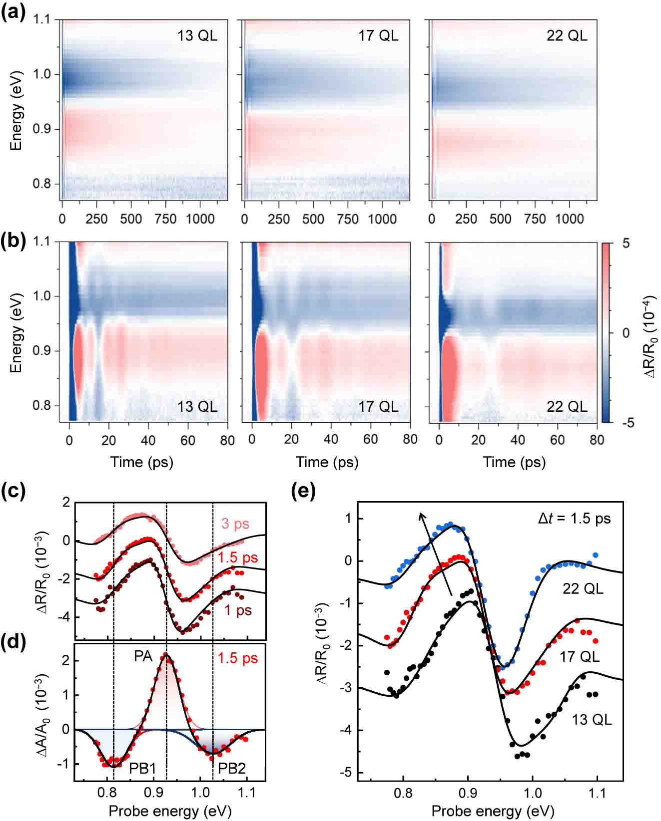
Ultrafast pump–probe spectroscopic results: (a) TR signals as a function of time and probe energy for the 13, 17, and 22 QL Bi2Se3 samples; (b) same TR signals in the (a) in short time window, which highlights spectral modulation by coherent oscillations. (c) Selected TR spectra in the 17-QL sample at 1, 1.5, and 3 ps time delay between pump and probe pulses; (d) corresponding TA spectra obtained using the Kramers–Kronig transformation; and (e) number of QLs-dependent TR spectra at 1.5 ps time delay, in which the black curves in (c–e) denote the fitting results based on the derivative-like response in the TA spectra and their Hilbert transformation result in TR spectra.
Figure 2(c) shows the TR spectra at selected time delays. The derivative-like signal was embedded within a negative ΔR/R 0 response across the entire energy range, persisting for 3 ps. Besides the negative TR response, the derivative-like TR feature also referred to the resonant changes in absorption derived by the Kramers–Kronig relation. We transformed the TR to the corresponding transient absorption (TA, ΔA/A 0) spectra using an inverse Hilbert transformation (iHT) as shown in Figure 2(d). The obtained TA displayed second derivative-like spectra with a central peak of the photo-induced absorption (PA) at 0.93 eV and two satellite peaks denoted as two photobleaching (PB) peaks at 0.82 and 1.03 eV. These observed TA spectra were linked to energy shifts and broadening associated with band filling during resonant transitions. The measured peak energy of the TA spectra was consistent with the interband transition energy in the equilibrium optical spectrum [16], [17]. From the thickness-dependent TR spectra in Figure 2(e), we observed a more pronounced negative in the ΔR/R 0 spectra in the thinner film. The characteristic spectra were redshifted according to the thickness increase. This behavior was consistent with a previous observation of the redshift in the optical transition energy as the sample thickness increased [16], [18].
Figure 3(a) shows the time-dependent changes of resonant energies, obtained from the TR spectra and the corresponding TA spectra. The transient spectrum features indicated the ultrafast nonequilibrium dynamics during 5 ps and slow recovery. Temporal traces at three representative peaks showed a bi-exponential decay and a coherent modulation, as illustrated in Figure 3(b). The PA signal amplitude was predominant. The signal amplitudes of the two satellite PB peaks were similar. The two decay times (τ 1 and τ 2) significantly differed at the ps and ns levels. The τ 1 timescale shows a good agreement with the previously reported decay constant (∼2–3.5 ps) explained by the electron–longitudinal optical phonon scattering [19], [20]. After the fast decay (τ 1), coherent modulation was observed, maintained for approximately 100 ps. The subsequent quasi-static state by the slow τ 2 provided optical modulation without background from electron dynamics. Figure 3(c) depicts the QL number-dependent photocarrier dynamics. The faster relaxation time was similar for all samples. By contrast, the slower τ 2 became slower as its thickness increased. Each decay time was obtained by fitting with the bi-exponential decay functions (Figure 3(d)). Note that the characteristics of the decay constants of PA and PB were almost the same. In other words, the observed changes in the NIR spectrum were caused by the excited electrons in conduction band and the subsequent line shape changes, which induced a second derivative-like TR signal.
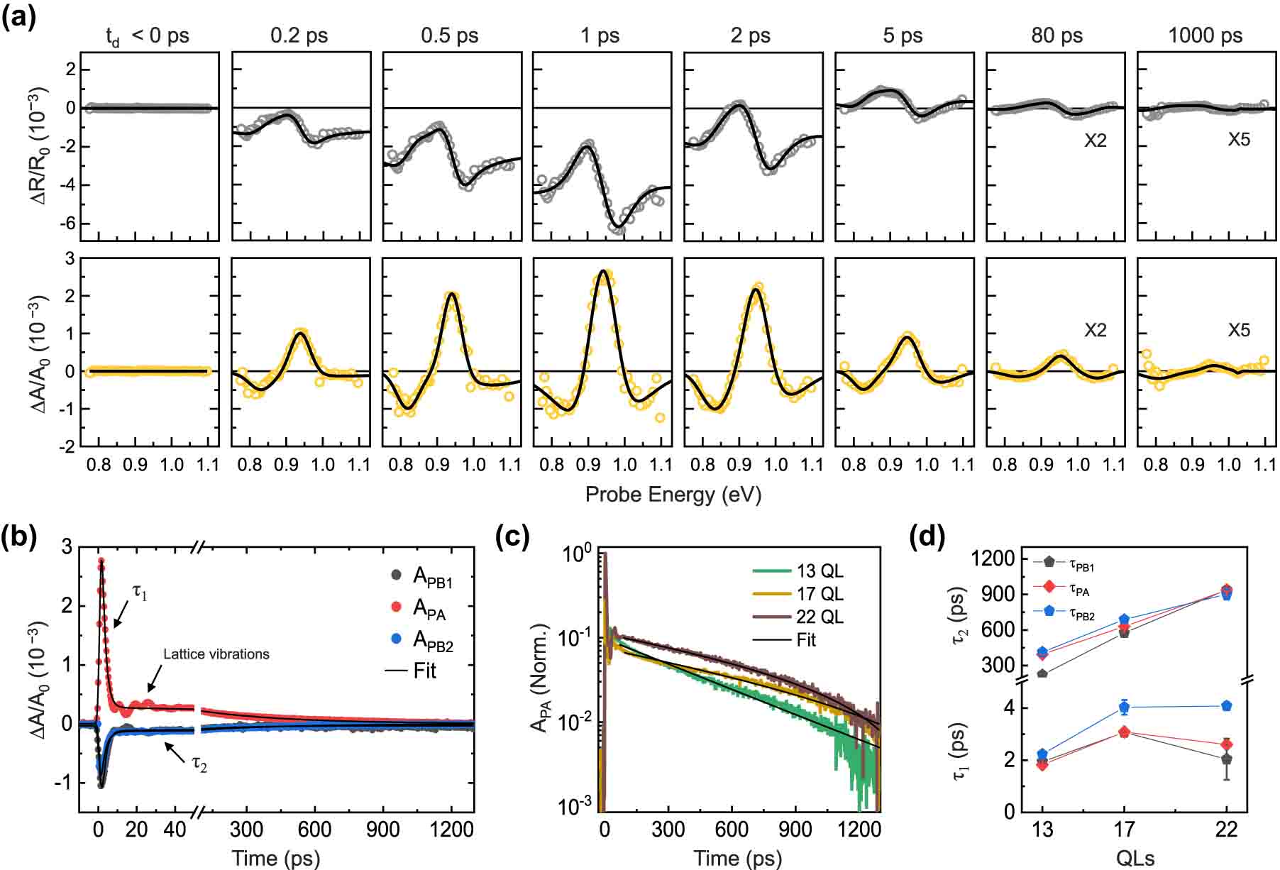
Ultrafast carrier dynamics: (a) time-dependent TR spectra and corresponding TA spectra, with black curves representing fitting results based on the Kramers–Kronig relation. (b) Pump–probe traces collected at resonant energies (PB1 and 2 and PA); (c) relaxation dynamics of excited carriers dependent on the number of QLs, with black curves indicating fitting based on the bi-exponential decay function; and (d) decay constant obtained from (c).
While the excited carriers persisted, a robust sinusoidal modulation with temporal coherence extending beyond 100 ps was observed. In Figure 4(a) and (b), representative transient reflectivity (TR) spectra and corresponding transient absorption (TA) spectra from the 17-QL sample at the selected time delay are depicted, highlighting the modulation’s maximum/minimum. Starting from 15 ps, reflectivity and absorption were significantly suppressed at 20 ps in the full probe range. The TR/TA spectra were subsequently recovered at 25 ps. The resonant energy was shifted (ΔE) through acoustic modulation. In Figure 4(b), the energy difference between the two satellite PB peaks (E PB1–E PB2) was reduced at 20 ps and recovered when compared to the spectra at 15 and 25 ps. For the second derivative TA, the E PB1–E PB2 reduction indicated the narrowing of the resonant optical transition by the ultrafast acoustic modulation. We visualized the ultrafast energy modulation of the interband transition by tracking the peak positions of the PB/PA in the TA spectra as shown in Figure 4(c).
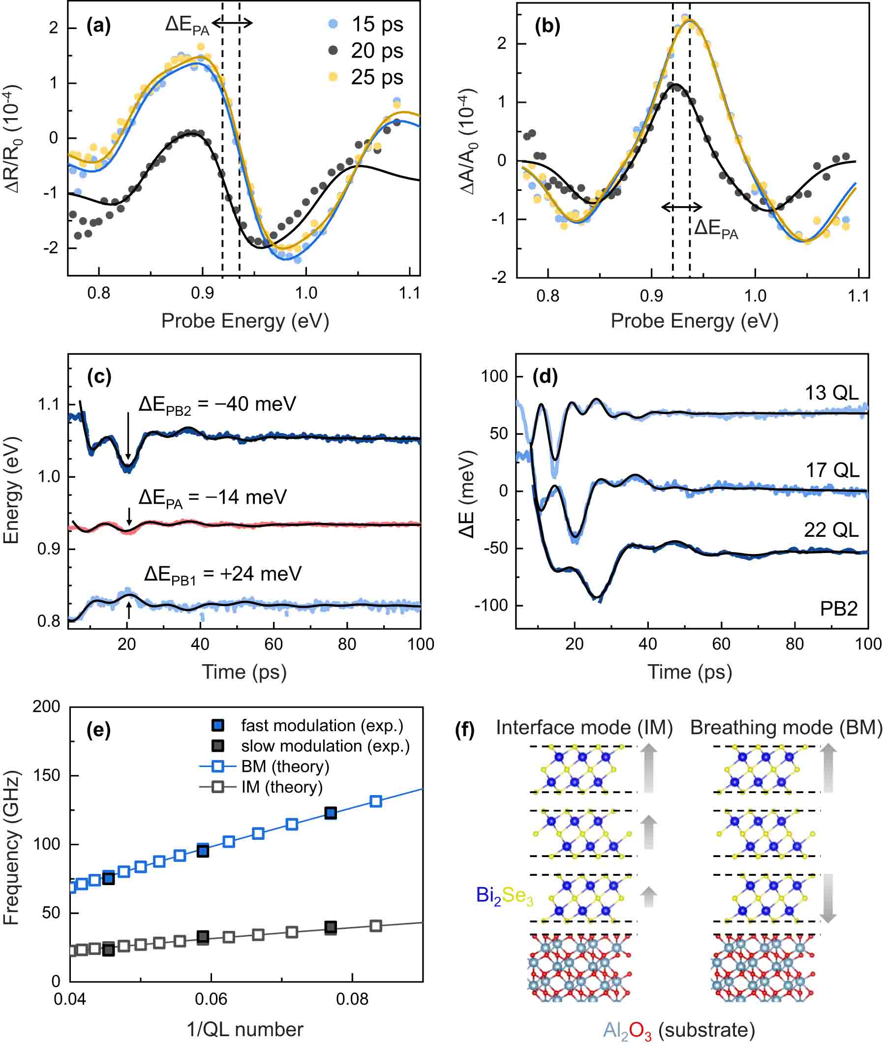
Ultrafast acousto-optic modulation: (a) representative TR spectra and (b) corresponding TA spectra at maximum and minimum modulations; (c) temporal traces of the resonant energy modulation for three resonant peaks; (d) time and number of QLs-dependent energy modulation for PB2 peak; (e) observed QL-dependent modulation frequency and simulation results based on the linear chain model with substrate effects; and (f) schematic of the layer vibrational modes measured through TR spectroscopy.
The energy variation reached a maximum around 20 ps and was damped after three periods. In the 100 ps window in Figure 4(c), the TA spectra characteristics were quasi-static, that is, flat over the time window. To assess the energy difference caused by acoustic effects, we referenced the peak energies at 100 ps. The reductions in energy for the PB2 and PA bands were 40 and 14 meV, respectively, while the PB1 energy increased by 24 meV. Considering the second derivative-like TA spectra, the asymmetrical shift of the three peak energies can be interpreted by the shift and the broadening of the optical transition. The opposite sign of the energy variation for the PB1 and PB2 bands indicated the resonance narrowing, which implied the electronic band shrinkage. The asymmetric shifts between the PB1 and PB2 bands indicate energy gap change of the central resonant energy. This was also inferred from the fact that the energy variation asymmetry in the PB bands was similar to the shift value of the PA peak (i.e., ΔE PB1 + ΔE PB2 ∼ ΔE PA). Consequently, the ultrafast light-induced acoustic effects can shift and shrink the electronic band. Figure 4(d) illustrates the QL number-dependent ultrafast response of the resonant energy. The PB2 band was suitable for clearly comparing the number of QLs-dependent modulation speeds due to the largest amplitude of the energy modulation. Thicker samples showed more significant energy changes induced by vibration. The time-varying signal was well-fitted with two damped oscillations, and the fast and slow modulation components strongly depended on the QL number.
Figure 4(e) presents the frequencies obtained according to the QLs. The number of QLs dependent frequency in the layered system implied the unique interlayer vibrational modes caused by the weak vdW interactions explained by the linear chain model [21], [22], [23], [24], [25]. We calculated the frequency (f) as a function of the QL with the linear chain model having a substrate coupled case by reflecting the Bi2Se3 layered structure [26], [27]. We also used the force constants between QL–QL (K 0) and QL-substrate (K S ) as 6.34 × 10¹⁹ N m−3 and 1.27 × 10¹⁹ N m−3 [26]. We solved the linear chain model as follows:
with constraint from the substrate as
where, µ = 7.5 × 10⁻⁶ kg m−2 is the mass per unit area of each QL and N is the total number of QLs, respectively. The qn
is defined by qn
= kna with n-th eigenmode wavevector (kn
) and QL thickness (a = 1 nm). The finite N gives the discrete qn
. The longitudinal sound velocity (v
S
) can also be obtained from the dispersion relation in Eq. (1) with the continuous medium limit (ka ≪ 1), which gives
With given values of v
S
and film thickness (d = aN), we can also utilize simple standing wave modes depending on the boundary condition to analyze the observed vibration frequencies. Employing the boundary condition of maximum or zero atomic layer displacement at the substrate interface, the frequency (f) can be determined by f = n
v
S
/2d (free-standing, open-pipe mode) or f = (2n−1)v
S
/4d (rigid coupling with substrate, closed-pipe mode), where m′ is an harmonic order. These two standing wave modes are also derived from Eq. (2) with boundary conditions of K
S
/K
0 = 0 (open-pipe mode) or 2 (closed-pipe mode). In the case of K
S
/K
0 = 0, the solution of atomic displacement function is q
n
= nπ/N, from Eq. (2), which leads to
Figure 4(e) displays the calculated eigenfrequencies of Eq. (1) with the boundary conditions of Eq. (2), demonstrating good agreement with the experimentally observed modulation frequencies. For the eigenmode n, the interface and breathing modes corresponded to n = 1 and 2, respectively. Figure 4(f) illustrates the interlayer vibrational motions for each mode. The ultrafast light-induced interlayer vibrations can alter the interlayer distance, resulting in a modulation of the energy and shape of the electronic band in Bi2Se3. The frequency of the detected oscillations in the photo-induced strain framework was independent of the probe energy, indicating confined acoustic waves in thin films. On the other side, the amplitude and phase of oscillation in TR signal depend on the probe energy due to variations in interband transitions, attributed to photoelastic coupling. In Figure 5, the amplitude of TR/TA by interlayer vibrations is presented as a function of probe energy. A resonance with a phase shift of π in two times is observed near the interband transition. By assuming that the TR and TA amplitude is predominantly influenced by variations in n and κ with respect to probe energy, respectively, the TR/TA are simply expressed using the Seraphin coefficients with atomic displacement (ΔQ), which is given by [31]
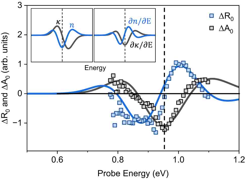
Probe energy-dependent amplitude of the interlayer vibration-induced reflectivity and absorption change,
As depicted in Figure 4, the phonon-induced transition energy shift and narrowing contribute to the modulation of energy-dependent refractive index (n) and extinction coefficient (κ), illustrated in the inset of Figure 5. Assuming that the optical transition is close to the Brillouin zone center (Γ point), we find that the dispersion of the deformation potential (∂E/∂Q) is negligible in comparison to the dispersion of changes in n and κ changes by ΔQ [31]. This assumption leads to a dependence of ∂n/∂E and ∂κ/∂E on the observed amplitude of the TR/TA modulation, as demonstrated in Figure 5. The experimental TR/TA amplitude by phonon is well reproduced with schematic ∂n/∂E and ∂κ/∂E. This observation strongly supports that the modulation of TR/TA was predominantly governed by changes in n and κ, respectively, driven by the interlayer vibration-induced transition energy shift and narrowing.
We further validate the observed interlayer vibration-induced changes in NIR resonance through DFT calculations. These calculations involved applying an out-of-plane strain to modify the interlayer distance. The DFT calculation were carried out for both relaxed and strained bulk Bi2Se3, considering spin–orbit coupling and vdW interactions. We used the Quantum Espresso [32], [33] package implemented in Material Square and the generalized gradient approximation with the Perdew–Burke–Ernzerhof functional [34], [35] to approximate the exchange calculations. To include spin–orbit interactions and vdW interactions [36] between the quintuple layers for all calculations, we chose a full-relativistic norm-conserving pseudopotential and applied the DFT-D3 method correction. The cut-off kinetic energy of the wave function was 85 Ry. The Brillouin zone was automatically sampled using 9 × 9 × 1 Monkhorst–Pack meshes. The convergence threshold and force were 10−8 eV and 10−2 eV/Å, respectively. After the convergence test, we performed variable-cell relaxation to obtain a fully relaxed bulk hexagonal unit cell and determine the atomic positions of Bi2Se3. The calculated lattice parameters for the fully relaxed bulk Bi2Se3 were a = b = 4.18 Å and c = 28.88 Å, consistent with previous reports [37], [38]. We also varied the interlayer distance between QLs and the lattice parameter c without changing the atomic position of each atom inside QL to model the atomic structure changes induced by light-induced strain. Subsequently, density of state (DOS) calculations were performed nonself-consistently with denser meshes of 27 × 27 × 3 using the tetrahedron method.
To compare with DFT calculations, we simulate the photo-induced strain amplitude by considering the electronic and thermal stresses generated by the deformation potential (D) and thermoelasticity [15]. We ignored the inverse-piezo effects that did not correspond to the Bi2Se3 crystal. Electronic stress was obtained with D and the excited carrier density (n ex ) as −D n ex . We adopted herein a previously determined D of 22 eV [39]. Using an optical constant from Figure 1(b), n ex was estimated as 5.8 × 1019 cm−3. For thermal stress (σ TE = −3βBΔT L ) obtained by increasing the lattice temperature (ΔT L ), we employed the linear expansion coefficient (β) and bulk modulus (B) from the literature [40], [41]. The ΔT L changes were obtained from the simplified relation [42] of F pump/(ξC p ), where F pump is the pump fluence and C p = 2.8 J K−1 cm−3 is the lattice heat capacity at 300 K [43]. The calculated electronic and thermal stresses were 0.11 and 0.03 GPa, respectively. The minus sign in the obtained stress indicated an expansion. The subsequent tensile strain along the longitudinal direction was 0.36 %. For the DFT calculation, we applied 1 % strain to emphasize the band structure changes under tensile strain.
In Figure 6, we display the calculated electronic band structure and the total density of states (DOS) for both relaxed and 1 % strained Bi2Se3. The band structure near the Γ point contracts when subjected to a 1 % tensile strain, resulting in a reduction of the energy gap by approximately 30 meV. Comparing this to the observed energy shift of about 14 meV, the theoretical calculations align well with the experimental results. By plotting the band structure and the DOS together, we found optical transition of approximately 1 eV for the unstrained Bi2Se3, which was consistent with the results of previous studies [16], [18]. This value slightly decreased due to the band shift. The narrowing of the NIR resonance through interlayer vibration was attributed to the band shrinkage near the Γ point under a longitudinal strain. The electronic band shrinkage by the interlayer vibrations was caused by the observed AO effects. In other words, the SOC effect changed when the Coulomb interaction between Se atoms changed [25], [41], [44]. Throughout this process, electronic bands may contract in momentum space while maintaining the total DOS, which attributes to the observed ultrafast modulation of NIR spectra in Bi2Se3 vdW thin films by light-driven interlayer vibrations along longitudinal direction.
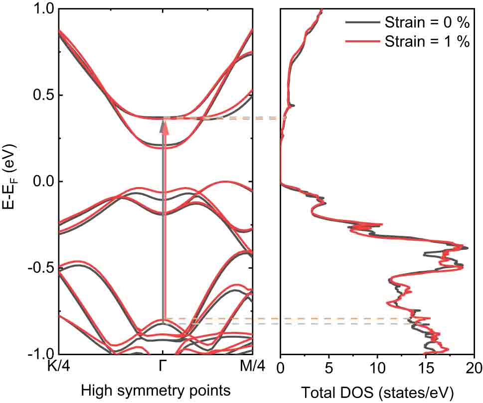
Electronic band structure and total density of states (DOS) of the relaxed (unstrained) and 1 % strained bulk Bi2Se3. The band structure was calculated along the path of the quarter of high-symmetry points K, Γ, and M. The interband transition energy of the relaxed Bi2Se3 was determined as 1.19 eV, which decreased to approximately 30 meV when 1 % of tensile strain was applied. This result supported the pump–probe experimental result well.
3 Conclusions
In this study, we utilized ultrafast NIR spectroscopy and DFT calculations to showcase acousto-optic effects at the broad NIR range in Bi2Se3 vdW thin films. Ultrafast lasers were employed to induce interlayer vibrations in the range of hundreds of GHz. Thickness control provided frequency tunability from sub-GHz to sub-THz within the crystal. These ultrafast acoustic interactions persisted for 100 ps, a duration sufficiently long compared to the lattice vibration period. The vibrational modes demonstrated high speed, rendering them suitable for narrow bandwidth applications. Importantly, the incoherent electronic background was relaxed under ultrafast (∼2 ps) and ultraslow (∼ns) conditions, offering an almost flat incoherent offset during the acoustic modulation. The excitation of the coherent acoustic phonons was generally based on the excited charge interactions; hence, a flat electronic background was difficult to achieve in the all-optical modulation scheme [12], [13], [45], [46], [47], [48], [49].
Our results demonstrate the interaction of the photoexcited carriers with the lattice, launching unique interlayer vibrations coupled with resonant optical transitions near 1.0 eV. In the microscopic view, the changes in the interlayer distance altered the gap between the electronic bands, showing a corresponding NIR resonance. This led to the resonance energy shift. The NIR resonance indicated asymmetric shift that manifested the line shape modulations. This scheme enables for all-optical modulators by generation and detection of coherent interlayer vibrations, highlighting the potential for future modulators with high frequency and integrability at the nanophotonic scale. Particularly in the NIR spectral range, where Bi2Se3 demonstrates high photo-responsivity [50], [51], this approach holds promise for superior performance in signal detection and processing. However, the modulation depth in reflectivity/absorption induced by interlayer vibrations is on the order of 10−4 in the NIR spectrum, which is small compared to the commercial AO devices. Hence, achieving a large amplitude for such application is essential, reaching a level that is compatible with other conventional measurement systems. The acousto-optic effects can be enhanced by applying bias to promote phonon generation through drifting electrons [52], [53], [54], optomechanical cavities [55], and emerging integrated platforms [56], as the observed interactions between interlayer vibrations and photons occur within a few tens of nanometers.
Funding source: National Research Council of Science and Technology
Award Identifier / Grant number: CAP18054-000
Funding source: DGIST R&D Program of the Ministry of Science and ICT
Award Identifier / Grant number: 24-ET-02
Award Identifier / Grant number: Start-up Fund
Funding source: Korea Institute of Energy Technology Evaluation and Planning
Award Identifier / Grant number: 20224B1010040
Funding source: National Research Foundation of Korea
Award Identifier / Grant number: 2021R1A2C2004324
Award Identifier / Grant number: 2021R1F1A1050726
Award Identifier / Grant number: RS-2023-00208484
Acknowledgments
The authors thank Eui-Choel Shin, Seungil Baek, and Yong-Hyun Kim for fruitful discussions.
-
Research funding: This work was supported by the National Research Foundation of Korea (NRF) funded by the Ministry of Science, ICT & Future Planning, Korea (RS-2023-00208484, 2021R1F1A1050726, 2021R1A2C2004324) and the National Research Council of Science & Technology (NST) grant from the Korean Government (CAP18054-000), and Korea Institute of Energy Technology Evaluation and Planning (KETEP) funded by the Korea government (MOTIE) (20224B1010040). This work was also supported by the DGIST R&D Program of the Ministry of Science and ICT (24-ET-02) Start-up Fund.
-
Author contributions: All authors have accepted responsibility for the entire content of this manuscript and approved its submission.
-
Conflict of interest: Authors state no conflicts of interest.
-
Informed consent: Informed consent was obtained from all individuals included in this study.
-
Ethical approval: The conducted research is not related to either human or animals use.
-
Data availability: Data sharing is not applicable to this article as no datasets were generated or analyzed during the current study.
References
[1] N. Savage, “Acousto-optic devices,” Nat. Photon., vol. 4, no. 10, pp. 728–739, 2010. https://doi.org/10.1038/nphoton.2010.229.Search in Google Scholar
[2] F. Kurtz, C. Ropers, and G. Herink, “Resonant excitation and all-optical switching of femtosecond soliton molecules,” Nat. Photon., vol. 14, no. 1, pp. 9–13, 2020. https://doi.org/10.1038/s41566-019-0530-3.Search in Google Scholar
[3] F. Kurtz, C. Ropers, and G. Herink, “Shaping the future of manipulation,” Nat. Photon., vol. 5, no. 6, pp. 335–342, 2011. https://doi.org/10.1038/nphoton.2011.80.Search in Google Scholar
[4] B. Li, Q. Lin, and M. Li, “Frequency–angular resolving LiDAR using chip-scale acousto-optic beam steering,” Nature, vol. 620, no. 7973, pp. 316–322, 2011. https://doi.org/10.1038/s41586-023-06201-6.Search in Google Scholar PubMed
[5] J. H. Kim, M. C. Kuzyk, K. Han, H. Wang, and G. Bahl, “Non-reciprocal Brillouin scattering induced transparency,” Nat. Phys., vol. 11, no. 3, pp. 275–280, 2015. https://doi.org/10.1038/nphys3236.Search in Google Scholar
[6] E. A. Kittlaus, N. T. Otterstrom, P. Kharel, S. Gertler, and P. T. Rakich, “Nonreciprocal interband Brillouin modulation,” Nat. Photon., vol. 12, no. 10, pp. 613–619, 2018. https://doi.org/10.1038/s41566-018-0254-9.Search in Google Scholar
[7] H. Kim and H. Shin, “Active information manipulation via optically driven acoustic-wave interference,” Nano Lett., vol. 21, no. 17, pp. 7270–7276, 2021. https://doi.org/10.1021/acs.nanolett.1c02314.Search in Google Scholar PubMed
[8] J. Lu, et al.., “Recent progress of dynamic mode manipulation via acousto-optic interactions in few-mode fiber lasers: mechanism, device and applications,” Nanophotonics, vol. 10, no. 3, pp. 983–1010, 2020. https://doi.org/10.1515/nanoph-2020-0461.Search in Google Scholar
[9] C. J. Sarabalis, et al.., “Acousto-optic modulation of a wavelength-scale waveguide,” Optica, vol. 8, no. 4, pp. 477–483, 2021. https://doi.org/10.1364/optica.413401.Search in Google Scholar
[10] J. Beller and L. Shao, “Acousto-optic modulators integrated on-chip,” Light Sci. Appl., vol. 11, no. 1, p. 240, 2022. https://doi.org/10.1038/s41377-022-00928-z.Search in Google Scholar PubMed PubMed Central
[11] Z. Peng, X. Chen, Y. Fan, D. J. Srolovitz, and D. Lei, “Strain engineering of 2D semiconductors and graphene: from strain fields to band-structure tuning and photonic applications,” Light Sci. Appl., vol. 9, no. 1, p. 190, 2020. https://doi.org/10.1038/s41377-020-00421-5.Search in Google Scholar PubMed PubMed Central
[12] M. Lejman, et al.., “Ultrafast acousto-optic mode conversion in optically birefringent ferroelectrics,” Nat. Commun., vol. 7, no. 1, pp. 1–10, 2016. https://doi.org/10.1038/ncomms12345.Search in Google Scholar PubMed PubMed Central
[13] E. Baldini, et al.., “Exciton control in a room temperature bulk semiconductor with coherent strain pulses,” Sci. Adv., vol. 5, no. 11, p. eaax2937, 2019. https://doi.org/10.1126/sciadv.aax2937.Search in Google Scholar PubMed PubMed Central
[14] E. Baldini, T. Palmieri, A. Dominguez, P. Ruello, A. Rubio, and M. Chergui, “Phonon-driven selective modulation of exciton oscillator strengths in anatase TiO2 nanoparticles,” Nano Lett., vol. 18, no. 8, pp. 5007–5014, 2018. https://doi.org/10.1021/acs.nanolett.8b01837.Search in Google Scholar PubMed
[15] P. Ruello and V. E. Gusev, “Physical mechanisms of coherent acoustic phonons generation by ultrafast laser action,” Ultrasonics, vol. 56, pp. 21–35, 2015. https://doi.org/10.1016/j.ultras.2014.06.004.Search in Google Scholar PubMed
[16] M. Fang, et al.., “Layer-dependent dielectric permittivity of topological insulator Bi2Se3 thin films,” Appl. Surf. Sci., vol. 509, p. 144822, 2020. https://doi.org/10.1016/j.apsusc.2019.144822.Search in Google Scholar
[17] M. R. Filip, C. E. Patrick, and F. Giustino, “GW quasiparticle band structures of stibnite, antimonselite, bismuthinite, and guanajuatite,” Phys. Rev. B, vol. 87, no. 20, p. 205125, 2013. https://doi.org/10.1103/physrevb.87.205125.Search in Google Scholar
[18] M. Eddrief, F. Vidal, and B. Gallas, “Optical properties of Bi2Se3: from bulk to ultrathin films,” J. Phys. D: Appl. Phys., vol. 49, no. 50, p. 505304, 2016. https://doi.org/10.1088/0022-3727/49/50/505304.Search in Google Scholar
[19] Y. D. Glinka, S. Babakiray, T. A. Johnson, M. B. Holcomb, and A. D. Lederman, “Ultrafast carrier dynamics in thin-films of the topological insulator Bi2Se3,” Appl. Phys. Lett., vol. 103, no. 15, p. 151903, 2013. https://doi.org/10.1063/1.4824821.Search in Google Scholar
[20] M. Weis, et al.., “Quantum size effect on charges and phonons ultrafast dynamics in atomically controlled nanolayers of topological insulators Bi2Te3,” Sci. Rep., vol. 7, no. 1, p. 13782, 2017. https://doi.org/10.1038/s41598-017-12920-4.Search in Google Scholar PubMed PubMed Central
[21] P. H. Tan, et al.., “The shear mode of multilayer graphene,” Nat. Mater., vol. 11, no. 4, pp. 294–300, 2012. https://doi.org/10.1038/nmat3245.Search in Google Scholar PubMed
[22] D. Boschetto, et al.., “Real-time observation of interlayer vibrations in bilayer and few-layer graphene,” Nano Lett., vol. 13, no. 10, pp. 4620–4623, 2013. https://doi.org/10.1021/nl401713h.Search in Google Scholar PubMed
[23] R. He, et al.., “Interlayer breathing and shear modes in NbSe2 atomic layers,” 2D Mater., vol. 3, no. 3, p. 031008, 2016. https://doi.org/10.1088/2053-1583/3/3/031008.Search in Google Scholar
[24] L. Liang, J. Zhang, B. G. Sumpter, Q. H. Tan, P. H. Tan, and V. Meunier, “Low-frequency shear and layer-breathing modes in Raman scattering of two-dimensional materials,” ACS Nano, vol. 11, no. 12, pp. 11777–11802, 2017. https://doi.org/10.1021/acsnano.7b06551.Search in Google Scholar PubMed
[25] S. Kim, et al.., “Ultrafast carrier–lattice interactions and interlayer modulations of Bi2Se3 by X-ray free-electron laser diffraction,” Nano Lett., vol. 21, no. 20, pp. 8554–8562, 2021. https://doi.org/10.1021/acs.nanolett.1c01424.Search in Google Scholar PubMed
[26] Y. Zhao, et al.., “Interlayer vibrational modes in few-quintuple-layer Bi2Te3 and Bi2Se3 two-dimensional crystals: Raman spectroscopy and first-principles studies,” Phys. Rev. B, vol. 90, no. 24, p. 245428, 2014. https://doi.org/10.1103/physrevb.90.245428.Search in Google Scholar
[27] N. S. Luo, P. Ruggerone, and J. P. Toennies, “Theory of surface vibrations in epitaxial thin films,” Phys. Rev. B, vol. 54, no. 7, p. 5051, 1996. https://doi.org/10.1103/physrevb.54.5051.Search in Google Scholar PubMed
[28] S. Giraud, A. Kundu, and R. Egger, “Electron-phonon scattering in topological insulator thin films,” Phys. Rev. B, vol. 85, no. 3, p. 035441, 2012. https://doi.org/10.1103/physrevb.85.035441.Search in Google Scholar
[29] Y. D. Glinka, S. Babakiray, T. A. Johnson, and D. Lederman, “Acoustic phonon dynamics in thin-films of the topological insulator Bi2Se3,” J. Appl. Phys., vol. 117, no. 16, p. 165703, 2015. https://doi.org/10.1063/1.4919274.Search in Google Scholar
[30] G. Prakash, K. Pal, U. V. Waghmare, and A. K. Sood, “Anomalous temperature dependence of optical and acoustic phonons in Bi2Se3 arising from stacking faults,” Phys. Scr., vol. 94, no. 11, p. 115706, 2019. https://doi.org/10.1088/1402-4896/ab30f5.Search in Google Scholar
[31] A. Bartels, T. Dekorsy, H. Kurz, and K. Köhler, “Coherent zone-folded longitudinal acoustic phonons in semiconductor superlattices: excitation and detection,” Phys. Rev. Lett., vol. 82, no. 5, p. 1044, 1999. https://doi.org/10.1103/physrevlett.82.1044.Search in Google Scholar
[32] P. Giannozzi, et al.., “QUANTUM ESPRESSO: a modular and open-source software project for quantum simulations of materials,” J. Phys. Condens., vol. 21, no. 39, p. 395502, 2009. https://doi.org/10.1088/0953-8984/21/39/395502.Search in Google Scholar PubMed
[33] P. Giannozzi, et al.., “Advanced capabilities for materials modelling with Quantum ESPRESSO,” J. Phys. Condens., vol. 29, no. 46, p. 465901, 2017. https://doi.org/10.1088/1361-648x/aa8f79.Search in Google Scholar PubMed
[34] G. Kresse and D. Joubert, “From ultrasoft pseudopotentials to the projector augmented-wave method,” Phys. Rev. B, vol. 59, no. 3, p. 1758, 1999. https://doi.org/10.1103/physrevb.59.1758.Search in Google Scholar
[35] J. P. Perdew, K. Burke, and M. Ernzerhof, “Generalized gradient approximation made simple,” Phys. Rev. Lett., vol. 77, no. 18, p. 3865, 1996. https://doi.org/10.1103/physrevlett.77.3865.Search in Google Scholar
[36] S. Grimme, S. Ehrlich, and L. Goerigk, “Effect of the damping function in dispersion corrected density functional theory,” J. Comput. Chem., vol. 32, no. 7, pp. 1456–1465, 2011. https://doi.org/10.1002/jcc.21759.Search in Google Scholar PubMed
[37] H. Aramberri and M. C. Muñoz, “Strain effects in topological insulators: topological order and the emergence of switchable topological interface states in Sb2Te3/Bi2Te3 heterojunctions,” Phys. Rev. B, vol. 95, no. 20, p. 205422, 2017. https://doi.org/10.1103/physrevb.95.205422.Search in Google Scholar
[38] H. Aramberri and M. C. Muñoz, “Strain-driven tunable topological states in Bi2Se3,” J. Phys Mater., vol. 1, no. 1, p. 015009, 2018. https://doi.org/10.1088/2515-7639/aadf74.Search in Google Scholar
[39] D. Kim, et al.., “Intrinsic electron-phonon resistivity of Bi2Se3 in the topological regime,” Phys. Rev. Lett., vol. 109, no. 16, p. 166801, 2012. https://doi.org/10.1103/physrevlett.109.166801.Search in Google Scholar PubMed
[40] X. Chen, et al.., “Thermal expansion coefficients of Bi2Se3 and Sb2Te3 crystals from 10 K to 270 K,” Appl. Phys. Lett., vol. 99, no. 26, p. 261912, 2011. https://doi.org/10.1063/1.3672198.Search in Google Scholar
[41] S. M. Young, S. Chowdhury, E. J. Walter, E. J. Mele, C. L. Kane, and A. M. Rappe, “Theoretical investigation of the evolution of the topological phase of Bi2Se3 under mechanical strain,” Phys. Rev. B, vol. 84, no. 8, p. 085106, 2011. https://doi.org/10.1103/physrevb.84.085106.Search in Google Scholar
[42] T. Saito, O. Matsuda, and O. B. Wright, “Picosecond acoustic phonon pulse generation in nickel and chromium,” Phys. Rev. B, vol. 67, no. 20, p. 205421, 2003. https://doi.org/10.1103/physrevb.67.205421.Search in Google Scholar
[43] R. Sultana, et al.., “Electrical, thermal and spectroscopic characterization of Bulk Bi2Se3 topological insulator,” J. Supercond. Nov. Magn., vol. 30, no. 8, pp. 2031–2036, 2017. https://doi.org/10.1007/s10948-017-4173-7.Search in Google Scholar
[44] Y. Liu, et al.., “Tuning Dirac states by strain in the topological insulator Bi2Se3,” Nat. Phys., vol. 10, no. 4, pp. 294–299, 2014. https://doi.org/10.1038/nphys2898.Search in Google Scholar
[45] T. Mishina, K. Nitta, and Y. Masumoto, “Coherent lattice vibration of interlayer shearing mode of graphite,” Phys. Rev. B, vol. 62, no. 4, p. 2908, 2000. https://doi.org/10.1103/physrevb.62.2908.Search in Google Scholar
[46] F. M. Bartram, et al.., “Ultrafast coherent interlayer phonon dynamics in atomically thin layers of MnBi2Te4,” npj Quantum Mater., vol. 7, no. 1, p. 84, 2022. https://doi.org/10.1038/s41535-022-00495-x.Search in Google Scholar
[47] H. D. Boggiano, R. Berté, A. F. Scarpettini, E. Cortés, S. A. Maier, and A. V. Bragas, “Determination of nanoscale mechanical properties of polymers via plasmonic nanoantennas,” ACS Photon., vol. 7, no. 6, pp. 1403–1409, 2020. https://doi.org/10.1021/acsphotonics.0c00631.Search in Google Scholar
[48] J. Wang, J. Zhu, Y. Jiang, M. Li, K. Yu, and G. P. Wang, “Observation of elastic heterogeneity and phase evolution in 2D layered perovskites using coherent acoustic phonons,” Nanophotonics, vol. 10, no. 16, pp. 4009–4017, 2021. https://doi.org/10.1515/nanoph-2021-0358.Search in Google Scholar
[49] S. Bae, et al.., “K-point longitudinal acoustic phonons are responsible for ultrafast intervalley scattering in monolayer MoSe2,” Nat. Commun., vol. 13, no. 1, p. 4279, 2022. https://doi.org/10.1038/s41467-022-32008-6.Search in Google Scholar PubMed PubMed Central
[50] F. Wang, et al.., “Submillimeter 2D Bi2Se3 flakes toward high-performance infrared photodetection at optical communication wavelength,” Adv. Funct. Mater., vol. 28, no. 33, p. 1802707, 2018. https://doi.org/10.1002/adfm.201802707.Search in Google Scholar
[51] M. Yang, et al.., “Ultrahigh stability 3D TI Bi2Se3/MoO3 thin film heterojunction infrared photodetector at optical communication waveband,” Adv. Funct. Mater., vol. 30, no. 12, p. 1909659, 2020. https://doi.org/10.1002/adfm.201909659.Search in Google Scholar
[52] S. M. Komirenko, K. W. Kim, A. A. Demidenko, V. A. Kochelap, and M. A. Stroscio, “Generation and amplification of sub-THz coherent acoustic phonons under the drift of two-dimensional electrons,” Phys. Rev. B, vol. 62, no. 11, p. 7459, 2000. https://doi.org/10.1103/physrevb.62.7459.Search in Google Scholar
[53] K. Shinokita, K. Reimann, M. Woerner, T. Elsaesser, R. Hey, and C. Flytzanis, “Strong amplification of coherent acoustic phonons by intraminiband currents in a semiconductor superlattice,” Phys. Rev. Lett., vol. 116, no. 7, p. 075504, 2016. https://doi.org/10.1103/physrevlett.116.075504.Search in Google Scholar PubMed
[54] R. P. Beardsley, A. V. Akimov, M. Henini, and A. J. Kent, “Coherent terahertz sound amplification and spectral line narrowing in a Stark ladder superlattice,” Phys. Rev. Lett., vol. 104, no. 8, p. 085501, 2010. https://doi.org/10.1103/physrevlett.104.085501.Search in Google Scholar PubMed
[55] G. S. Maccabe, et al.., “Nano-acoustic resonator with ultralong phonon lifetime,” Science, vol. 370, no. 6518, pp. 840–843, 2020. https://doi.org/10.1126/science.abc7312.Search in Google Scholar PubMed
[56] S. R. Kachiraju, et al.., “Coupled surface plasmon–phonon polariton nanocavity arrays for enhanced mid-infrared absorption,” Nanophotonics, vol. 11, no. 20, pp. 4489–4498, 2022. https://doi.org/10.1515/nanoph-2022-0339.Search in Google Scholar
© 2024 the author(s), published by De Gruyter, Berlin/Boston
This work is licensed under the Creative Commons Attribution 4.0 International License.
Articles in the same Issue
- Frontmatter
- Editorial
- Enabling new frontiers of nanophotonics with metamaterials, photonic crystals, and plasmonics
- Reviews
- Rational design of arbitrary topology in three-dimensional space via inverse calculation of phase modulation
- Frequency comb measurements for 6G terahertz nano/microphotonics and metamaterials
- Research Articles
- Electromagnetic signal propagation through lossy media via surface electromagnetic waves
- Mode-cleaning in antisymmetrically modulated non-Hermitian waveguides
- Hollow core optical fiber enabled by epsilon-near-zero material
- Photoluminescence lifetime engineering via organic resonant films with molecular aggregates
- Photoluminescence emission and Raman enhancement in TERS: an experimental and analytic revisiting
- Scalable hot carrier–assisted silicon photodetector array based on ultrathin gold film
- Ultrafast acousto-optic modulation at the near-infrared spectral range by interlayer vibrations
- Probing the multi-disordered nanoscale alloy at the interface of lateral heterostructure of MoS2–WS2
- Topological phase transition and surface states in a non-Abelian charged nodal line photonic crystal
- Ultraviolet light scattering by a silicon Bethe hole
- Exploring plasmonic gradient metasurfaces for enhanced optical sensing in the visible spectrum
- Thermally tunable binary-phase VO2 metasurfaces for switchable holography and digital encryption
- Electrochromic nanopixels with optical duality for optical encryption applications
- Broadband giant nonlinear response using electrically tunable polaritonic metasurfaces
- Mechanically processed, vacuum- and etch-free fabrication of metal-wire-embedded microtrenches interconnected by semiconductor nanowires for flexible bending-sensitive optoelectronic sensors
- Formation of hollow silver nanoparticles under irradiation with ultrashort laser pulses
- Dry synthesis of bi-layer nanoporous metal films as plasmonic metamaterial
- Three-dimensional surface lattice plasmon resonance effect from plasmonic inclined nanostructures via one-step stencil lithography
- Generic characterization method for nano-gratings using deep-neural-network-assisted ellipsometry
- Photonic advantage of optical encoders