All optical tunable RF filter using elemental antimony
-
Samarth Aggarwal
 ,
Nikolaos Farmakidis
,
Nikolaos Farmakidis


Abstract
In the past decade, the proliferation of modern telecommunication technologies, including 5G, and the widespread adoption of the Internet-of-things (IoT) have led to an unprecedented surge in data generation and transmission. This surge has created an escalating demand for advanced signal processing capabilities. Microwave photonic (MWP) processors offer a promising solution to satisfy this unprecedented demand for data processing by capitalising on the high bandwidth and low latency achievable by optical systems. In this work, we introduce an integrated MWP processing unit for all-optical RF filtering using elemental antimony. We exploit the crystallisation dynamics of antimony to demonstrate a photonic leaky integrator, which is configured to operate as a first-order low-pass filter with a bandwidth of 300 kHz and ultra-compact footprint of 16 × 16 μm2. We experimentally demonstrate the implementation of such a filter as an envelope detector to demodulate an amplitude-modulated signal. Finally, a discussion on achieving bandwidth tunability is presented.
1 Introduction
Microwave photonic (MWP) processors offer inherent benefits offered by photonics such as insensitivity to electromagnetic interference [1]. So far, there has been significant interest in using MWP processors for filtering operations in the optical domain [2]–[7]. Such MWP processors can be embedded with optical sensors in IoT-based devices to pre-process real-time data. This would reduce the computational load while avoiding the losses associated with electro-optic conversions in the processing unit. Various MWP processors have been demonstrated as all-optical delay lines [8], [9] and for filtering operations such as notch filters [10]. Most implementations of MWP processors so far have utilized coherent light sources and often use resonator-coupled Mach–Zehnder interferometer (MZI) devices [11]–[14], photonic crystals [9] or are based on nonlinear effects such as stimulated Brillouin scattering (SBS) [15]–[19]. MWP filters using ring resonators and interferometers suffer from large device footprints and have a periodic transfer function limited by their free spectral range [19], ultimately limiting the tuning bandwidth. For SBS-based MPWs, while low-power integrated solutions have been proposed [16], using chalcogenide waveguides makes them incompatible with the CMOS process, thus limiting scalability and adoption.
While current integrated solutions can achieve satisfactory tunability and high bandwidth [20], [21], they are still limited by their large footprints and incompatibility with foundry processes. To achieve adoption of such MWP processors, there have been efforts to reduce their overall device footprint and energy budget, mainly using integrated photonic solutions [22], [23]. The increasing maturity of integrated photonic platforms has allowed for co-integration of key components such as lasers and modulators [4], [24], [3].
This work introduces an ultra-compact MWP filter based on elemental antimony. This material was recently demonstrated by the authors (not all authors were involved in the previous work) to function as a dynamic phase change material (PCM) [25], [26]. These properties were explored for photonic phase change memory and optical weighting [25], [26]. Such antimony-based memory has been shown to have a tuneable, volatile behaviour in milliseconds to seconds, depending on the device geometry. This volatility has been attributed to the spontaneous recrystallisation of the amorphous phase. In previous work, a thickness-dependent volatile behaviour for thin film antimony has been demonstrated [25]–[28]. Here, we exploit the material-level properties, specifically the spontaneous recrystallisation of antimony as a leaky integrator and demonstrate a first-order low pass filter with a bandwidth of 300 kHz (3 dB).
In Table 1 we summarise various MWP filters techniques reported in literature. It is worth noting that our current proof of concept work is limited to a narrow band low pass filter. Nevertheless the bandwidth of such a system can further be increased by designing better photonic circuits, integrating functional materials and resonator based MWP designs. The purpose of this work is to introduce MWP based on elemental antimony. Our implementation can also be readily adapted for use with phase change materials demonstrating multilevel memory operation and tuneable volatility such as Ge2Se2Te5 [29], Ge3Sb2Te6 [30] and VO2 [31], amongst others.
Summary of various MWP filters technologies.
| Technique | Filter type | Bandwidth (3 dB) | Footprint | Platform | Reference |
|---|---|---|---|---|---|
| Photonic crystal- delay line | Notch, bandpass | 50 GHz | 1.5 mm long | GaInP/GaAs | [9] |
| MZI-ring resonator | Notch | 635 MHz | 1.75 mm2 | Si | [7] |
| Ring-MZI | Notch, bandpass | 1–2 GHz | 6 × 4 mm2 | InP | [3] |
| Ring resonator | Notch | 247–840 MHz, | 8.73 mm long | SiN | [12] |
| SBS | Stop-pass | 32–88 MHz | 6.5-cm-long | As2S3 | [16] |
| SBS | Notch filter | 126 MHz | 6.5-cm long | As2S3 | [18] |
| PCM | Low-pass filter | 300 kHz | 16 × 16 μm2 | Si | This work |
-
MZI, Mach Zender interferometer; SBS, stimulated Brillouin scattering; PCM, phase change material.
2 Results
2.1 Filter design
The concept of a microwave photonic filter is demonstrated in Figure 1(a). The design consists of a photonic waveguide crossing with a thin film of antimony (Sb) on the waveguide at the crossing. As demonstrated in previous work [25], [26], femtosecond (fs) pulses can result in amorphisation of Sb. Crystalline and amorphous antimony have different optical absorption coefficient (k = 2.81 for crystalline and k = 0.61 for amorphous phase at 1550 nm) [26], thus resulting in a change in the transmission state of the photonic device, from low transmission to higher transmission. Different transmission states are achieved depending on the amplitude of the amorphisation pulses.

Antimony based microwave photonic filter. (a) Schematic of Sb-PCM based photonic filter design. An arbitrary rf signal is discretised and amplitude modulated on a fs pulse series. These modulated fs pulses (modulator-out) are then used to amorphize Sb. A CW laser is used to observe the change in transmission (filter-out). (b) False coloured optical image of the fabricated photonic device consisting of a waveguide crossing with 5 nm Sb sputtered on top and grating couplers to couple light to perform filter operation.
In our implementation of a photonic RF filter, an arbitrary RF input signal is discretised, and amplitude modulated on a fs pulse series (Fs-pulse train) using an optical modulator as shown in Figure 1(a). Here the pulse repletion rate determines the sampling rate of the RF input signal. The modulated fs pulses (modulator-out) are then used to switch antimony. A continuous wave (CW) laser is used in the probe line, and a photodetector records the transmission change (filter-output). In our experiments, a fs pulse with a repetition rate of 3.3 MHz and pulse width of 800 fs is used.
In Figure 1(b), we show a false-coloured optical microscope image of the photonic device used for implementing an integrated photonic RF filter. The device consists of a 16 × 16 μm2 waveguide crossing, with grating couplers to couple light in and out of the device. The device consists of a 2 × 2 μm2 of 5 nm-thick ‘active’ material, i.e., Sb thin film. The device is based on a standard 220 nm silicon on insulator (SOI) photonic platform. A half-etched, single-mode ridge waveguide for operation at 1550 nm wavelength is fabricated via electron beam lithography.
2.2 Leaky integrator
First, we investigate the switching response of our device using fs pulses by recording the change in transmission using a low-power CW probe laser. The response to single fs pulses of increasing pulse energy from P1 to P8 (185 pJ–486 pJ), is recorded in Figure 2(a). Starting with the low transmission crystalline phase, high energy single fs pulse leads to amorphisation, thus increasing the transmission. As determined in earlier work [25], the amorphisation time using femtosecond pulse is 2 ns. Due to the spontaneous recrystallisation of the amorphous phase, a volatile change in transmission is observed. This volatile switching response of Sb has a response equivalent to the impulse response of a leaky integrator.

Switching response of antimony device. (a) Volatile switching of antimony with varying pulse energies from P1–P8 (185 pJ, 246 pJ, 312 pJ, 324 pJ, 338 pJ, 374 pJ, 426 pJ, 486 pJ, respectively). (b) Impulse response of a leaky integrator is fitted with the switching response for the Sb filter device. (c–d) Superposition of impulse response for Sb device. Experimentally obtained response (in black) is fitted to simulated responses (in blue and red). The summation of two simulated responses (in green) matches well with the experimentally obtained response for ‘long’ separation of 30 ms and a ‘short’ duration of 5 ms, respectively.
For a stream of sampled data, a leaky integrator adds up the input data while ‘forgetting’ some of the previous data, i.e. ‘leaking’ it. A leaky integrator can thus be used to average a data stream, effectively functioning like a low-pass filter and is represented by the following equation:
where x[n] is the nth data sample, and alpha (α) is the leaky parameter. Thus, for α = 1, no averaging takes place and reducing α results in stronger averaging. This can be further analysed by taking the z-transform to get the following:
This can then be rearranged to get the transfer function H(z):
Thus, the impulse response of a leaky integrator can be written as
Next, we explore the superposition properties of the device. For a linear filter with response H(s) and stimulus s
1 and s
2,
In the second case, the two pulses are separated by a ‘short’ duration of 5 ms. As before, the impulse responses of 2 pulses separated by 5 ms are plotted as dotted lines in blue and red in Figure 2(d). The summation of the two impulse responses is shown in green. The impulse response of a leaky integrator fits well with the transmission response of the Sb filter device, thus showing the linearity of stimulus responses.
It is worth noting that the switching and the recrystallisation dynamics of a PCM-based device is a complex function of the pulse amplitude, number of pulses and the transmission state of the device. While working with many pulses, the recrystallisation dynamics of the material can be enhanced due formation of a large number of subcritical nuclei [32] during melt-quench. Moreover, switching pulses are absorbed weakly while in a higher transmission state, resulting in saturation of the achievable transmission level. We use this richness present in our device to demonstrate a low-pass filter, and the exact nature of this phenomenon will require further studies.
2.3 Frequency response
Any input signal can be discretised in time and represented as impulses with weighted amplitude and shifted in time. Thus, the response of such input signals through the Sb filter device can be predicted easily as the sum of the impulse response of Sb filter cells weighted with the impulse amplitude. Another consequence of this property is that the output at any time ‘t’ is the weighted average of all the previous impulse responses. This results in the smoothing of the input signal, or in other words, performs a low-pass filter operation on the input data.
Next, we test this property of a low-pass filter for our device. As described previously, while keeping the pulse repetition rate fixed at 3.3 MHz, rectified sine waves of varying frequency are modulated onto a train of femtosecond pulses. The transmission response of the Sb device for various input signals is reported in Figure S3. It is observed that increasing the input signal frequency decreases the amplitude of the output sine wave signal, thus acting as a low-pass filter. When Sb is switched to amorphous phase the transmission of our device increases initially, but subsequently drops due to spontaneous recrystallisation. This results in jitter in the device response. This jitter noise can further be reduced by increasing the sampling rate.
Next, the analysis for individual frequency response is performed by taking the fast Fourier transformation (FFT) of the output response. The amplitude (in dB) of the device output is plotted for various frequencies in Figure 3. This plot determines the pass band and the stop band for the Sb device filter. A bandwidth of 300 kHz (at 3 dB loss) with an attenuation of −2 dB/decade is obtained for an integrated photonic RF filter.
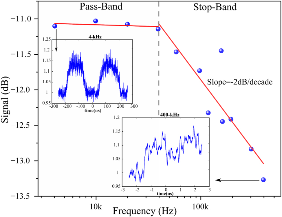
Frequency response analysis of sinusoidal data (details in Figure S3) is performed to determine the pass-band and stop band of the filter. Inset shows the experimentally obtained sine wave response of the device for a low frequency (4 kHz) and high frequency (400 kHz) input signal.
2.4 Envelope detector
An envelope detector takes in a high-frequency amplitude-modulated (AM) signal as input and returns the envelope of this signal, which is the low-pass output. Therefore, to demonstrate the performance of the Sb device as an envelope detector, a 4 kHz sine wave signal is AM with different carrier frequencies ranging from 40 kHz to 2 MHz.
As determined above, the Sb device has a 3 dB bandwidth of 300 kHz. Thus, frequencies above this range are filtered from the input signal. The response of the Sb device for various carrier frequencies is shown in Figure 4(a). As expected, frequencies >300 kHz are filtered from the 4 kHz sine wave signal, observed as a decrease in the carrier signal amplitude, thus showing excellent performance as an envelope detector. To further analyse the performance of the envelope detector, as before, the amplitude of the carrier signal wave is plotted for various frequencies in Figure 4(b). An exponential suppression of the high-frequency signal is observed, thus demonstrating the excellent performance of the Sb device as an envelope detector.
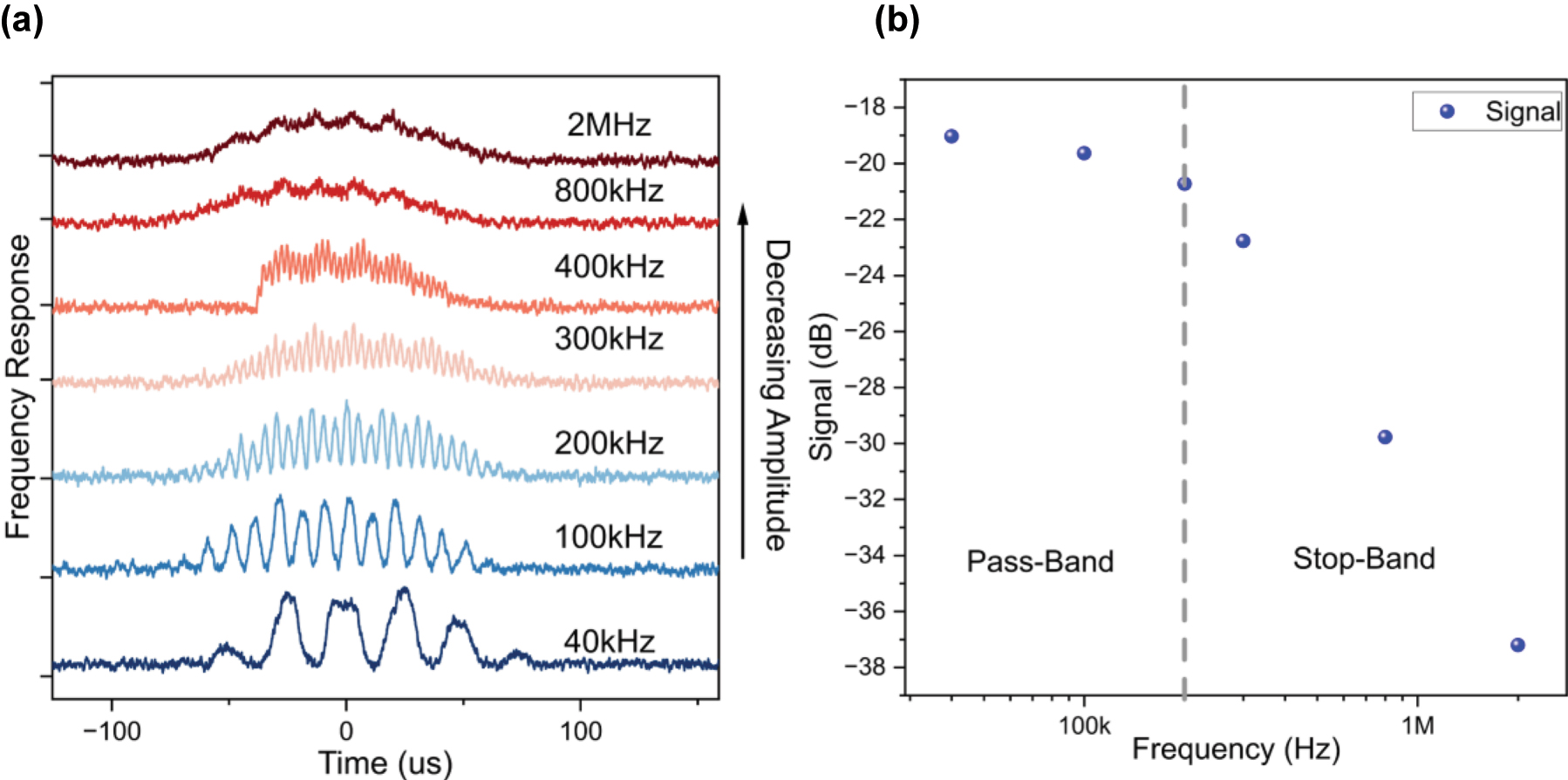
Demonstration of low pass filtering operation.(a) A 4 kHz signal is amplitude modulated with various carrier frequencies, as reported in the graph. Increasing the carrier frequency results in the suppression of the amplitude of the carrier signal. (b) Frequency response analysis of the sine wave of data shown in (a) is performed to determine the pass-band and stop-band of the filter.
3 Tuneable filter
So far, the Sb-based photonic device has been shown to function as a low-pass filter of fixed bandwidth. The frequency response depends on the leaky parameter of the filter. A ‘leaky’ filter would result in a higher cutoff frequency. For the Sb device, the degree of leakiness depends on the retention time of Sb. As demonstrated in previous works, the volatility of Sb can be tuned by varying the probing power [25] and the thickness of the thin film [26], [27].
Therefore, to evaluate the effect of tuning the Sb device’s retention time (volatility) on the input sine wave signal, we simulate the response function for various frequencies in Figure 5. Using fast Fourier transformation, the amplitude of the output response is determined. Increasing the retention time results in a decrease in the low-pass cutoff frequency. Thus, by varying the volatility of the device, a tuneable low-pass filter can be achieved. This tunability can be exploited to achieve complex filtering functions and filter banks using an array of waveguides with a varying film thickness of Sb.
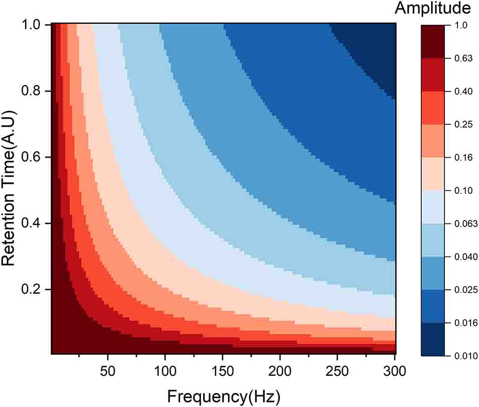
Simulation results demonstrating the effect of retention time of Sb on the frequency cutoff for low-pass filtering.
4 Conclusions
We have demonstrated elemental Sb-based photonics as an integrated MPW processor configured as an optical low-pass filter. We exploit the intrinsic recrystallisation dynamics of the material-system to demonstrate a low-pass filter. The low-pass filter has a 3 dB cutoff bandwidth of 300 kHz and a stop band with an attenuation of −2 dB/decade. We demonstrate an application of this low-pass filter as an envelope detector to demodulate amplitude-modulated signals. We achieve this using an ultracompact device with a footprint of 16 × 16 μm2 with an active area of only 2 × 2 μm2. The small footprint and the ease of fabrication of the device allow for the co-integration of CMOS electronics. While our current demonstration has a fixed bandwidth, we provide discussions for achieving the tuneability of bandwidth by tuning the recrystallisation dynamics by changing the probe power. Such tunability opens up the use of volatile antimony for many applications in signal processing and data encryption.
5 Methods
5.1 Device fabrication
The waveguides are fabricated on a standard 220 nm SOI wafer. The photonic device consisting of the waveguides and the waveguide crossing is patterned using a positive electron beam-sensitive photoresist (AR-P 6200). The waveguides are half etched using reactive ion etching. Using a subsequent lithography process, the windows for Sb deposition are defined. The thin film of antimony is then deposited on the waveguide crossing using an RF sputtering system at a 3.3 nm/min deposition rate in an argon environment using a sputtering target from Testbourne.
5.2 Experimental setup
The experimental setup illustrated in Figure S1 consists of a pump and probe setup as used before, with additional pump modulation electronic circuits described in section S1. A fs laser from Pritel (FFL-TW) is used to switch Sb, and a CW laser (Santec, TSL-550) is used to monitor the transmission change. To achieve the modulation of RF signal-input onto the fs laser pulses, an acoustic optical modulator (AOM) from G&H (Fiber-Q 1550 nm) is used. This results in the discretisation of the RF signal with each sample represented as
Funding source: EPSRC
Award Identifier / Grant number: EP/W022931/1
Award Identifier / Grant number: EP/T023899/1
Award Identifier / Grant number: EP/R001677/1
Funding source: HORIZON EUROPE European Innovation Council
Award Identifier / Grant number: 101046878
Award Identifier / Grant number: 101098717
Funding source: European Union’s Horizon 2020 Framework Programme
Award Identifier / Grant number: 101017237
Funding source: Clarendon Scholarship
Acknowledgments
The authors acknowledge helpful discussions with A. Ne.
-
Research funding: This work has received funding from the European Union’s Horizon 2020 Framework Programme 101017237 (PHOENICS project). HORIZON EUROPE European Innovation Council grant numbers: 101046878 (HYBRAIN project) and 101098717 (RESPITE project). This research was also supported via the Engineering and Physical Sciences Research Council Grants EP/W022931/1, EP/T023899/1, EP/R001677/1, and a Clarendon Scholarship.
-
Author contributions: S.A. and N.F. conceived the original experiments with help from B.D. and J.S.L. M.W. and Z.X. helped in fabrication and experiments. H.B. helped analyse the results and write the paper; H.B. led the work. S.A. and H.B. wrote the manuscript with substantial input from all authors. All authors have accepted responsibility for the entire content of this manuscript and approved its submission.
-
Conflict of interest: Authors state no conflicts of interest.
-
Data availability: The data that support the findings of this study are available from the corresponding author upon reasonable request.
References
[1] J. Capmany, B. Ortega, and D. Pastor, “A tutorial on microwave photonic filters,” J. Lightwave Technol., vol. 24, no. 1, pp. 201–229, 2006. https://doi.org/10.1109/JLT.2005.860478.Suche in Google Scholar
[2] J. Capmany, I. Gasulla, and D. Pérez, “Microwave photonics: the programmable processor,” Nat. Photonics, vol. 10, no. 1, pp. 6–8, 2016. https://doi.org/10.1038/nphoton.2015.254.Suche in Google Scholar
[3] J. S. Fandiño, P. Muñoz, D. Doménech, and J. Capmany, “A monolithic integrated photonic microwave filter,” Nat. Photonics, vol. 11, no. 2, pp. 124–129, 2016. https://doi.org/10.1038/nphoton.2016.233.Suche in Google Scholar
[4] E. J. Norberg, R. S. Guzzon, J. S. Parker, L. A. Johansson, and L. A. Coldren, “Programmable photonic microwave filters monolithically integrated in InP/InGaAsP,” J. Lightwave Technol., vol. 29, no. 11, pp. 1611–1619, 2011. https://doi.org/10.1109/jlt.2011.2134073.Suche in Google Scholar
[5] J. S. Fandiño and P. Muñoz, “Photonics-based microwave frequency measurement using a double-sideband suppressed-carrier modulation and an InP integrated ring-assisted Mach–Zehnder interferometer filter,” Opt. Lett., vol. 38, no. 21, pp. 4316–4319, 2013. https://doi.org/10.1364/ol.38.004316.Suche in Google Scholar PubMed
[6] B. Guan, et al.., “CMOS compatible reconfigurable silicon photonic lattice filters using cascaded unit cells for RF-photonic processing,” IEEE J. Sel. Top. Quantum Electron., vol. 20, no. 4, pp. 359–368, 2014. https://doi.org/10.1109/jstqe.2013.2296233.Suche in Google Scholar
[7] A. Khilo, et al.., “Photonic ADC: overcoming the bottleneck of electronic jitter,” Opt. Express, vol. 20, no. 4, pp. 4454–4469, 2012. https://doi.org/10.1364/oe.20.004454.Suche in Google Scholar
[8] M. Burla, et al.., “On-chip CMOS compatible reconfigurable optical delay line with separate carrier tuning for microwave photonic signal processing,” Opt. Express, vol. 19, no. 22, pp. 21475–21484, 2011. https://doi.org/10.1364/OE.19.021475.Suche in Google Scholar PubMed
[9] J. Sancho, et al.., “Integrable microwave filter based on a photonic crystal delay line,” Nat. Commun., vol. 3, no. 1, pp. 1–9, 2012. https://doi.org/10.1038/ncomms2092.Suche in Google Scholar PubMed
[10] M. S. Rasras, et al.., “Demonstration of a tunable microwave-photonic notch filter using low-loss silicon ring resonators,” J. Lightwave Technol., vol. 27, no. 12, pp. 2105–2110, 2009. https://doi.org/10.1109/JLT.2008.2007748.Suche in Google Scholar
[11] R. S. Guzzon, E. J. Norberg, J. S. Parker, L. A. Johansson, and L. A. Coldren, “Integrated InP–InGaAsP tuneable coupled ring optical bandpass filters with zero insertion loss,” Opt. Express, vol. 19, no. 8, pp. 7816–7826, 2011. https://doi.org/10.1364/oe.19.007816.Suche in Google Scholar PubMed
[12] D. Marpaung, et al.., “Si3N4 ring resonator-based microwave photonic notch filter with an ultrahigh peak rejection,” Opt. Express, vol. 21, no. 20, pp. 23286–23294, 2013. https://doi.org/10.1364/oe.21.023286.Suche in Google Scholar PubMed
[13] J. Palací, G. E. Villanueva, J. V. Galán, J. Martí, and B. Vidal, “Single bandpass photonic microwave filter based on a notch ring resonator,” IEEE Photonics Technol. Lett., vol. 22, no. 17, pp. 1276–1278, 2010. https://doi.org/10.1109/LPT.2010.2053527.Suche in Google Scholar
[14] C. Haffner, et al.., “All-plasmonic Mach–Zehnder modulator enabling optical high-speed communication at the microscale,” Nat. Photonics, vol. 9, no. 8, pp. 525–528, 2015. https://doi.org/10.1038/nphoton.2015.127.Suche in Google Scholar
[15] S. Wabnitz, et al.., “Ultra-narrow bandwidth microwave photonic filter implemented by single longitudinal mode parity time symmetry Brillouin fiber laser,” Micromachines, vol. 14, no. 7, p. 1322, 2023. https://doi.org/10.3390/MI14071322.Suche in Google Scholar
[16] M. Pagani, et al.., “Low-power, chip-based stimulated Brillouin scattering microwave photonic filter with ultrahigh selectivity,” Optica, vol. 2, no. 2, pp. 76–83, 2015. https://doi.org/10.1364/OPTICA.2.000076.Suche in Google Scholar
[17] R. Pant, D. Marpaung, I. V. Kabakova, B. Morrison, C. G. Poulton, and B. J. Eggleton, “On-chip stimulated Brillouin Scattering for microwave signal processing and generation,” Laser Photonics Rev., vol. 8, no. 5, pp. 653–666, 2014. https://doi.org/10.1002/LPOR.201300154.Suche in Google Scholar
[18] B. Morrison, et al.., “Tunable microwave photonic notch filter using on-chip stimulated Brillouin scattering,” Opt. Commun., vol. 313, pp. 85–89, 2014. https://doi.org/10.1016/J.OPTCOM.2013.09.065.Suche in Google Scholar
[19] S. Madden, et al.., “Photonic chip based tunable and reconfigurable narrowband microwave photonic filter using stimulated Brillouin scattering,” Opt. Express, vol. 20, no. 17, pp. 18836–18845, 2012. https://doi.org/10.1364/OE.20.018836.Suche in Google Scholar PubMed
[20] L. A. González-Mondragón, L. J. Quintero-Rodríguez, A. García-Juárez, A. Vera-Marquina, and I. E. Zaldívar-Huerta, “Multiple passband microwave photonic filter with adjustable bandwidth,” Opt. Laser Technol., vol. 126, p. 106133, 2020. https://doi.org/10.1016/J.OPTLASTEC.2020.106133.Suche in Google Scholar
[21] H. Wen, N. H. Zhu, and M. Li, “A single-passband microwave photonic filter with sub-MHz bandwidth,” in 2020 International Topical Meeting on Microwave Photonics (MWP), 2020, pp. 199–202.10.23919/MWP48676.2020.9314378Suche in Google Scholar
[22] D. Marpaung, J. Yao, and J. Capmany, “Integrated microwave photonics,” Nat. Photonics, vol. 13, no. 2, pp. 80–90, 2019. https://doi.org/10.1038/s41566-018-0310-5.Suche in Google Scholar
[23] Y. Xie, et al.., “Programmable optical processor chips: toward photonic RF filters with DSP-level flexibility and MHz-band selectivity,” Nanophotonics, vol. 7, no. 2, pp. 421–454, 2017. https://doi.org/10.1515/NANOPH-2017-0077/ASSET/GRAPHIC/J_NANOPH-2017-0077_FIG_014.JPG.Suche in Google Scholar
[24] Y. Liu, A. Choudhary, D. Marpaung, and B. J. Eggleton, “Integrated microwave photonic filters,” Adv. Opt. Photonics, vol. 12, no. 2, pp. 485–555, 2020. https://doi.org/10.1364/AOP.378686.Suche in Google Scholar
[25] S. Aggarwal, et al.., “Antimony as a programmable element in integrated nanophotonics,” Nano Lett., vol. 22, no. 9, pp. 3532–3538, 2022. https://doi.org/10.1021/acs.nanolett.1c04286.Suche in Google Scholar PubMed PubMed Central
[26] Z. Cheng, et al.., “Antimony thin films demonstrate programmable optical nonlinearity,” Sci. Adv., vol. 7, no. 1, p. eabd7097, 2021. https://doi.org/10.1126/sciadv.abd7097.Suche in Google Scholar PubMed PubMed Central
[27] D. T. Yimam and B. J. Kooi, “Thickness-dependent crystallization of ultrathin antimony thin films for monatomic multilevel reflectance and phase change memory designs,” ACS Appl. Mater. Interfaces, vol. 14, no. 11, pp. 13593–13600, 2022. https://doi.org/10.1021/ACSAMI.1C23974/ASSET/IMAGES/LARGE/AM1C23974_0005.JPEG.Suche in Google Scholar
[28] X. Shen, Y. Zhou, H. Zhang, V. L. Deringer, R. Mazzarello, and W. Zhang, “Surface effects on the crystallization kinetics of amorphous antimony,” Nanoscale, no. 37, pp. 15259–15267, 2023. https://doi.org/10.1039/D3NR03536K.Suche in Google Scholar
[29] N. Youngblood, et al.., “Tunable volatility of Ge2Sb2Te5 in integrated photonics,” Adv. Funct. Mater., vol. 29, no. 11, p. 1807571, 2019. https://doi.org/10.1002/adfm.201807571.Suche in Google Scholar
[30] X. Yin, et al.., “Active chiral plasmonics,” Nano Lett., vol. 15, no. 7, pp. 4255–4260, 2015. https://doi.org/10.1021/nl5042325.Suche in Google Scholar PubMed
[31] F.-Z. Shu, et al.., “Dynamic plasmonic color generation based on phase transition of vanadium dioxide,” Adv. Opt. Mater., vol. 6, no. 7, p. 1700939, 2018. https://doi.org/10.1002/adom.201700939.Suche in Google Scholar
[32] M. Wuttig and N. Yamada, “Phase-change materials for rewriteable data storage,” Nat. Mater., vol. 6, no. 11, pp. 824–832, 2007. https://doi.org/10.1038/nmat2009.Suche in Google Scholar PubMed
Supplementary Material
This article contains supplementary material (https://doi.org/10.1515/nanoph-2023-0654).
© 2024 the author(s), published by De Gruyter, Berlin/Boston
This work is licensed under the Creative Commons Attribution 4.0 International License.
Artikel in diesem Heft
- Frontmatter
- Editorial
- Programmable nano-optics and photonics
- Reviews
- Towards large-scale programmable silicon photonic chip for signal processing
- Phase change material-based tunable Fano resonant optical coatings and their applications
- Perspectives
- Melting-free integrated photonic memory with layered polymorphs
- Chalcogenide phase-change material advances programmable terahertz metamaterials: a non-volatile perspective for reconfigurable intelligent surfaces
- Research Articles
- Fundamental limits to multi-functional and tunable nanophotonic response
- Spatio-spectral control of coherent nanophotonics
- Nanoantenna induced liquid crystal alignment for high performance tunable metasurface
- Programmable topological metasurface to modulate spatial and surface waves in real time
- Programmable flip-metasurface with dynamically tunable reflection and broadband undistorted transmission
- High-resolution non-line-of-sight imaging based on liquid crystal planar optical elements
- Ultrafast Q-boosting in semiconductor metasurfaces
- Inverse design of compact nonvolatile reconfigurable silicon photonic devices with phase-change materials
- Integrated multi-operand optical neurons for scalable and hardware-efficient deep learning
- Surface plasmon-cavity hybrid state and its graphene modulation at THz frequencies
- Language-controllable programmable metasurface empowered by large language models
- All optical tunable RF filter using elemental antimony
- Reconfigurable application-specific photonic integrated circuit for solving partial differential equations
- Optimization of a programmable λ/2-pitch optical phased array
- Closed-loop electron-beam-induced spectroscopy and nanofabrication around individual quantum emitters
- High-fidelity and polarization-insensitive universal photonic processors fabricated by femtosecond laser writing
- Direct electron beam patterning of electro-optically active PEDOT:PSS