Thickness insensitive nanocavities for 2D heterostructures using photonic molecules
-
Peirui Ji

 ,
Jonathan J. Finley
and
Shuming Yang
,
Jonathan J. Finley
and
Shuming Yang

Abstract
Two-dimensional (2D) heterostructures integrated into nanophotonic cavities have emerged as a promising approach towards novel photonic and opto-electronic devices. However, the thickness of the 2D heterostructure has a strong influence on the resonance frequency of the nanocavity. For a single cavity, the resonance frequency shifts approximately linearly with the thickness. Here, we propose to use the inherent non-linearity of the mode coupling to render the cavity mode insensitive to the thickness of the 2D heterostructure. Based on the coupled mode theory, we reveal that this goal can be achieved using either a homoatomic molecule with a filtered coupling or heteroatomic molecules. We perform numerical simulations to further demonstrate the robustness of the eigenfrequency in the proposed photonic molecules. Our results render nanophotonic structures insensitive to the thickness of 2D materials, thus owing appealing potential in energy- or detuning-sensitive applications such as cavity quantum electrodynamics.
1 Introduction
Photonic crystals have spatially periodic dielectric constants that facilitate the engineering of photonic bandstructure via geometry [1]. By introducing defects into the periodic structure, photonic confinements can be generated for cavities, waveguides and directional couplers [2, 3]. A single-mode photonic crystal cavity with a mode volume of the order of ∼(λ/n)3 can be used to enhance the strength of light–matter coupling towards the quantum limit [4], whilst allowing individual components to be combined into integrated photonic circuits.
The conventional fabrication methods used to realize photonic crystals is to etch a periodic array of air holes in a high-index semiconductor slab such as Si and GaAs [5–7]. By improving the design [8] and fabrication methods [9], such conventional photonic crystal cavities have been optimized towards the theoretical limit. For example, Q-factors have been pushed into ultra-high
However, conventional photonic crystal cavities are less suitable for integration with 2D atomically thin semiconductors. This is since it is non-trivial to embed 2D semiconductors into the dielectric slab during growth, their properties are strongly influenced by the dielectric disorder, and encapsulation with an ultra-flat, inert insulator is essential for high-performance 2D devices [23–27]. Hexagonal boron nitride (hBN) is a layered 2D insulator and has proven to not only be an ideal substrate for other 2D materials, but also host a variety of defect quantum emitters having potential interests for nanophotonics. The integration of hBN in photonic crystals raises new challenges in the nanofabrication [28, 29]. Meanwhile, in contrast to conventional cavity materials such as Si and GaAs whose thickness can be precisely controlled during growth, the thickness of 2D materials is difficult to control and even accurately identify. The indeterminate thickness of 2D heterostructures will result in shifts in the frequency of 2D-material cavity from the designed value [28, 30]. Recently, we have proposed a hybrid nanobeam cavity to solve the problem of etching of 2D heterostructures [31, 32], but the problem of 2D-material thickness fluctuation has not been fully investigated.
Here, we report several approaches to realize a robust resonance frequency with 2D heterostructures using photonic molecules. Such a photonic molecule consists of two coupled cavities and usually host coupled modes with spatially symmetric (S) and antisymmetric (AS) character arising from the mode coupling [33–36]. For a single cavity, the resonance frequency generally shifts linearly with the thickness of the 2D heterostructure. Therefore, we exploit photonic mode coupling to achieve nonlinear shifts of the eigenfrequencies of coupled cavities. In this case, the linear slope of frequency shift is suppressed to zero at the local inflection points, enabling a resonance frequency robust to the thickness of the 2D materials. Based on the coupled mode theory, we find that such nonlinear eigenfrequencies can be achieved either using a homoatomic molecule with frequency filtered coupling or using heteroatomic molecules around the diabolical point. These predictions are further demonstrated quantitatively using 2D and 3D finite-difference time-domain (FDTD) calculations.
2 Coupled mode theory
For a cubic cavity, the wave vector of the cavity mode is proportional to the inverse of the spatial extent, and thereby, the resonance frequency monotonically decreases with the increasing cavity size. This is generally the same to a single nanocavity based on conventional photonic crystal structures. We consider the bare frequency f1 of a single cavity that varies linearly with the hBN thickness thBN. Thus, the aim is to construct a nanophotonic molecule with eigenfrequencies f± that vary non-linearly and nonmonotonically with thBN. As such, the first order derivative (linear slope) of f± to thBN is zero at the minima or maxima points, which means the resonance frequency is robust within a range of hBN thickness.
We consider two individual cavities with the bare frequency f1(2) and the photon loss rate γ1(2). The molecule is described using the coupled mode theory [37] according to
where a1(2) is the field amplitude of two cavities and g is the coupling strength between them. Then the resonance frequencies f± are calculated by solving the eigenstates of Eq. (1) as
where Δf = f1 − f2 and Δγ = γ1 − γ2. For brevity, in this work, we define all parameters in frequency units, i.e., the coupling strength is hg when converted to the energy unit where h is the Planck constant. For the results of coupled mode theory based on Eqs. (1) and (2), we omit the unit THz for brevity.
By solving Eqs. (1) and (2), we obtain several cases having nonlinear and nonmonotonic f±, as presented in Figure 1. We set cavity C1 (denoted by red) the frequency to f1 = −thBN and the loss rate to γ1 = 2, and take it as the one that we want to suppress the sensitivity of the frequency to the thickness. As schematically shown in Figure 1(a), we first consider a homoatomic molecule, meaning that the cavity C2 (denoted by blue) is the same as C1. In this case, the two eigenfrequencies are f± = f1 ± g, with a splitting of 2g. Therefore, to achieve a nonlinear f± we need a nonlinear g. One possible way is to introduce an optical filter [38, 39], which allows only the photons within certain frequencies to exchange between the two cavities. Then it is expected that the coupling factor g is frequency dependent, e.g., following a Gaussian filter as
where σ
g
is the bandwidth of the filter and g0 is the coupling strength at f0. In this case, we obtain that when
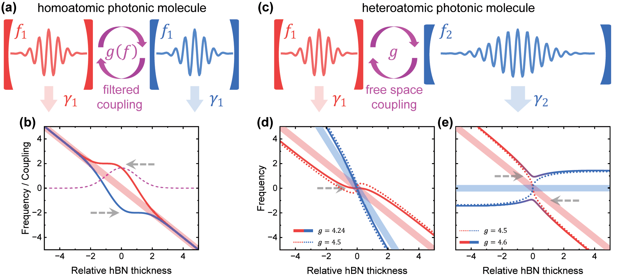
Coupled mode theory. (a) Schematic of the homoatomic photonic molecule. Two cavities have the same frequency f1 and loss rate γ1. A frequency-dependent (filter) coupling between them is used to achieve a parameter regime having a robust eigenfrequency. (b) The light line represents the bare frequency f1. The purple line is the frequency-dependent coupling strength g(f). The solid lines represent the eigenfrequencies of the molecule. (c) Schematic of the heteroatomic molecule. Two cavities have different frequencies f1(2) and loss rates γ1(2). (d)–(e) The light lines represent the bare frequencies f1(2). The dotted lines are the eigenfrequencies at the diabolical point (threshold between weak and strong coupling). Solid lines represent the eigenfrequencies of the molecules having a robust regime. Gray dashed arrows in (b) and (d)–(e) denote the position of robust eigenfrequencies (region with vanishing slope).
The homoatomic molecule depicted schematically in Figure 1(a) requires a filtered photonic mode coupling. In contrast, direct coupling in the free space between two cavities is much easier to achieve from a technological perspective. In this case, the coupling strength g is determined bhy the separation of the two cavities, whilst the frequency dependence is not significant. As discussed above, if g is nearly constant, the eigenfrequencies f± of a homoatomic molecule will still vary linearly. Therefore, we construct heteroatomic molecules to achieve nonlinear f± in the free space, as schematically shown in Figure 1(c). The cavity C1 (red) is identical to that used in the homoatomic case which has f1 = −thBN and γ1 = 2. We set the cavity C2 (blue) as a lower Q-factor with the larger loss rate γ2 = 20. Equations (1) and (2) indicate that, when the coupling strength exceeds the decay rate g > Δγ/4, the molecule operates in the strong coupling regime with a splitting. In contrast, in the weak coupling regime g < Δγ/4, it operates without an anticrossing [40]. Moreover, the eigenfrequencies f± exhibit strong non-linearity and non-monotonicity around the diabolical point g = Δγ/4, the degenerate state at the threshold between weak and strong coupling [41, 42].
Figure 1(d) shows the calculated eigenfrequencies with f2 = −2thBN, meaning that the low-Q cavity C2 shifts more rapidly than the high-Q cavity C1 with the hBN thickness. The light lines (red and blue) are the bare frequencies f1(2), whilst the dotted lines (red and blue) are the eigenfrequencies f± at the diabolical point g = 4.5. As shown, the high-Q mode (red dotted line) exhibits strong non-linearity and non-monotonicity. In contrast, the solid lines (red and blue) are the case of g = 4.24 which is slightly below the diabolical point. Since the system is in a weak coupling regime, the superposition of the two cavities is not significant, and thereby, cavity C1 dominates in the spatial profile of the high-Q mode. Moreover, in this case, the first-order (linear slope) and second-order derivative of the high-Q mode frequency (red line) to thBN are both zero at the resonance thBN = 0, thus generating robust eigenfrequency regimes denoted by the gray dashed arrows in the figure.
Figure 1(e) presents the results with f2 = 0, which means the low-Q cavity C2 is not an hBN cavity. The light lines (red and blue) are the bare frequencies f1(2), whereas the dotted lines (red and blue) represent the situation at the diabolical point g = 4.5. For f2 = 0, we cannot use a g which is slightly below the diabolical point, because the high-Q mode (red) blue shifts at thBN < 0 whilst redshifts at thBN > 0. As a result, the indeterminacy (slope) around the resonance is enhanced rather than suppressed. In contrast, the robust eigenfrequencies are achieved by g slightly above the diabolical point, as shown by the case of g = 4.6 (solid red–blue lines) in Figure 1(e). In this case, the eigenfrequencies exhibits strong non-monotonicities, which provides the minima and maxima points with zero linear slopes. Meanwhile, the mixture of red and blue color around the resonance thBN = 0 denotes that the eigenstates are the superposition of modes from both two cavities, which means their spatial profile still involves cavity C1, the one we want to suppress the indeterminacy. Therefore, the case of g = 4.6 in Figure 1(e) is also valid to achieve robust resonance frequencies.
3 2D-material cavities and mode couplings
The excitonic properties of 2D semiconductors are degraded when placed into an inhomogeneous environment such as dielectric disorder [25]. In this case, the exciton linewidth is broadened, and some novel single-photon emitters will be suppressed [43, 44]. Therefore, 2D heterostructures with full hBN encapsulation is necessary to achieve the pristine excitonic and optical qualities [23, 24]. Nowadays, the most common method used to build 2D heterostructures and integrate them into a nanocavity is dry viscoelastic stamping followed by transfer on top of pre-fabricated photonic cavities [45–48]. However, the attachment limits the cavity-matter overlap and decreases the cavity Q-factor. Another way is to directly fabricate nanophotonic structures using hBN [28, 29], with the problem that hBN cannot readily be etched [49]. To solve these problems, we recently proposed a hybrid nanobeam cavity design [31, 32] that integrates hBN into nanocavities whilst avoiding etching of nanostructures into hBN layers. As presented in Figure 2(a), all nanoscale trenches are etched in Si3N4 using mature fabrication technologies, whilst the hBN layer is not perforated. Such nanocavities have been experimentally demonstrated to simultaneously achieve pristine excitonic quality, high Q-factor and large cavity-matter overlap, providing an ideal platform to explore the fundamental physics of 2D materials and their light–matter interaction in nanophotonic systems [50–52].
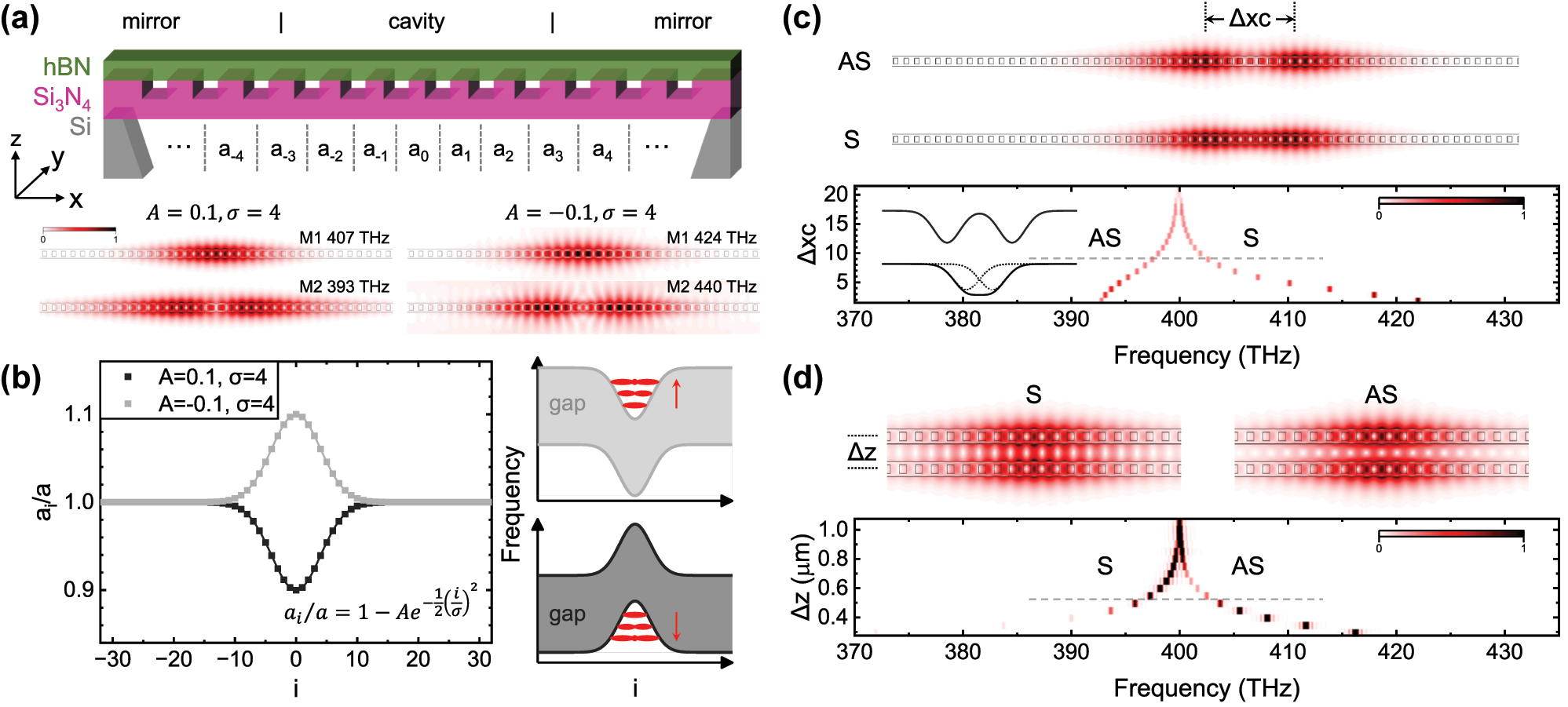
Fundamental properties of a single cavity and the molecule. (a) Schematic of the hBN/Si3N4 nanobeam cavity and typical photonic modes for a cavity with A > 0 (left) or A < 0 (right). (b) The photonic confinement is achieved by varying the periodicity at the center, defined by the Gaussian function with A and σ. Insets show that determined by if A is negative or positive, the confinement is concave or convex. (c) Coupling two cavities within one nanobeam or (d) two nanobeams. Δxc in (c) and Δz in (d) is the distance between the center point of two cavities. Gray lines and insets in the spectra in (c) and (d) denote that the coupled mode theory is valid for a relatively large distance, i.e., Δxc > 8 in (c) and Δz > 500 nm in (d). In contrast, if the distance is too small, the two-photon confinements merge into one.
As presented in Figure 2(b), the cavity photonic confinement is formed by locally chirping the photonic crystal periodicity around the center point. The distance between nanoscale trenches (periodicity) follows a Gaussian profile
where a i is the ith distance schematically shown in Figure 2(a), a is the lattice constant, and A, σ defines the Gaussian profile. We fix the nanoscale trenches with the length h x = 120 nm, depth h z = 150 nm and lattice constant a = 270 nm, whilst the Si3N4 has a thickness of 200 nm. The designed hBN thickness thBN is 50 nm. At the bottom of Figure 2(a), we present typical modes for two cavities with A = 0.1, σ = 4 and A = −0.1, σ = 4 calculated using 2D FDTD. For A = 0.1, σ = 4, the fundamental mode M1 is at 407 THz with a Q-factor of 4.8 × 10⁶ and the second mode M2 is at 393 THz with a Q-factor of 1.8 × 10⁴. For A = −0.1, σ = 4, the fundamental mode M1 is at 424 THz with a Q-factor of 5.9 × 10³ and the second mode M2 is at 440 THz with a Q-factor of 820. Since the refractive index of hBN is not well established [53, 54], we use a fixed value of 2.0 for both hBN and Si3N4, while the mesh size used was 10 nm, providing a precision better than 0.01 %.
We observe that for A > 0, the frequency of mode M2 is lower than M1, while it is higher when A < 0. This different mode frequency sequence arises from the different photonic bandgap as presented schematically in Figure 2(b). For A < 0, the periodicity at the center is increased. The larger periodicity means a longer wavelength (lower frequency), thus the bandgap confinement is concave at the center. Thereby, the higher order mode (larger mode volume) has a higher frequency. Vice versa, for A > 0 the bandgap confinement is convex, and thereby, the higher order mode has a lower frequency. The cavity with A < 0 has a lower Q-factor, and the field mainly distributes in the air gaps. Therefore, the convex bandgap confinement is usually used in 1D nanobeam photonic crystal cavities [47, 48].
The photonic molecule can be constructed by coupling two cavities within one nanobeam or in two separated nanobeams. For the case within one nanobeam, we define the periodicity profile as
where the center point of the two cavities are at xc1(2) with the Gaussian profile A1(2) and σ1(2). The coupling strength is controlled by the distance between them Δxc = xc1 − xc2, as shown in Figure 2(c). For the case with two separated nanobeams, we set xc1 = xc2 = 0, and the coupling strength is controlled by the distance between two nanobeams Δz as shown in Figure 2(d). In Figure 2(c) and (d) we present the distance-dependent spectra calculated using 2D FDTD, in the case of molecules with one or two nanobeams, respectively. A homoatomic profile A1(2) = 0.2 and σ1(2) = 2 are used. The symmetric (S) and antisymmetric (AS) modes have opposite frequency sequences in the two cases since the bandgap confinement in the x direction along the nanobeam is convex for A > 0 whilst concave in the z direction.
The S and AS modes of the photonic molecule can be generally described by the coupled mode theory in Eqs. (1) and (2), but it is not strict. For example, it predicts the homoatomic molecule with f1 = f2 to have a symmetric splitting with eigenfrequencies f± = f1 ± g and the loss rate of S and AS modes remains γ1. However, in the FDTD calculation results, e.g., the case in the upper panel of Figure 2(c) which corresponds to Δxc = 9, the Q-factor is 1.2 × 10⁵ for AS mode while 5.3 × 10⁵ for S mode. This is due to the limitations of the coupled mode theory. Firstly, in Eqs. (1) and (2) we use a real g to describe the coupling, but in reality, this term could also involve an imaginary part which results in a non-Hermitian system [36, 55]. The imaginary coupling results in different loss rates of S and AS modes. Secondly, the coupled mode theory is valid for individual cavities that couple to each other through the evanescent field. When the distance between the two cavities is large, i.e., Δxc > 8 in Figure 2(c) and Δz > 500 nm in (d), we observe a nearly symmetric splitting which indicates that the two cavities are approximately individual. In contrast, the splitting becomes asymmetric as the distance decreases, because the two confinements merge into one and the two cavities are no longer individual. The comparison between individual and non-individual cases is schematically presented in the inset of Figure 2(c). Nonetheless, the calculation results in Figure 2(c) and (d) reveal that for both types of the photonic molecule, when the coupling strength g is smaller than 2.5 (corresponding to Δxc = 9 or Δz = 550 nm), the eigenfrequencies split symmetrically thus can be well described by the coupled mode theory.
Before exploring the nonlinear eigenfrequencies for photonic molecules, we first study the hBN thickness dependence of the bare frequency of a single cavity. Usually, apparent optical contrast is used to quickly identify the thickness of hBN flakes [56], but the error of this method remains ± several layers, corresponding to a thickness of ∼2 nm. In Figure 3(a) we present the hBN thickness (thBN) dependence of cavity modes calculated using 2D FDTD. For several different values of A and σ, the cavity mode exhibits a similar frequency shift slope of −0.6 THz/nm. This means that in the 2D space, it is difficult to have two cavities with remarkably different thBN dependent frequency shifts. Therefore, to achieve the bare frequencies as predicted in Figure 1(d) of the two cavities, we extend the system to 3D space. The dry etching of hBN normally has an etching angle that can be optimized by the recipe [49], but it is difficult to make it completely vertical. Due to the non-vertical characteristic, the hBN thickness thBN also impacts the nanobeam width
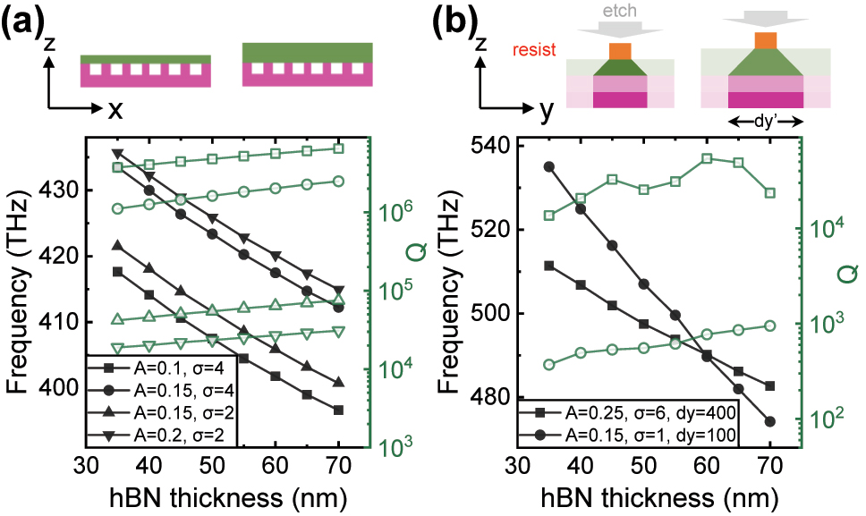
thBN dependence of a single cavity. (a) 2D FDTD calculation. For several values of A and σ, the cavity mode exhibits a similar linear frequency shift. (b) 3D FDTD calculation. Due to the etching angle of hBN, thBN also affects the actual nanobeam width dy′. Thereby, we can control the frequency shift slope by the designed nanobeam width dy.
The 2D FDTD results in Figure 2(c) and (d) reveal that the coupling strength of the photonic molecule can be controlled by the distance in x and z direction. Similarly, the coupling can also be controlled by the distance in y direction when we extend the system to 3D space [31]. The 2D FDTD is a valid approximation of the 3D system, when the two cavities have the same nanobeam width d y in the y direction. Based on the results in Figure 3, we obtain that different d y in 3D space is only necessary to achieve remarkably different shifts of bare frequencies, which corresponds to Figure 1(d). In contrast, uniform d y is enough to achieve the bare frequencies in Figure 1(b) and (e). Therefore, we use 2D FDTD to demonstrate the robust eigenfrequencies for the cases of Figure 1(b) and (e) and 3D FDTD for the case of Figure 1(d). From simple to complex, we next first show the case of Figure 1(e) in Figure 4, then the case of Figure 1(d) in Figure 5 and finally discuss the case of Figure 1(b) in Figure 6.
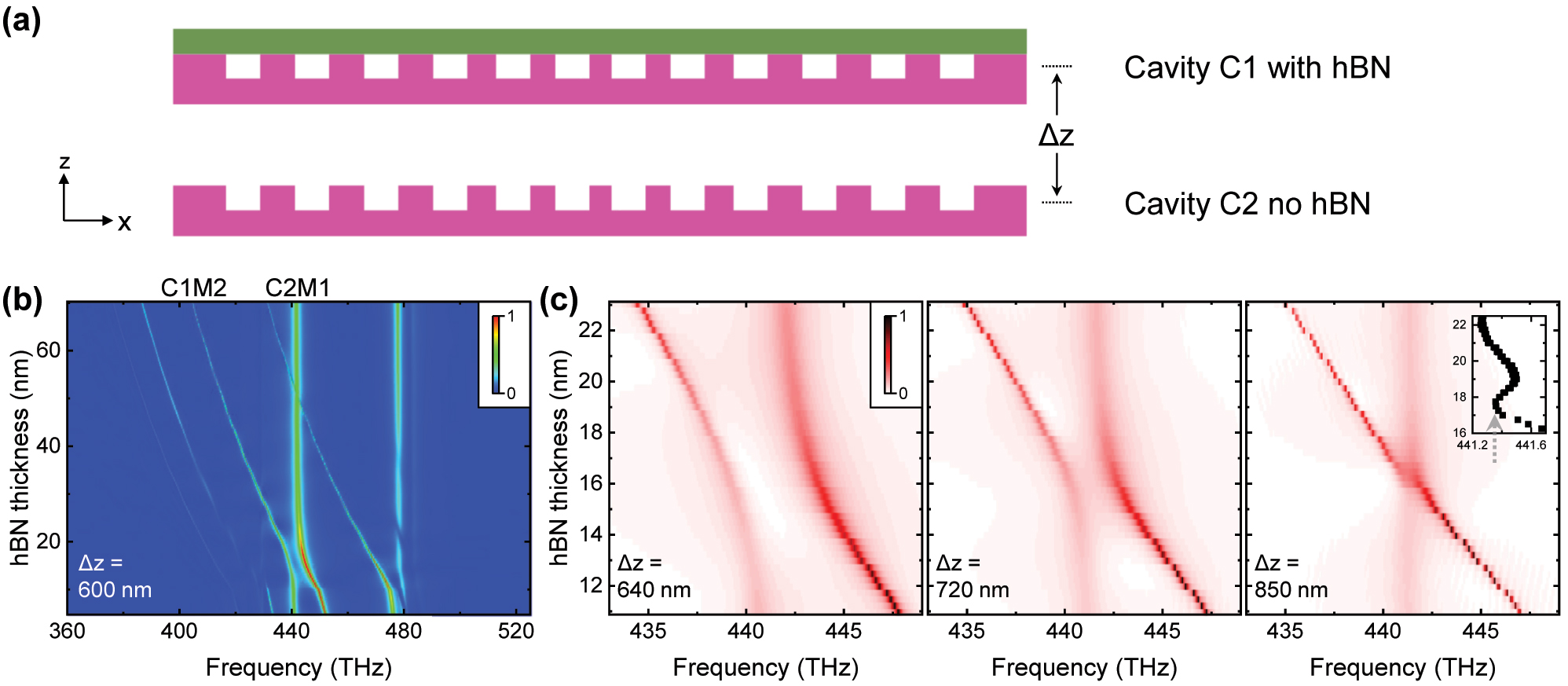
Robust eigenfrequency achieved by heteroatomic molecule involving one hBN cavity. (a) Schematic of the photonic molecule for which one cavity is with hBN whilst the other is not. The coupling between two cavities is controlled by the distance Δz. (b) Calculated spectra for the distance Δz = 600 nm. (c) By increasing Δz, robust eigenfrequencies are observed at Δz = 850 nm. Inset shows the frequency of AS mode which agrees well with the prediction in Figure 1(e).
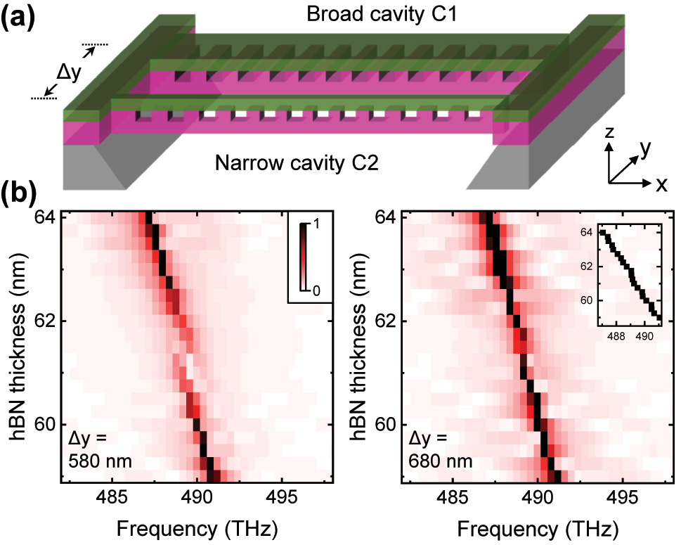
Robust eigenfrequency achieved by heteroatomic molecule consisting of two hBN cavities. (a) Schematic of the photonic molecule by coupling the two cavities in Figure 3(b). (b) Calculated spectra with the distance Δy = 580 and 680 nm. Inset shows the frequency of high-Q mode at Δy = 680 nm, which agrees well to the prediction in Figure 1(d).
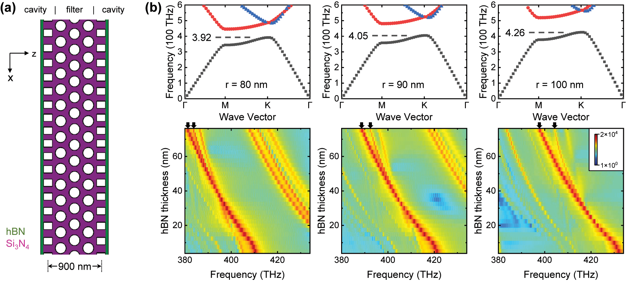
Exploring filtered coupling in homoatomic molecule. (a) Schematic of the photonic molecule with the filter coupler. (b) Upper panels are the bandstructure of the 2D hexagonal photonic crystal in the cases of different air hole radius r. Dashed lines denote the lower edge of the bandgap. The bottom panels are the corresponding spectra. Black arrows denote the split peaks. The splitting occurs above the threshold when its frequency reaches the photonic band shown in the upper panels.
4 Heteroatomic molecules
We firstly discuss the heteroatomic molecule comprising an hBN/Si3N4 hybrid cavity and a second cavity without hBN, corresponding to the case predicted in Figure 1(e). Here we approximate the photonic molecule in the xz 2D space as shown in Figure 4(a), and control the coupling g between the two cavities by varying the distance Δz. This approximation is of course not strict, but the key point, i.e., varying the distance between the two cavities to achieve a photonic molecule around the diabolical point, is the same for the real 3D structure and the 2D approximation.
We use A = 0.2, σ = 4 for the high-Q cavity C1 and A = −0.3, σ = 1 for the low-Q cavity C2. Since the coupled mode theory only applies to relatively large distance Δz > 500 nm (Figure 2(d)), we first calculate the hBN thickness thBN dependent spectra at Δz = 600 nm and present the result in Figure 4(b). The four sharp peaks shifting significantly with thBN are from the high-Q cavity C1, and the two broad peaks exhibiting slight shifts are from the low-Q cavity C2. As shown, the mode M2 of cavity C1 (C1M2) exhibits a clear anticrossing to the mode M1 of cavity C2 (C2M1). The mode C1M2 has a bare frequency of 415 THz and a Q-factor of 2.5 × 10⁴ at the designed thickness thBN = 50 nm, and the mode C2M1 has a bare frequency of 441 THz and a Q-factor of 350. Increasing the distance Δz results in a reduction of the coupling strength g between these two modes. As presented in Figure 4(c), the splitting at resonance decreases with increasing Δz, and the system finally reaches the state slightly above the diabolical point as predicted in Figure 1(e). The inset in Figure 4(c) shows that the resonance frequency of AS mode varies by 0.14 THz within the indeterminacy 2 nm of thBN (17 − 19 nm), one order of magnitude smaller than the case in a single cavity (1.2 THz).
As discussed in the context of Figure 3(b), the frequency shift slope of a single cavity can be controlled by varying the nanobeam width d y in 3D space. Therefore, we construct a photonic molecule based on these two cavities. Hereby, we use A = 0.25, σ = 4, d y = 400 nm for the high-Q cavity C1 and A = 0.15, σ = 1, d y = 100 nm for the low-Q cavity C2. The mode coupling is controlled by the distance Δy as schematically shown in Figure 5(a). In Figure 5(b) we present the spectra with different Δy calculated using 3D FDTD. The resonance point of the two cavities is at thBN = 61.5 nm, consistent with the bare frequencies of single cavities in Figure 3(b). When Δy = 580 nm, we observe a significant anticrossing indicating that the system is in the strong coupling regime. In contrast, when Δy = 680 nm, the coupling strength reduces and the anticrossing is suppressed. Around the resonance thBN = 61.5 nm, the thBN dependent frequency shift of the high-Q mode is suppressed, as presented in the inset in Figure 5(b). The 3D calculation results in Figure 5 agree well with the state slightly below the diabolical point predicted in Figure 1(d).
5 Homoatomic molecules
In Figure 1(b) we predict that the homoatomic molecule with a filtered mode coupling g(f) is another method to achieve nonlinear resonance frequency and improve the robustness to thBN. The optical filter is usually realized by integrating material with nonlinear absorption allowing only the photons at certain frequencies to pass. However, the simulation of such complex materials in the FDTD calculation is non-trivial and we qualitatively explore the homoatomic molecule using a frequency selective coupler. As discussed in the context of Figure 3, 2D FDTD is a valid approximation to describe the case of Figure 1(b), and thereby, we propose the nanophotonic device defined in the xz plane as presented in Figure 6(a). The two nanobeam cavities are located on each side, and an array of the 2D hexagonal photonic crystal lattice is in the middle. Only the photons within the photonic band of the hexagonal photonic crystal are transmitted and exchanged between the two cavities. Therefore, the hexagonal photonic crystal serves as a frequency-selective filter for the mode coupling.
We set A = 0.2, σ = 4 for the two nanobeam cavities. The lattice constant of the hexagonal photonic crystal is set as a h = 270 nm, and we vary the radius of the air holes r to control the photonic band. The calculated photonic bands are presented in the upper panels in Figure 6(b), and the dashed lines denote the lower edge of the bandgap. This value is 392, 405 and 426 THz for the radius r of 80, 90 and 100 nm, exhibiting a positive dependence as expected. The calculated thBN dependent spectra are presented in the bottom panels in Figure 6(b). Multiple peaks are observed because the nanophotonic structure in Figure 6(a) is very complex. Here we mainly focus on the peak with the largest intensity and its splitting, which are denoted by the black arrows on top of the spectra. The splitting occurs when the hBN thickness thBN exceeds a threshold. Moreover, this threshold in the cases of r = 80, 90 and 100 nm corresponds to the frequency of 392, 402 and 415 THz, respectively. These values are consistent with the band of the hexagonal photonic crystal denoted in the upper panels in Figure 6(b), indicating that the hexagonal photonic crystal is a valid filter for this photonic molecule.
We note that the nanophotonic structure in Figure 6(a) is a simple example to qualitatively explore the filtered coupling. We use the distance of 900 nm because larger distance will suppress the coupling into the weak regime as shown in Figure 2(d). As such, the hexagonal photonic crystal has only three rows of air holes, which is not enough for a highly efficient filter. These limitations result in the relatively weak non-linearity, i.e., the thBN dependent shift of the splitting peak is reduced but not enough to obtain a robust (zero linear slope) resonance frequency. A potential optimization approach is introducing Δxc between the two nanobeam cavities. In this case, we can control (through Δxc) the wave vector direction of the photons that exchange between the two cavities, and match the wave vector to some points in the Γ−M−K−Γ photonic band. Thereby, the hexagonal photonic crystal will not only filter the frequency but also the wave vector, and thereby, the efficiency will be improved.
6 Conclusions
In summary, we have demonstrated that the nonlinearity of the mode coupling in the photonic molecules results in coupled mode eigenfrequencies that are robust to the thickness of 2D heterostructure. Although atomically thin semiconductors have well-defined emission energies compared to the random energy of traditional quantum dots, the indeterminate thickness of their hBN encapsulation leads to indeterminate cavity resonance frequencies. For a single cavity, the frequency shift of 0.6 THz/nm is obtained in the 2D FDTD calculations, and a value of 1.7 THz/nm is obtained in the 3D calculations. By comparison, the linewidth of the free excitons in the atomically thin semiconductors such as monolayer transition metal dichalcogenides at low temperatures is ∼5 meV (1.2 THz) and that of the localized excitons is 0.1–0.2 meV (∼50 GHz). As a result, it is difficult to achieve the light–matter resonance directly in a single cavity, and complex external methods have to be used to control the detuning [31, 52]. Our results reveal that photonic molecules are capable of exhibiting thickness-independent resonance frequencies, thus having great potential in the 2D-material nanophotonics, especially the detuning sensitive applications such as lasing and exciton-photon polaritons.
Funding source: Munich Center for Quantum Science and Technology http://dx.doi.org/10.13039/501100021825
Award Identifier / Grant number: EXS-2089
Award Identifier / Grant number: EXS-2111
Funding source: China Scholarship Council
Award Identifier / Grant number: 202006280067
Funding source: Deutsche Forschungsgemeinschaft http://dx.doi.org/10.13039/501100001659
Award Identifier / Grant number: SPP-2244
Funding source: Alexander von Humboldt-Stiftung http://dx.doi.org/10.13039/100005156
Funding source: National Key Research and Development Program of China
Award Identifier / Grant number: 2021YFF0700402
Funding source: Fundamental Research Funds for the Central Universities
Funding source: National Science Fund for Distinguished Young Scholars
Award Identifier / Grant number: 52225507
-
Research funding: S. Y. and P. J. acknowledge support from the National Science Fund for Distinguished Young Scholars (No. 52225507), the National Key Research and Development Program of China (No. 2021YFF0700402), and the Fundamental Research Funds for the Central Universities. J. F., C. Q. and P. J. gratefully acknowledge the German Science Foundation (DFG) for financial support via grants SPP-2244, as well as the clusters of excellence MCQST (EXS-2111) and e-conversion (EXS-2089). C. Q. gratefully acknowledges the Alexander v. Humboldt foundation for financial support in the framework of their fellowship programme. P. J. acknowledges support from the China Scholarship Council (202006280067).
-
Author contributions: C. Q., J. F. and S. Y. conceived the project. P. J. and C. Q. performed the calculations. All authors discussed the results and wrote the manuscript.
-
Conflict of interest statement: Authors state no conflict of interest.
-
Data availability statement: The datasets generated during and/or analyzed during the current study are available from the corresponding authors on reasonable request.
References
[1] E. Yablonovitch, “Inhibited spontaneous emission in solid-state physics and electronics,” Phys. Rev. Lett., vol. 58, pp. 2059–2062, 1987. https://doi.org/10.1103/physrevlett.58.2059.Search in Google Scholar PubMed
[2] J. D. Joannopoulos, P. R. Villeneuve, and S. Fan, “Photonic crystals: putting a new twist on light,” Nature, vol. 386, pp. 143–149, 1997. https://doi.org/10.1038/386143a0.Search in Google Scholar
[3] J. Joannopoulos, S. Johnson, J. Winn, and R. Meade, Photonic Crystals: Molding the Flow of Light, 2nd ed. New Jersey, Princeton University Press, 2011.10.2307/j.ctvcm4gz9Search in Google Scholar
[4] P. Lodahl, S. Mahmoodian, and S. Stobbe, “Interfacing single photons and single quantum dots with photonic nanostructures,” Rev. Mod. Phys., vol. 87, pp. 347–400, 2015. https://doi.org/10.1103/revmodphys.87.347.Search in Google Scholar
[5] T. F. Krauss, R. M. D. L. Rue, and S. Brand, “Two-dimensional photonic-bandgap structures operating at near-infrared wavelengths,” Nature, vol. 383, pp. 699–702, 1996. https://doi.org/10.1038/383699a0.Search in Google Scholar
[6] C. P. Dietrich, A. Fiore, M. G. Thompson, M. Kamp, and S. Höfling, “Gaas integrated quantum photonics: towards compact and multi-functional quantum photonic integrated circuits,” Laser Photon. Rev., vol. 10, no. 6, pp. 870–894, 2016. https://doi.org/10.1002/lpor.201500321.Search in Google Scholar
[7] T. Asano and S. Noda, “Photonic crystal devices in silicon photonics,” Proc. IEEE, vol. 106, no. 12, pp. 2183–2195, 2018. https://doi.org/10.1109/jproc.2018.2853197.Search in Google Scholar
[8] Y. Akahane, T. Asano, B.-S. Song, and S. Noda, “High-q photonic nanocavity in a two-dimensional photonic crystal,” Nature, vol. 425, pp. 944–947, 2003. https://doi.org/10.1038/nature02063.Search in Google Scholar PubMed
[9] J. Sweet, B. Richards, J. Olitzky, et al.., “Gaas photonic crystal slab nanocavities: growth, fabrication, and quality factor,” Photon. Nanostruct., vol. 8, no. 1, pp. 1–6, 2010. https://doi.org/10.1016/j.photonics.2009.10.004.Search in Google Scholar
[10] B.-S. Song, S. Noda, T. Asano, and Y. Akahane, “Ultra-high-q photonic double-heterostructure nanocavity,” Nat. Mater., vol. 4, pp. 207–210, 2005. https://doi.org/10.1038/nmat1320.Search in Google Scholar
[11] T. Yoshie, A. Scherer, J. Hendrickson, et al.., “Vacuum rabi splitting with a single quantum dot in a photonic crystal nanocavity,” Nature, vol. 432, pp. 200–203, 2004. https://doi.org/10.1038/nature03119.Search in Google Scholar PubMed
[12] A. Kress, F. Hofbauer, N. Reinelt, et al.., “Manipulation of the spontaneous emission dynamics of quantum dots in two-dimensional photonic crystals,” Phys. Rev. B, vol. 71, p. 241304, 2005. https://doi.org/10.1103/physrevb.71.241304.Search in Google Scholar
[13] K. Hennessy, A. Badolato, M. Winger, et al.., “Quantum nature of a strongly coupled single quantum dot–cavity system,” Nature, vol. 445, pp. 896–899, 2007. https://doi.org/10.1038/nature05586.Search in Google Scholar PubMed
[14] H. Altug, D. Englund, and J. Vučković, “Ultrafast photonic crystal nanocavity laser,” Nat. Phys., vol. 2, pp. 484–488, 2006. https://doi.org/10.1038/nphys343.Search in Google Scholar
[15] H. Kim, R. Bose, T. C. Shen, G. S. Solomon, and E. Waks, “A quantum logic gate between a solid-state quantum bit and a photon,” Nat. Photonics, vol. 7, pp. 373–377, 2013. https://doi.org/10.1038/nphoton.2013.48.Search in Google Scholar
[16] Y. Ota, S. Iwamoto, N. Kumagai, and Y. Arakawa, “Spontaneous two-photon emission from a single quantum dot,” Phys. Rev. Lett., vol. 107, p. 233602, 2011. https://doi.org/10.1103/physrevlett.107.233602.Search in Google Scholar
[17] C. Qian, S. Wu, F. Song, et al.., “Two-photon rabi splitting in a coupled system of a nanocavity and exciton complexes,” Phys. Rev. Lett., vol. 120, p. 213901, 2018. https://doi.org/10.1103/physrevlett.120.213901.Search in Google Scholar PubMed
[18] S. Reitzenstein, S. Münch, P. Franeck, et al.., “Control of the strong light-matter interaction between an elongated in0.3ga0.7As quantum dot and a micropillar cavity using external magnetic fields,” Phys. Rev. Lett., vol. 103, p. 127401, 2009. https://doi.org/10.1103/physrevlett.103.127401.Search in Google Scholar
[19] A. Faraon, A. Majumdar, H. Kim, P. Petroff, and J. Vučković, “Fast electrical control of a quantum dot strongly coupled to a photonic-crystal cavity,” Phys. Rev. Lett., vol. 104, p. 047402, 2010. https://doi.org/10.1103/physrevlett.104.047402.Search in Google Scholar PubMed
[20] C. Qian, X. Xie, J. Yang, et al.., “Enhanced strong interaction between nanocavities and p-shell excitons beyond the dipole approximation,” Phys. Rev. Lett., vol. 122, p. 087401, 2019. https://doi.org/10.1103/physrevlett.122.087401.Search in Google Scholar
[21] U. Hohenester, A. Laucht, M. Kaniber, et al.., “Phonon-assisted transitions from quantum dot excitons to cavity photons,” Phys. Rev. B, vol. 80, p. 201311, 2009. https://doi.org/10.1103/physrevb.80.201311.Search in Google Scholar
[22] S. Sun, H. Kim, G. S. Solomon, and E. Waks, “Strain tuning of a quantum dot strongly coupled to a photonic crystal cavity,” Appl. Phys. Lett., vol. 103, p. 151102, 2013. https://doi.org/10.1063/1.4824712.Search in Google Scholar
[23] J. Wierzbowski, J. Klein, F. Sigger, et al.., “Direct exciton emission from atomically thin transition metal dichalcogenide heterostructures near the lifetime limit,” Sci. Rep., vol. 7, p. 12383, 2017. https://doi.org/10.1038/s41598-017-09739-4.Search in Google Scholar PubMed PubMed Central
[24] F. Cadiz, E. Courtade, C. Robert, et al.., “Excitonic linewidth approaching the homogeneous limit in mos2-based van der waals heterostructures,” Phys. Rev. X, vol. 7, p. 021026, 2017. https://doi.org/10.1103/physrevx.7.021026.Search in Google Scholar
[25] A. Raja, L. Waldecker, J. Zipfel, et al.., “Dielectric disorder in two-dimensional materials,” Nat. Nanotechnol., vol. 14, pp. 832–837, 2019. https://doi.org/10.1038/s41565-019-0520-0.Search in Google Scholar PubMed
[26] P. Ji, S. Yang, Y. Wang, et al.., “High-performance photodetector based on an interface engineering-assisted graphene/silicon Schottky junction,” Microsyst. Nanoeng., vol. 8, p. 9, 2022. https://doi.org/10.1038/s41378-021-00332-4.Search in Google Scholar PubMed PubMed Central
[27] J. Jang, M. Jeong, J. Lee, S. Kim, H. Yun, and J. Rho, “Planar optical cavities hybridized with low-dimensional light-emitting materials,” Adv. Mater., vol. 35, no. 4, p. 2203889, 2023. https://doi.org/10.1002/adma.202203889.Search in Google Scholar PubMed
[28] S. Kim, J. E. Fröch, J. Christian, et al.., “Photonic crystal cavities from hexagonal boron nitride,” Nat. Commun., vol. 9, p. 2623, 2018. https://doi.org/10.1038/s41467-018-05117-4.Search in Google Scholar PubMed PubMed Central
[29] J. E. Fröch, Y. Hwang, S. Kim, I. Aharonovich, and M. Toth, “Photonic nanostructures from hexagonal boron nitride,” Adv. Opt. Mater., vol. 7, no. 4, p. 1801344, 2019. https://doi.org/10.1002/adom.201801344.Search in Google Scholar
[30] N. Fang, D. Yamashita, S. Fujii, et al.., “Quantization of mode shifts in nanocavities integrated with atomically thin sheets,” Adv. Opt. Mater., vol. 10, no. 19, p. 2200538, 2022. https://doi.org/10.1002/adom.202200538.Search in Google Scholar
[31] C. Qian, V. Villafañe, P. Soubelet, et al.., “Nonlocal exciton-photon interactions in hybrid high-q beam nanocavities with encapsulated mos2 monolayers,” Phys. Rev. Lett., vol. 128, p. 237403, 2022. https://doi.org/10.1103/physrevlett.128.237403.Search in Google Scholar
[32] C. Qian, V. Villafañe, M. M. Petrić, P. Soubelet, A. V. Stier, and J. J. Finley, “Coupling of mos2 excitons with lattice phonons and cavity vibrational phonons in hybrid nanobeam cavities,” Phys. Rev. Lett., vol. 130, p. 126901, 2023. https://doi.org/10.1103/physrevlett.130.126901.Search in Google Scholar PubMed
[33] S. Vignolini, F. Riboli, F. Intonti, et al.., “Mode hybridization in photonic crystal molecules,” Appl. Phys. Lett., vol. 97, p. 063101, 2010. https://doi.org/10.1063/1.3475490.Search in Google Scholar
[34] F. Brossard, B. Reid, C. Chan, et al.., “Confocal microphotoluminescence mapping of coupled and detuned states in photonic molecules,” Opt. Express, vol. 21, pp. 16934–16945, 2013. https://doi.org/10.1364/oe.21.016934.Search in Google Scholar PubMed
[35] Y. Zhao, C. Qian, K. Qiu, Y. Gao, and X. Xu, “Ultrafast optical switching using photonic molecules in photonic crystal waveguides,” Opt. Express, vol. 23, pp. 9211–9220, 2015. https://doi.org/10.1364/oe.23.009211.Search in Google Scholar PubMed
[36] K. Liao, X. Hu, T. Gan, et al.., “Photonic molecule quantum optics,” Adv. Opt. Photon, vol. 12, pp. 60–134, 2020. https://doi.org/10.1364/aop.376739.Search in Google Scholar
[37] H. Haus and W. Huang, “Coupled-mode theory,” Proc. IEEE, vol. 79, no. 10, pp. 1505–1518, 1991. https://doi.org/10.1109/5.104225.Search in Google Scholar
[38] M. Qiu, M. Mulot, M. Swillo, et al.., “Photonic crystal optical filter based on contra-directional waveguide coupling,” Appl. Phys. Lett., vol. 83, pp. 5121–5123, 2003. https://doi.org/10.1063/1.1634373.Search in Google Scholar
[39] M. Seifouri, V. Fallahi, and S. Olyaee, “Ultra-high-q optical filter based on photonic crystal ring resonator,” Photon. Netw. Commun., vol. 35, pp. 225–230, 2018. https://doi.org/10.1007/s11107-017-0732-x.Search in Google Scholar
[40] B. Peng, Ş. K. Özdemir, J. Zhu, and L. Yang, “Photonic molecules formed by coupled hybrid resonators,” Opt. Lett., vol. 37, pp. 3435–3437, 2012. https://doi.org/10.1364/ol.37.003435.Search in Google Scholar
[41] F. Keck, H. J. Korsch, and S. Mossmann, “Unfolding a diabolic point: a generalized crossing scenario,” J. Phys. A: Math. Gen., vol. 36, p. 2125, 2003. https://doi.org/10.1088/0305-4470/36/8/310.Search in Google Scholar
[42] J. Yang, C. Qian, X. Xie, et al.., “Diabolical points in coupled active cavities with quantum emitters,” Light Sci. Appl., vol. 9, p. 6, 2020. https://doi.org/10.1038/s41377-020-0244-9.Search in Google Scholar PubMed PubMed Central
[43] J. Klein, M. Lorke, M. Florian, et al.., “Site-selectively generated photon emitters in monolayer mos2 via local helium ion irradiation,” Nat. Commun., vol. 10, p. 2755, 2019. https://doi.org/10.1038/s41467-019-10632-z.Search in Google Scholar PubMed PubMed Central
[44] Y. Liu, C. Zeng, J. Yu, et al.., “Moiré superlattices and related moiré excitons in twisted van der waals heterostructures,” Chem. Soc. Rev., vol. 50, pp. 6401–6422, 2021. https://doi.org/10.1039/d0cs01002b.Search in Google Scholar PubMed
[45] S. Wu, S. Buckley, J. R. Schaibley, et al.., “Monolayer semiconductor nanocavity lasers with ultralow thresholds,” Nature, vol. 520, pp. 69–72, 2015. https://doi.org/10.1038/nature14290.Search in Google Scholar PubMed
[46] Y. Ye, Z. J. Wong, X. Lu, et al.., “Monolayer excitonic laser,” Nat. Photonics, vol. 9, pp. 733–737, 2015. https://doi.org/10.1038/nphoton.2015.197.Search in Google Scholar
[47] Y. Li, J. Zhang, D. Huang, et al.., “Room-temperature continuous-wave lasing from monolayer molybdenum ditelluride integrated with a silicon nanobeam cavity,” Nat. Nanotechnol., vol. 12, pp. 987–992, 2017. https://doi.org/10.1038/nnano.2017.128.Search in Google Scholar PubMed
[48] D. Rosser, D. Gerace, Y. Chen, et al.., “Dispersive coupling between mose2 and an integrated zero-dimensional nanocavity,” Opt. Mater. Express, vol. 12, pp. 59–72, 2022. https://doi.org/10.1364/ome.443536.Search in Google Scholar
[49] S. Grenadier, J. Li, J. Lin, and H. Jiang, “Dry etching techniques for active devices based on hexagonal boron nitride epilayers,” J. Vac. Sci. Technol. A, vol. 31, p. 061517, 2013. https://doi.org/10.1116/1.4826363.Search in Google Scholar
[50] C. Qian, V. Villafañe, M. Schalk, et al.., “Unveiling the zero-phonon line of the boron vacancy center by cavity-enhanced emission,” Nano Lett., vol. 22, no. 13, pp. 5137–5142, 2022. https://doi.org/10.1021/acs.nanolett.2c00739.Search in Google Scholar PubMed
[51] C. Qian, V. Villafañe, M. Schalk, et al.., “Emitter-optomechanical interaction in ultra-high-q hbn nanocavities,” arXiv:2210.00150, 2022.Search in Google Scholar
[52] C. Qian, M. Troue, J. Figueiredo, et al.., “Lasing of moiré trapped mose2/wse2 interlayer excitons coupled to a nanocavity,” arXiv:2302.07046, 2023.Search in Google Scholar
[53] S.-Y. Lee, T.-Y. Jeong, S. Jung, and K.-J. Yee, “Refractive index dispersion of hexagonal boron nitride in the visible and near-infrared,” Phys. Status Solidi B, vol. 256, no. 6, p. 1800417, 2019. https://doi.org/10.1002/pssb.201800417.Search in Google Scholar
[54] Y. Rah, Y. Jin, S. Kim, and K. Yu, “Optical analysis of the refractive index and birefringence of hexagonal boron nitride from the visible to near-infrared,” Opt. Lett., vol. 44, pp. 3797–3800, 2019. https://doi.org/10.1364/ol.44.003797.Search in Google Scholar PubMed
[55] K. Takata, N. Roberts, A. Shinya, and M. Notomi, “Imaginary couplings in non-hermitian coupled-mode theory: effects on exceptional points of optical resonators,” Phys. Rev. A, vol. 105, p. 013523, 2022. https://doi.org/10.1103/physreva.105.013523.Search in Google Scholar
[56] D. Golla, K. Chattrakun, K. Watanabe, T. Taniguchi, B. J. LeRoy, and A. Sandhu, “Optical thickness determination of hexagonal boron nitride flakes,” Appl. Phys. Lett., vol. 102, p. 161906, 2013. https://doi.org/10.1063/1.4803041.Search in Google Scholar
© 2023 the author(s), published by De Gruyter, Berlin/Boston
This work is licensed under the Creative Commons Attribution 4.0 International License.
Articles in the same Issue
- Frontmatter
- Research Articles
- Broadband synchronization of ultrafast pulse generation with double-walled carbon nanotubes
- Noncontractible loop states from a partially flat band in a photonic borophene lattice
- Experimental investigation of a near-field focusing performance of the IP-Dip polymer based 2D and 3D Fresnel zone plate geometries fabricated using 3D laser lithography coated with hyperbolic dispersion surface layered metamaterial
- 100-Gbps per-channel all-optical wavelength conversion without pre-amplifiers based on an integrated nanophotonic platform
- Multi-height metasurface for wavefront manipulation fabricated by direct laser writing lithography
- Enabling infinite Q factors in absorbing optical systems
- Erbium emitters in commercially fabricated nanophotonic silicon waveguides
- Four-dimensional experimental characterization of partially coherent light using incoherent modal decomposition
- Fine-tuning biexcitons-plasmon coherent states in a single nanocavity
- Möbius edge band and Weyl-like semimetal flat-band in topological photonic waveguide array by synthetic gauge flux
- Dual-band optical collimator based on deep-learning designed, fabrication-friendly metasurfaces
- Thickness insensitive nanocavities for 2D heterostructures using photonic molecules
- Beam-steering metasurfaces assisted coherent optical wireless multichannel communication system
- Asymmetric metasurface photodetectors for single-shot quantitative phase imaging
- Room-temperature unidirectional routing of valley excitons of monolayer WSe2 via plasmonic near-field interference in symmetric nano-slits