Colloidal self-assembly based ultrathin metasurface for perfect absorption across the entire visible spectrum
-
Jiayi Jiang
 and
Jianwen Dong
and
Jianwen Dong


Abstract
Perfect absorption over the entire visible spectrum can create a dark background for acquiring images with high contrast and improved resolution, which is crucial for various applications such as medical imaging, biological detection, and industrial non-destructive testing. The broadband absorption is desired to be achieved in an ultrathin structure for low noise as well as high integration. Here, we experimentally demonstrate a metasurface broadband perfect absorber with an ultrathin thickness of 148 nm and a large area of ∼10 cm2. Such a metasurface, with more than 97% absorption in the wavelength range from 400 to 800 nm, is composed of chromium nanodisk hexagonal array deposited on a chromium substrate with a silica spacer. A self-assembly based colloidal lithography nanofabrication method is developed for the scalable fabrication of the proposed nanostructure. We attribute the broadband absorption to the spectrally overlapped Fabry–Perot resonance, surface plasmon polariton, and localized surface plasmon resonances. Our results offer a novel approach to wafer-scale and low-cost manufacturing of absorption-based devices for applications such as high-contrast imaging and optical modulation.
1 Introduction
Dark-field photography is an important approach to acquire high contrast images for showing off the smooth curves of translucent or transparent objects. As an efficient imaging technique, it has been widely employed in medical and biological imaging, industrial non-destructive testing and security screening [1–3]. Through building a solid black background, dark-field photography can make observers see surface textures that otherwise be hidden using standard bright field. A direct and simple way to realize the dark background is using a broadband perfect absorber to eliminate the undesirable reflected or scattered light. The key criteria to assess the performance of such an absorber include the absorption strength in the visible region, as well as the volume of absorbing material. It is desirable to simultaneously possess high absorption intensity in the entire visible spectrum for generating high-contrast images, and thin material thickness for reducing noise [4, 5].
Metasurface is emerging as a promising candidate for broadband light absorber due to its unique and tailorable electromagnetic properties. Metasurfaces with nanoforest structures, such as carbon nanotubes or metal nanowires, can achieve broadband strong absorption by means of multilevel hybridized plasmon resonances and cavity mode resonances inside the hybrid nanoforest [6–9]. However, their large thickness (tens to hundreds of micrometres) impedes device integration and will cause relatively high intrinsic noise. Thin metasurface absorbers, which adopt metal-insulator-metal (MIM) configuration with subwavelength resonators, were recently extended to be broadband by using sophisticated schemes for blending resonant frequencies of individual resonating elements [10–17]. These complex nanostructures were fabricated predominantly by top-down lithography such as focused ion beam (FIB) milling and electron beam lithography (EBL), with inherent limitations on production throughput, available area, fabrication cost, and scalability [18]. Self-assembly based nanofabrication can provide a low-cost way to realize wafer-scale metasurfaces. Randomly dispersed [19, 20] or hexagonal densely arranged [21, 22] nanoparticles, combined with bottom layered substrate or upper deposited film, can lead to broadband perfect absorption [23, 24]. However, their structure thickness is larger than the diameter of the assembled nanoparticles, which makes it difficult to achieve ultrathin broadband absorbers.
Here, we demonstrate a broadband, polarization-independent ultrathin metasurface absorber with high feasibility for practical applications. Through the combined effect of Fabry–Perot resonance and surface plasmon resonances, the 148 nm-thick absorber, consisting of a chromium (Cr) nanodisk array, a silica (SiO2) spacer, and a Cr substrate, exhibits nearly perfect absorption in the entire visible spectrum. Our ultrathin device is promising for integrated, large-scale applications that require strong absorption in the visible region such as high-contrast imaging and optical modulation. In addition, we develop a self-assembled based nanofabrication method, using self-assembled colloidal nanoparticles as a mask followed by oxygen plasma etching and magnetron sputtering, to experimentally realize large-area (centimeter-scale) samples of the proposed broadband absorbers. Without any high-cost lithography (such as FIB, EBL, etc.), our cost-effective and scalable fabrication method provides an efficient way to high-throughput manufacturing of other nanophotonic structures and devices.
2 Design and fabrication
2.1 Structure design
The schematic of the proposed metasurface absorber is shown in Figure 1(a). Such a structure can be seen as a MIM stacked system. The top layer is composed of periodic chromium (Cr) nanodisk array with diameter D, height h, and period P, which is the core layer of the absorber, so that all incident electromagnetic wave energy enters the structure. The middle layer is a SiO2 dielectric spacer layer with the thicknesses t, where the incident electromagnetic wave is consumed. The bottom layer is metal chromium film with a thickness H. The optical constants of Cr and SiO2 are measured by the Cr and SiO2 films prepared by magnetron sputtering. Figure 1(b) shows the measured refractive indices of Cr and SiO2 using an ellipsometer. Solid and dashed lines are, respectively, the refractive index n and the extinction coefficient k at different wavelengths.
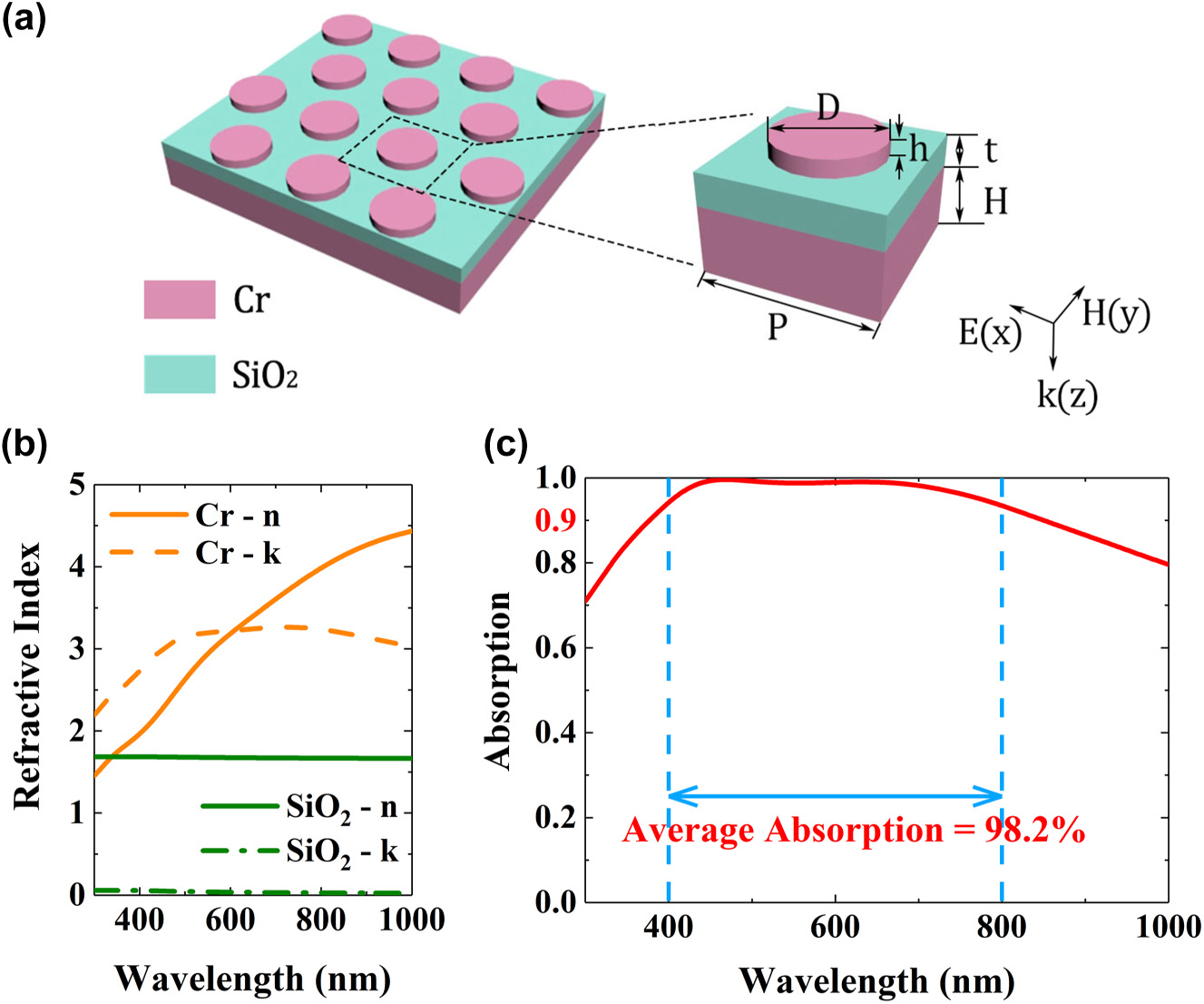
Design of broadband metasurface absorber. (a) Schematic of the broadband metasurface absorber. (b) Real and imaginary parts of the refractive indices of Cr and SiO2 measured from spectroscopic ellipsometry. (c) Simulated absorption spectrum of the metasurface absorber with P = 300 nm, D = 160 nm, h = 20 nm, t = 58 nm, and H = 70 nm.
We perform the finite-difference time-domain (FDTD) simulation using the measured refractive indices to investigate the performance of the metasurface absorber with P = 300 nm, D = 160 nm, h = 20 nm, t = 58 nm, and H = 70 nm. The absorption is calculated by A(λ) = 1 − R(λ) − T(λ), where R(λ) denotes reflectance and R(λ) denotes transmittance. Assume that the thickness of the bottom Cr layer is much larger than the penetration depth so that the incident light is blocked and the transmission is zero (T(λ) = 0). The absorption spectrum of the metasurface absorber is shown in Figure 1(c). It is seen that a near-perfect absorption band covers the entire visible light region and it has an average absorption rate 98.2% from 400 to 800 nm.
2.2 Experimental section and results
The proposed metasurface absorber is fabricated via a self-assembly based colloidal lithography method [25]. The fabrication scheme is shown in Figure 2.
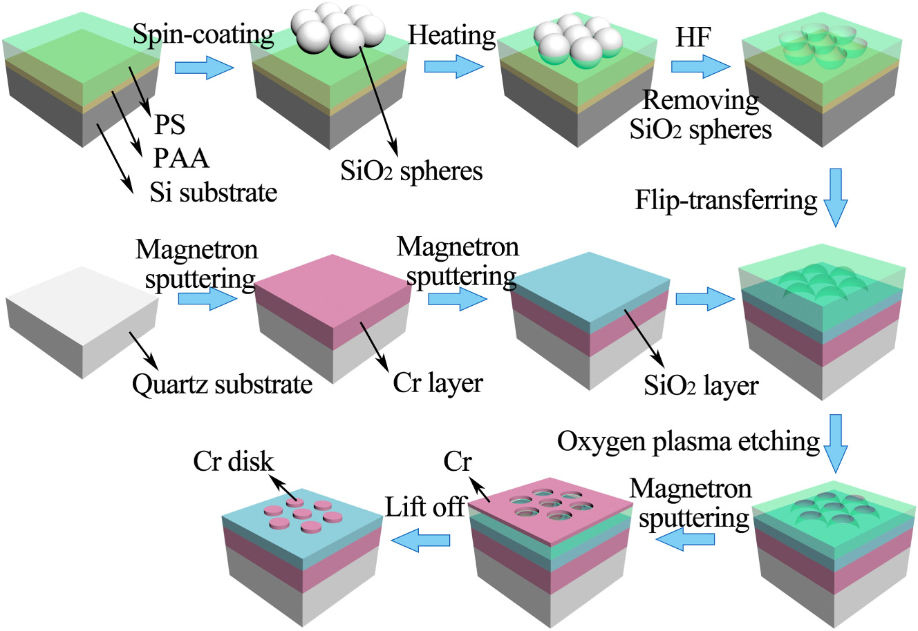
Scalable self-assembled-based fabrication scheme of the proposed metasurface absorber.
First, a cleaned quartz substrate is deposited, in turn, with a 120 nm-thick Cr film and a 58 nm-thick SiO2 film through magnetron sputtering. When the vacuum of the chamber is lower than 1.3 × 10⁻⁵ Pa, argon (Ar, pure 99.999%) is pumped into the chamber and works as glow gas. The Cr film is deposited with RF power of 50 W and pressure of 2.5 × 10⁻² Pa, and the SiO2 film is deposited with RF power of 120 W and pressure of 2.2 × 10⁻² Pa. The Cr/SiO2 structure is regarded as the substrate of the visible light metasurface absorber.
Second, the mask was fabricated as follows: a cleaned silicon substrate is spin coated, in turn, with a layer of sacrificial polyacrylic acid (PAA, 3 wt%) film at 1000 rpm for 37 s and the toluene solution of polystyrene (PS, 1.7 wt%) film at 2000 rpm for 37 s. Next, the hydrophilicity of the PS surface modification is made by oxygen plasma etching at the oxygen flow 6 sccm and the power 80 w for 40 s. Then, SiO2 solution with a diameter of 300 nm and a concentration of 20% is spin coated on the PS film at 300 rpm for 5 s and at 600 rpm for 35 s. A large-area, short-range orderly hexagonal close-packed SiO2 microsphere array is formed, as shown in Figure 3(a). Next, we place the sample on a heating stage at 120 °C for 4.5 min, so that the SiO2 microspheres are embedded into the PS film. Then, the sample is immersed in diluted hydrofluoric acid (HF) solution for 20 min in order to remove the SiO2 microsphere, forming a periodically arranged honeycomb array, as shown in Figure 3(b). The depth of the SiO2 microspheres embedded into the PS film depends on the heating time. However, the heating time should not be too long so that the SiO2 microspheres will not penetrate the PS film. Then, the sample is immersed in distilled water, and the PAA film is dissolved to separate the PS film from the silicon wafer. The PS film is floating on the water.
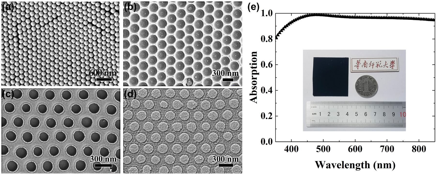
Structural characterization and measured spectrum. Scanning electron microscope (SEM) images of (a) hexagonal close-packed SiO2 nanosphere array, (b) hemispherical dimple honeycomb array in the PS film, (c) nanopore array in the PS film, and (d) periodic Cr nanodisk array. (e) Measured absorption spectrum of the absorber sample. The inset shows the camera image of the sample.
Third, the PS film is flip-transferred to the pre-fabricated Cr/SiO2 substrate of the metasurface absorber. Then, the PS film is gradually etched in a downward direction by oxygen plasma etching to obtain a periodic nanopore array, as shown in Figure 3(c). The diameter of the nanopore is determined by the etching time.
Finally, a Cr film of 20 nm-thick is deposited on the nanopore template by magnetron sputtering. After the lift-off process to remove the PS template with chlorobenzene, the periodic array of Cr nanodisk is fabricated, as shown in Figure 3(d). It is seen that the Cr nanodisk array has good symmetry, the ring traces on the surface are a small amount of residual PS film.
To characterize the fabricated metasurface absorbers, we use Maya 2000 Pro VIS-NIR spectrometer to measure the absorption of the samples. Figure 3(e) shows the measured absorption spectrum of the absorber sample with structural parameters the same as those in Figure 1. It is seen that the sample exhibits very strong absorption across the whole visible region, achieving an average absorption of 97.1% in a wide wavelength range from 400 to 800 nm. Overall, the measured result agrees well with the simulations. The slight difference between the simulated and the measured absorption spectra is mainly resulted from the deviation of the size of the fabricated Cr nanodisks from that of the designed ones. The inset in Figure 3(e) shows the image of an absorber sample taken under indoor ambient light illumination. It can be seen that the nearly perfect broadband absorption is achieved in the sample of about 10 cm2 area.
We further investigate the influence of the incident angle and polarization on the absorption performance of our device, as shown in Figure 4. It is seen from Figure 4(a) that the performance of our metasurface absorber exhibits a good angular tolerance up to 70°. The average absorption across the entire wavelength range of 400–800 nm is 95.4% for our absorber illuminated at angle of 60°. Polarization-insensitive absorption performance of our device can be observed in Figure 4(b) where the absorption spectra at incident angle of 30° under s-polarized, p-polarized, and unpolarized illumination are presented. Figure 4(c) presents the digital camera images of the absorber sample taken at different angles. The sample appears solid black even at large viewing angle of 60°.
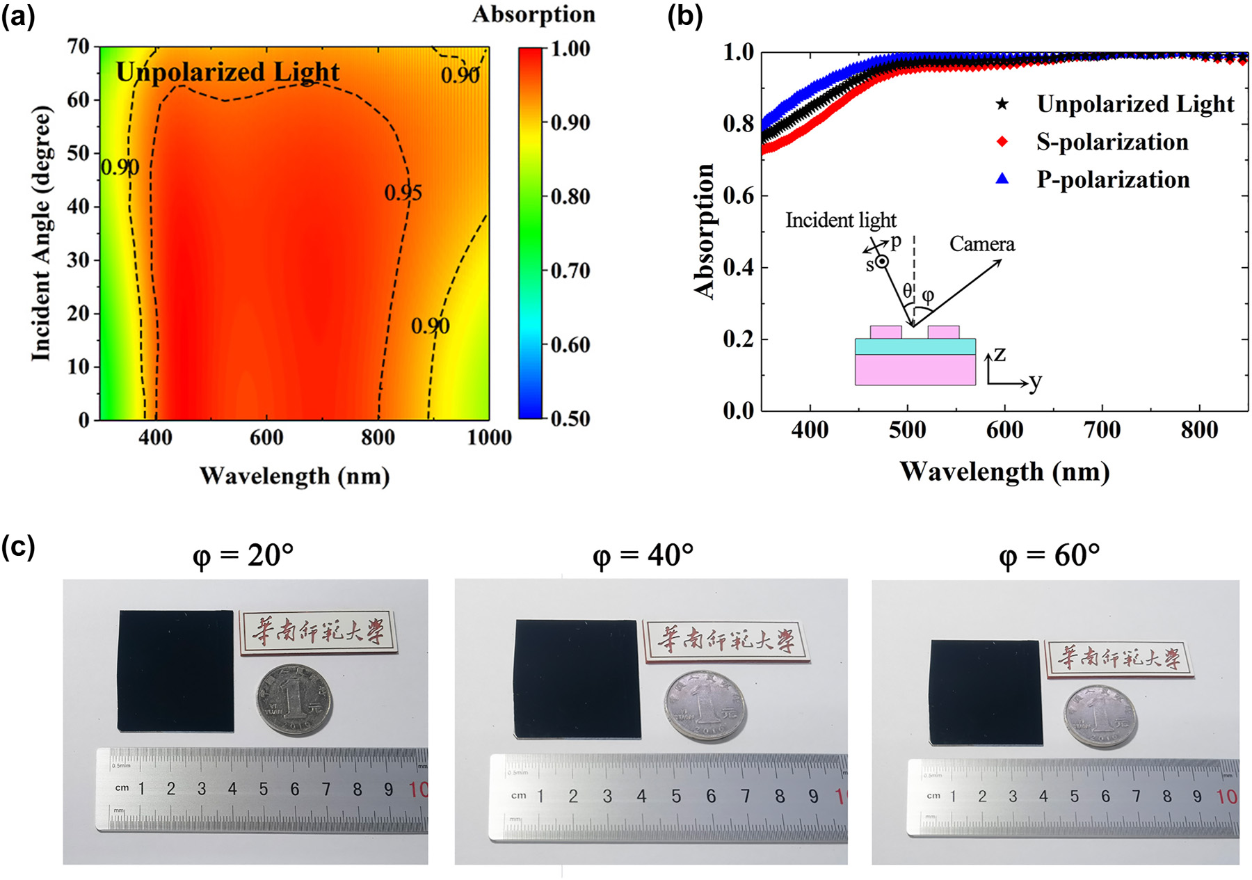
Omnidirectional absorption characterization. (a) Absorption spectrum versus incident angle for the metasurface absorber under unpolarized illumination. (b) Absorption spectra of the metasurface absorber at incident angle of 30° for s-polarized, p-polarized, and unpolarized light. (c) Digital camera images of the absorber sample taken at angles of 20°, 40°, 60°.
Note that such a strong absorption occurs in a 148 nm-thick structure. Average absorption in the entire visible region and structure thickness are two key performance metrics for absorbers applied to high-contrast and low-noise imaging. In Table 1, we list the key performance indicators of the state-of-the-art broadband absorbers working at visible wavelengths. It is seen that our device attains a record-high value of average-absorption/structure-thickness ratio among these broadband absorbers in the visible spectrum.
Comparison of the state-of-the-art broadband absorbers working in the visible region.
| Average absorption | Structure | Average absorption/ | Fabrication methods | Scalable | |
|---|---|---|---|---|---|
| in the entire visible | thickness | structure | manufacture | ||
| spectrum | (nm) | thickness (nm−1) | |||
| Li [5] | 0.91 | ∼2000 | <4.6 × 10⁻⁴ | Cu2+ ion etching, two-step Boehmite treatment, dip-coating | Yes |
| Kiani [6] | 0.99 | ∼30,000 | <3.3 × 10⁻⁵ | Thermal oxidation growth, hydrogen thermal reduction, self-catalytic chemical vapor deposition | Yes |
| Kim [8] | 0.91 | 40,040 | 2.3 × 10⁻⁵ | Capillary forced lithography, high step-coverage deposition, dry etching | Yes |
| Jia [10] | 0.96 | 240 | 4.0 × 10⁻³ | Magnetron sputtering, electron beam evaporation, electron beam lithography, dry etching | No |
| Chaudhuri [14] | 0.90 | 490 | 1.8 × 10⁻³ | Electron beam evaporation, electron beam lithography, dry etching | No |
| Qin [16] | 0.94 | 650 | 1.4 × 10⁻³ | Magnetron sputtering, ion beam sputtering, lithography, electron beam evaporation | No |
| Zhou [18] | 0.99 | 1085 | 9.1 × 10⁻⁴ | Two-step anodization method, template-assisted physical vapor deposition | Yes |
| Lee [21] | 0.95 | 268 | 3.5 × 10⁻³ | Colloidal self-assembly, reactive ion etching, electron beam evaporation | Yes |
| Hou [23] | 0.98 | 685 | 1.4 × 10⁻³ | Colloidal self-assembly, reactive ion etching, magnetron sputtering | Yes |
| Søndergaard [26] | 0.96 | 500 | 1.9 × 10⁻³ | Magnetron sputtering, focused ion beam | No |
| Lin [27] | 0.95 | 1030 | 9.2 × 10⁻⁴ | Laser writing, self-assembly graphene oxide coating, photo-induced reduction | No |
| Our work | 0.97 | 148 | 6.6 × 10⁻³ | Colloidal self-assembly, oxygen plasma etching, magnetron sputtering | Yes |
3 Discussion on absorption mechanism
We calculated the impedance of the considered metasurface using the S-parameter retrieval algorithm [28, 29]:
where μ
eff and ɛ
eff are the effective permeability and permittivity, respectively. The results are shown in Figure 5(a). It is seen that
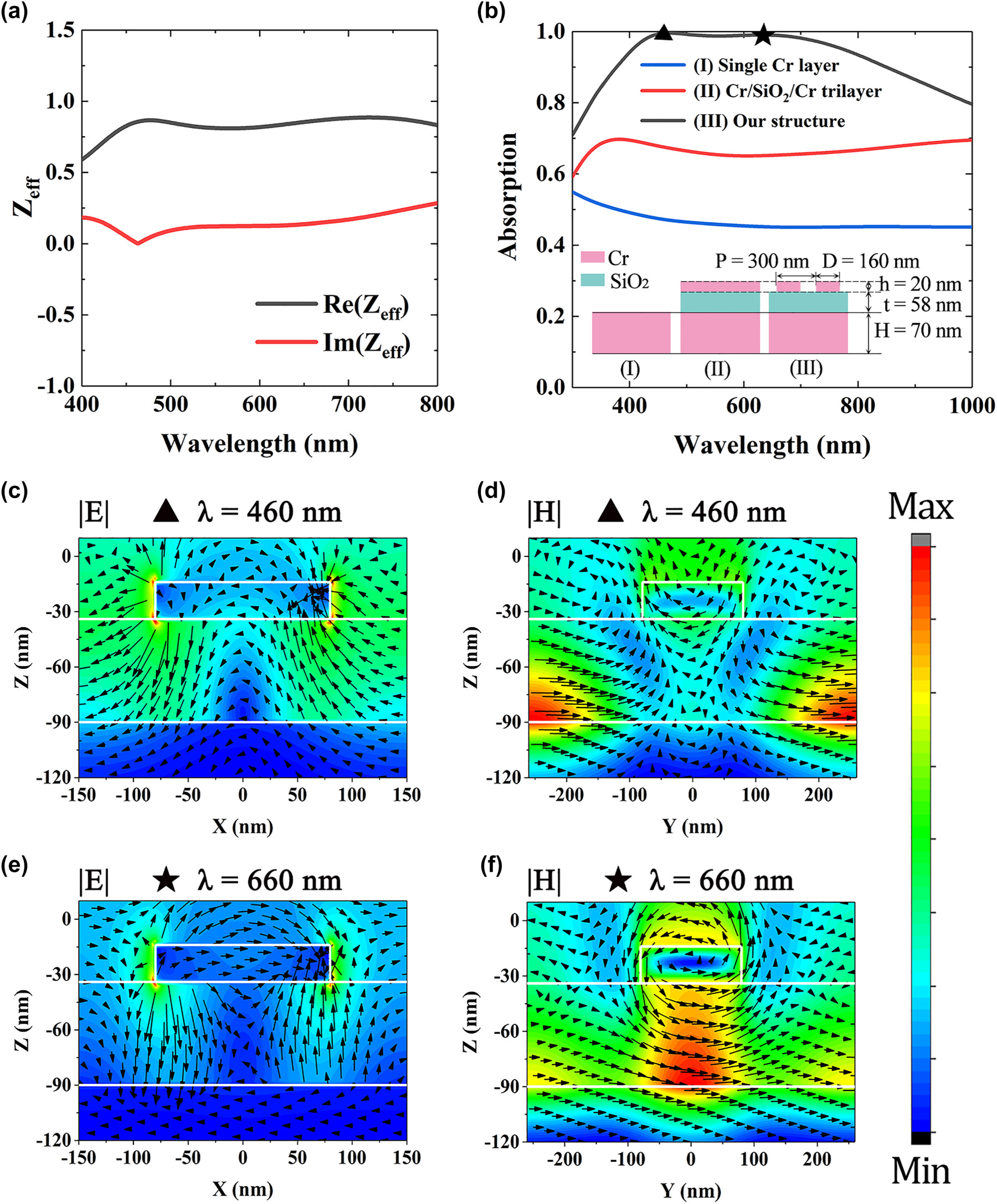
Illustration of absorption mechanism. (a) Impedance of the metasurface absorber. (b) Simulated absorption curves of bare Cr, Cr/SiO2/Cr trilayer, and our absorber. (c)–(f) Distributions of the electric field (E) (color maps) and the electric vectors (arrow maps) of the structure in x–z plane at (a) 460 nm and (c) 660 nm. Distributions of the magnetic field (H) and the magnetic vectors of the structure in y–z plane at (b) 460 nm and (d) 660 nm.
To reveal the physical mechanism of the broadband absorption, we show the absorption spectra of a single Cr thick layer, a Cr/SiO2/Cr trilayer, and our metasurface in Figure 5(b). It is seen that wideband absorption exists for the Cr thick layer because of its relatively large extinction coefficient. However, the absorption does not exceed 0.5 in the visible region. For the Cr/SiO2/Cr trilayer, the top and bottom Cr layers can be regarded as two opposite mirrors and they construct a resonant cavity. When light is vertically incident, Fabry–Perot (FP) resonance can be excited in the trilayer structure, resulting in the enhancement of absorption as shown in Figure 5(b). When the top Cr layer is replaced by the Cr nanodisk array, the absorption further increase because of the surface plasmon resonances. It is also seen that the absorption of the metasurface absorber reaches maxima at around 460 and 660 nm, respectively.
We then simulated the electric and magnetic field distributions in our absorber at wavelengths of 460 and 660 nm, as shown in Figure 5(c)–(f). It is seen from Figure 5(c) and (d) that the electric field is mainly localized at near both ends of the Cr nanodisk, while the magnetic field is localized in the gaps between the nanodisks. These field patterns agree with those of propagating surface plasmon (PSP), indicating the absorption peak around 460 nm is mainly contributed by the PSP resonance. Figure 5(e) and (f) show the electric and magnetic field distributions at wavelength of 660 nm. It is observed that strong field localization exists near the lower-ends of the Cr nanodisk and the magnetic vectors form a loop around the Cr nanodisk, indicating that an electric dipole exists (see Supplementary data 1 for details), which is consistent with the field local characteristics of localized surface plasmon (LSP) resonance. In addition, anti-parallel current forms inside the SiO2 layer and the magnetic field is strongly confined in the region below the Cr nanodisk, which is the symbol of the magnetic polariton (MP) resonance [22, 30, 31]. In this case, our metasurface structure can be equivalent to an LC circuit model and each unit cell can be regarded as a magnetic dipole (see Figure S2). When the total impedance of the LC model is zero, MP resonance can significantly enhance the absorption.
We also investigate the influence of the structural parameters on the performance of our metasurface absorber, as shown in Figure 6. Figure 6(a) and (b) show the simulated absorption spectra of the proposed metasurface absorber under different thickness t and materials of the dielectric spacer. As shown in Figure 6(a) and (b), with the increase of the thickness t or refractive index n of the dielectric spacer, a red shift of the absorption band can be observed. As the FP resonance exists between the top Cr nanodisks and the bottom Cr substrate, the increase of t or n leads to the increase of the optical path in the dielectric layer, thereby resulting in the red shift of the absorption band. Figure 6(c) and (d) show the absorption spectra of the proposed metasurface absorber under different height h and diameter D of the Cr nanodisks. It can be seen that as h or D increases, the position of the absorption peak at shorter wavelength remains almost unchanged, while the absorption peak at longer wavelength exhibits an obvious red shift. The reason for these phenomena is that the resonance wavelength of MP resonance increases with the increase of h or D (see Appendix A for details). Consequently, the broadband near-perfect absorption in our device is induced from FP, PSP, LSP and MP resonances.
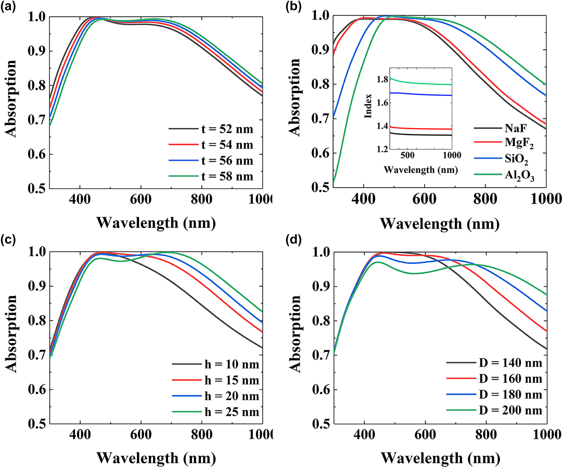
The absorption spectra of the metasurface absorber at different (a) t, (b) dielectric material, (c) h, (d) D. The other structural parameters are the same as those in Figure 1.
4 Conclusions
In summary, we reported a large area, ultrathin broadband visible light metasurface absorber composed of periodic Cr nanodisk array, a SiO2 film spacer, and a Cr substrate. The broadband perfect absorption was attributed to the combined effect of the Fabry–Perot resonance, the propagating and localized surface plasmons. The 148 nm-thick metasurface absorber has an average absorption over 97% in the wavelength range from 400 to 800 nm, which makes it suitable for absorption-based applications such as high-contrast medical and biological imaging. Our metasurface absorber is fabricated by a cost-effective, scalable, high-throughput self-assembly based process that does not require any lithography. With the development in the design and fabrication of different masks and templates, we expect that the self-assembly based nanofabrication technique will open up new scalable processing schemes for the large-scale manufacture of complex nanostructures, which could lead toward a diverse set of other applications, such as plasmonic lasers [32], nonlinear nanophotonic devices [33, 34], nanodevices with ultra-high Q [35], compact high-resolution color displays [36], etc.
Funding source: National Natural Science Foundation of China
Award Identifier / Grant number: 62035016
Funding source: Guangdong Provincial Key Laboratory
Award Identifier / Grant number: 2020B1212060066
Funding source: Guangdong Natural Science Foundation
Award Identifier / Grant number: 2015A030311018
Award Identifier / Grant number: 2017A030313035
Funding source: Science and Technology Program of Guangzhou
Award Identifier / Grant number: 2019050001
Funding source: Graduate Education Innovation Program
Award Identifier / Grant number: KA210314629
Funding source: Teaching Quality and Teaching Reform project
Award Identifier / Grant number: KA210314629
-
Author contribution: All the authors have accepted responsibility for the entire content of this submitted manuscript and approved submission.
-
Research funding: This work was funded by the National Natural Science Foundation of China (Grants No. 62035016), the Guangdong Natural Science Foundation (Grant Nos. 2015A030311018 and 2017A030313035), the Science and Technology Program of Guangzhou (Grant No. 2019050001), the Guangdong Provincial Key Laboratory (Grant No. 2020B1212060066), the Graduate Education Innovation Program (Grant No. KA200192325) and the Teaching Quality and Teaching Reform project (Grant No. KA210314629).
-
Conflict of interest statement: The authors declare no conflicts of interest regarding this article.
References
[1] Y. Cui, X. Wang, W. Ren, et al.., “Optical clearing delivers ultrasensitive hyperspectral dark-field imaging for single-cell evaluation,” ACS Nano, vol. 10, pp. 3132–3143, 2016. https://doi.org/10.1021/acsnano.6b00142.Search in Google Scholar PubMed PubMed Central
[2] Y. Kohmura, S. M. Yang, H. Chen, et al.., “The new X-ray/visible microscopy MAXWELL technique for fast three-dimensional nanoimaging with isotropic resolution,” Sci. Rep., vol. 12, p. 9668, 2022. https://doi.org/10.1038/s41598-022-13377-w.Search in Google Scholar PubMed PubMed Central
[3] F. Pfeiffer, M. Bech, O. Bunk, et al.., “Hard-X-ray dark-field imaging using a grating interferometer,” Nat. Mater., vol. 7, pp. 134–137, 2008. https://doi.org/10.1038/nmat2096.Search in Google Scholar PubMed
[4] H. Lin, B. C. P. Sturmberg, K. Lin, et al.., “A 90-nm-thick graphene metamaterial for strong and extremely broadband absorption of unpolarized light,” Nat. Photonics, vol. 13, pp. 270–276, 2019. https://doi.org/10.1038/s41566-019-0389-3.Search in Google Scholar
[5] Y. Li, Z. Huang, Y. Xu, et al.., “Scalable-manufactured ultrathin plasmonic metamaterial with omnidirectional absorption bandwidth across visible to far infrared,” Adv. Funct. Mater., vol. 14, p. 202207239, 2022. https://doi.org/10.1002/adfm.202207239.Search in Google Scholar
[6] F. Kiani, F. Sterl, T. V. Tsoulos, et al.., “Ultra-broadband and omnidirectional perfect absorber based on copper nanowire/carbon nanotube hierarchical structure,” ACS Photonics, vol. 7, no. 2, pp. 366–374, 2020. https://doi.org/10.1021/acsphotonics.9b01658.Search in Google Scholar
[7] M. Li, M. Shi, B. Wang, et al.., “Quasi-ordered nanoforests with hybrid plasmon resonances for broadband absorption and photodetection,” Adv. Funct. Mater., vol. 31, p. 2102840, 2021. https://doi.org/10.1002/adfm.202102840.Search in Google Scholar
[8] J. U. Kim, S. J. Kang, S. Lee, et al.., “Omnidirectional, broadband light absorption in a hierarchical nanoturf membrane for an advanced solar-vapor generator,” Adv. Funct. Mater., vol. 30, p. 2003862, 2020. https://doi.org/10.1002/adfm.202003862.Search in Google Scholar
[9] K. Bae, G. Kang, S. K. Cho, et al.., “Flexible thin-film black gold membranes with ultrabroadband plasmonic nanofocusing for efficient solar vapour generation,” Nat. Commun., vol. 6, p. 10103, 2015. https://doi.org/10.1038/ncomms10103.Search in Google Scholar PubMed PubMed Central
[10] H. Jia, C. Jiang, Q. Wu, et al.., “Broadband optical absorber based on nanopatterned metallic glass thin films,” J. Phys. Chem. Lett., vol. 10, no. 20, pp. 6055–6060, 2019. https://doi.org/10.1021/acs.jpclett.9b02526.Search in Google Scholar PubMed
[11] K. Aydin, V. E. Ferry, R. M. Briggs, et al.., “Broadband polarization-independent resonant light absorption using ultrathin plasmonic super absorbers,” Nat. Commun., vol. 2, p. 517, 2011. https://doi.org/10.1038/ncomms1528.Search in Google Scholar PubMed
[12] S. Sun, K. Yang, C. Wang, et al.., “High-Efficiency broadband anomalous reflection by gradient meta-surfaces,” Nano Lett., vol. 12, no. 12, pp. 6223–6229, 2012. https://doi.org/10.1021/nl3032668.Search in Google Scholar PubMed
[13] J. R. Hendrickson, S. Vangala, C. Dass, et al.., “Coupling of epsilon-near-zero mode to gap plasmon mode for flat-top wideband perfect light absorption,” ACS Photonics, vol. 5, no. 3, pp. 776–781, 2018. https://doi.org/10.1021/acsphotonics.7b01491.Search in Google Scholar
[14] K. Chaudhuri, M. Alhabeb, Z. Wang, et al.., “Highly broadband absorber using plasmonic titanium carbide (MXene),” ACS Photonics, vol. 5, no. 3, pp. 1115–1122, 2018. https://doi.org/10.1021/acsphotonics.7b01439.Search in Google Scholar
[15] B. Liu, C. Tang, J. Chen, et al.., “Multiband and broadband absorption enhancement of monolayer graphene at optical frequencies from multiple magnetic dipole resonances in metamaterials,” Nanoscale Res. Lett., vol. 13, p. 153, 2018. https://doi.org/10.1186/s11671-018-2569-3.Search in Google Scholar PubMed PubMed Central
[16] F. Qin, X. Chen, Z. Yi, et al.., “Ultra-broadband and wide-angle perfect solar absorber based on TiN nanodisk and Ti thin film structure,” Sol. Energy Mater. Sol. Cells, vol. 211, p. 110535, 2020. https://doi.org/10.1016/j.solmat.2020.110535.Search in Google Scholar
[17] S. A. Jalil, B. Lai, M. ElKabbash, et al.., “Spectral absorption control of femtosecond laser-treated metals and application in solar-thermal devices,” Light Sci. Appl., vol. 9, p. 14, 2020. https://doi.org/10.1038/s41377-020-0242-y.Search in Google Scholar PubMed PubMed Central
[18] L. Zhou, Y. Tan, D. Ji, et al.., “Self-assembly of highly efficient, broadband plasmonic absorbers for solar steam generation,” Sci. Adv., vol. 2, p. e1501227, 2016. https://doi.org/10.1126/sciadv.1501227.Search in Google Scholar PubMed PubMed Central
[19] W. Ali, M. F. Mideksa, K. Hou, et al.., “All-solution-processed ultrahigh broadband and wide-angle perfect absorber based on mxene–gold nanoparticles,” Adv. Opt. Mater., vol. 8, p. 2000447, 2020. https://doi.org/10.1002/adom.202000447.Search in Google Scholar
[20] H. Zhang, X. Feng, Y. Luo, et al.., “Colloidal self-assembly based all-metal metasurface absorbers to achieve broadband, polarization-independent light absorption at UV–Vis frequencies,” Appl. Surf. Sci., vol. 584, p. 152624, 2022. https://doi.org/10.1016/j.apsusc.2022.152624.Search in Google Scholar
[21] D. Lee, M. Go, M. Kim, et al.., “Multiple-patterning colloidal lithographyimplemented scalable manufacturing of heattolerant titanium nitride broadband absorbers in the visible to near-infrared,” Microsyst. Nanoeng., vol. 7, p. 14, 2021. https://doi.org/10.1038/s41378-020-00237-8.Search in Google Scholar PubMed PubMed Central
[22] H. Xu, L. Hu, Y. Lu, et al.., “Dual-band metamaterial absorbers in the visible and near-infrared regions,” J. Phys. Chem. C, vol. 123, pp. 10028–10033, 2019. https://doi.org/10.1021/acs.jpcc.9b00434.Search in Google Scholar
[23] W. Hou, F. Yang, Z. Chen, et al.., “Wide-angle and broadband solar absorber made using highly efficient large-area fabrication strategy,” Opt. Express, vol. 30, pp. 4424–4433, 2022. https://doi.org/10.1364/OE.451411.Search in Google Scholar PubMed
[24] W. Yu, Y. Lu, X. Chen, et al.., “Large-area, broadband, wide-angle plasmonic metasurface absorber for midwavelength infrared atmospheric transparency window,” Adv. Opt. Mater., vol. 7, p. 1900841, 2019. https://doi.org/10.1002/adom.201900841.Search in Google Scholar
[25] H. Xu, W. Rao, J. Meng, et al.., “Inverted hemispherical mask colloidal lithography,” Nanotechnology, vol. 20, p. 465608, 2009. https://doi.org/10.1088/0957-4484/20/46/465608.Search in Google Scholar PubMed
[26] T. Søndergaard, S. Novikov, T. Holmgaard, et al.., “Plasmonic black gold by adiabatic nanofocusing and absorption of light in ultra-sharp convex grooves,” Nat. Commun., vol. 3, p. 969, 2012. https://doi.org/10.1038/ncomms1976.Search in Google Scholar PubMed
[27] K. Lin, H. Lin, T. Yang, et al.., “Structured graphene metamaterial selective absorbers for high efficiency and omnidirectional solar thermal energy conversion,” Nat. Commun., vol. 11, p. 1389, 2020. https://doi.org/10.1038/s41467-020-15116-z.Search in Google Scholar PubMed PubMed Central
[28] D. R. Smith, S. Schultz, P. Marko, et al.., “Determination of effective permittivity and permeability of metamaterials from reflection and transmission coefficients,” Phys. Rev. B, vol. 65, p. 195104, 2002. https://doi.org/10.1103/PhysRevB.65.195104.Search in Google Scholar
[29] F. Ding, J. Dai, Y. Chen, et al.., “Broadband near-infrared metamaterial absorbers utilizing highly lossy metals,” Sci. Rep., vol. 6, p. 39445, 2016. https://doi.org/10.1038/srep39445.Search in Google Scholar PubMed PubMed Central
[30] P. Ekkels, X. Rottenberg, R. Puers, et al.., “Evaluation of platinum as a structural thin film material for RF-MEMS devices,” J. Micromech. Microeng., vol. 19, p. 065010, 2009. https://doi.org/10.1088/0960-1317/19/6/065010.Search in Google Scholar
[31] Y. Matsuno and A. Sakurai, “Perfect infrared absorber and emitter based on a large-area metasurface,” Opt. Mater. Express, vol. 7, pp. 618–626, 2017. https://doi.org/10.1364/OME.7.000618.Search in Google Scholar
[32] P. M. Oppeneer and V. Kapaklis, “Plasmonic lasers turn magnetic,” Nat. Photonics, vol. 16, pp. 11–13, 2022. https://doi.org/10.1038/s41566-021-00936-2.Search in Google Scholar
[33] M. Semmlinger, M. Tseng, J. Yang, et al.., “Vacuum ultraviolet light-generating metasurface,” Nano Lett., vol. 18, no. 9, pp. 5738–5743, 2018. https://doi.org/10.1021/acs.nanolett.8b02346.Search in Google Scholar PubMed
[34] K. Wang, A. Liu, H. Hsiao, et al.., “Large optical nonlinearity of dielectric nanocavity-assisted mie resonances strongly coupled to an epsilon-near-zero mode,” Nano Lett., vol. 22, no. 2, pp. 702–709, 2022. https://doi.org/10.1021/acs.nanolett.1c03876.Search in Google Scholar PubMed
[35] X. Xiao, Y. Lu, J. Jiang, et al.., “Manipulation of optical bound states in the continuum in a metal-dielectric hybrid nanostructure,” Photon. Res., vol. 10, pp. 2526–2531, 2022. https://doi.org/10.1364/PRJ.465119.Search in Google Scholar
[36] Z. Dong, J. Ho, Y. Yu, et al.., “Printing beyond sRGB color gamut by mimicking silicon nanostructures in free-space,” Nano Lett., vol. 17, no. 12, pp. 7620–7628, 2017. https://doi.org/10.1021/acs.nanolett.7b03613.Search in Google Scholar PubMed
Supplementary Material
This article contains supplementary material (https://doi.org/10.1515/nanoph-2022-0686).
© 2022 the author(s), published by De Gruyter, Berlin/Boston
This work is licensed under the Creative Commons Attribution 4.0 International License.
Articles in the same Issue
- Frontmatter
- Editorial
- Nanofabrication: the unsung hero in enabling advances in nanophotonics
- Reviews
- Semiconductor lasers with integrated metasurfaces for direct output beam modulation, enabled by innovative fabrication methods
- Deuterated SiNx: a low-loss, back-end CMOS-compatible platform for nonlinear integrated optics
- Research Articles
- Broadband spin-multiplexed single-celled metasurface holograms: a comprehensive comparison between different strategies
- Three-dimensionally reconfigurable focusing of laser by mechanically tunable metalens doublet with built-in holograms for alignment
- Reversible electrical switching of nanostructural color pixels
- Electrically switchable metallic polymer metasurface device with gel polymer electrolyte
- Telecom single-photon emitters in GaN operating at room temperature: embedment into bullseye antennas
- Gap solitons on an integrated CMOS chip
- Guided domino lithography for uniform fabrication of single-digit-nanometer scale plasmonic nanoantenna
- Nano-kirigami enabled chiral nano-cilia with enhanced circular dichroism at visible wavelengths
- Fabrication of quantum dot and ring arrays by direct laser interference patterning for nanophotonics
- Defining the zerogap: cracking along the photolithographically defined Au–Cu–Au lines with sub-nanometer precision
- Digital laser-induced printing of MoS2
- λ/20 surface nanostructuring of ZnO by mask-less ultrafast laser processing
- Circularly symmetric nanopores in 3D femtosecond laser nanolithography with burst control and the role of energy dose
- Multi-photon polymerization using upconversion nanoparticles for tunable feature-size printing
- 3D nanopolymerization and damage threshold dependence on laser wavelength and pulse duration
- Direct laser writing of 3D metallic mid- and far-infrared wave components
- Highly conformable terahertz metasurface absorbers via two-photon polymerization on polymeric ultra-thin films
- Photo-activated polymerization inhibition process in photoinitiator systems for high-throughput 3D nanoprinting
- Colloidal self-assembly based ultrathin metasurface for perfect absorption across the entire visible spectrum
- Enhanced electrochromic switching contrast in the blue by 3,4-propylenedioxypyrrole – implementation on structural colors
- Redeposition-free inductively-coupled plasma etching of lithium niobate for integrated photonics
- A universal metasurface transfer technique for heterogeneous integration