Highly conformable terahertz metasurface absorbers via two-photon polymerization on polymeric ultra-thin films
-
Andrea Ottomaniello

 ,
Paolo Vezio
,
Paolo Vezio

Abstract
The continuously increasing interest in flexible and integrated photonics requires new strategies for device manufacturing on arbitrary complex surfaces and with smallest possible size, respectively. Terahertz (THz) technology can particularly benefit from this achievement to make compact systems for emission, detection and on-demand manipulation of THz radiation. Here, we present a novel fabrication method to realize conformable terahertz metasurfaces. The flexible and versatile character of polymeric nanomembranes is combined with direct laser writing via two-photon polymerization to develop free-standing ultra-thin quasi-perfect plasmonic absorbers with an unprecedentedly high level of conformability. Moreover, revealing new flexible dielectric materials presenting low absorption and permittivity in the THz range, this work paves the way for the realization of ultra-thin, conformable hybrid or all-dielectric devices to enhance and enlarge the application of THz technologies, and flexible photonics in general.
1 Introduction
The full control of light propagation relies on the ability to engineer the interaction with matter at a subwavelength scale. In the general trend to consider systems of asymptotycally decreasing size, metasurfaces, the ultra-thin (quasi-2D) version of metamaterials, offer the most compact and efficient platform to achieve arbitrary manipulation of electromagnetic (EM) waves. Artificial micro- or nano- (metallo or/and dielectric) unit-structures can be arranged in a plane to obtain effective non-standard optical properties for ordinary matter, such as for example magnetism at optical frequencies [1], negative refractive index [2], zero reflection via impedance matching [3], perfect absorption [4], polarization control [5] or wavefront shaping [6]. As applications, a large plethora of metasurface devices have been developed, such as flat lenses, anomalous reflection/refraction deflectors, vortex plates, holograms and invisibility cloaks, just to name a few [7, 8].
Interestingly, their intrinsic two-dimensional character does not only provide compactness for planar integration on complex devices, but it also donates a high degree of structural flexibility and conformability to develop functional artificial “coating” layers. This peculiar property allows to target applications requiring arbitrary complex and curved geometries: for example, to decouple the optical properties of an object from its physical shape [9], to design surface patterns for molecular sensing and cryptography [10, 11] to create conformable holographic displays [12] or more in general to develop free-form devices [13] in the framework of flexible optics and photonics [14]. This demand for flexible, stretchable, non-planar systems and multifunctional materials has been the main lever for the research on innovative fabrication methods in recent years. Conventional micro- and nano-fabrication techniques have thus been oriented towards the exploitation of flexible, thin and/or elastomeric substrates to confer mechanical robustness and versatility to the designed metasurfaces. Depending on the specific operating frequency range, various fabrication techniques have been developed, enabling to build micrometer or nanometer scale elements on non-planar targets [15].
Across the EM spectrum, the terahertz (THz) frequency regime, spanning the range from 0.1 to 10 THz, significantly benefits from mechanically flexible metasurfaces which enhance the potential application of THz technology in fundamental physics studies, imaging, communication and sensing applications [16]. In this regard, a number of flexible devices have already been fabricated, for example to realize wide angle absorbers [17, 18], broadband quarter-wave plates [19] and different sensing applications [20, 21]. All these examples are united by the use of polymer matrices for the metasurface substrate, which offer versatile, large-area and low-cost fabrication. The most used ones are PDMS and polyimide, for their widespread use in flexible electronics, but also parylene, COC, BCB and PMMA and others can be found [22]. Their common characteristics are the low rigidity (low Young’s modulus), low absorption coefficient and low permittivity, which ensure high flexibility, low optical losses and large operating bandwidth, respectively. Onto these polymeric substrates, the resonator patterns are realized with well-established techniques, like conventional photolithography [23, 24] or shadow mask deposition [25], but also other methods such as soft lithography [26], transfer printing [27] and direct laser writing [28] have been demonstrated effective. However, each of these suffers from one or more drawbacks, which mostly limit them to at least several micrometers of thickness, and cause difficulty in transfer feasibility or/and moderate levels of conformability.
In this work, a novel fabrication method for ultra-sub-wavelength free-standing plasmonic metasurface THz absorbers with high degree of conformability is presented. The developed technique merges direct laser writing via two-photon polymerization (2PP) and transfer printing using ultra-thin polymeric membranes. In the 2PP nanolithography technique, femtosecond pulses of a standardly used near-infrared laser are focused inside photosensitive resins able to initiate polymerization at the laser beam spot. Only at this specific volume (called “voxel”) the laser intensity may be high enough to make two-photon absorption events possible triggering the polymer crosslinking, while elsewhere the photoresin is transparent to single photons. By moving the “voxel” inside the material using controlled highly accurate positioning systems, complex full three-dimensional (3D) micro-architectures can be printed in a single step. The threshold non-linear nature of the 2PP process allows beyond diffraction limit resolution of up to 100 nm or better [29]. Thanks to the 3D geometric flexibility and increasing availability of functionalized photoresins, direct laser writing by 2PP has enormous potential for the development of micro- and nano-metamaterials [30]. Here, while the 2PP process is performed to realize the metasurface geometry – the in-plane meta-molecules arrangements and the corresponding thickness – the enhanced spontaneous delamination of a few nanometers thin polyvinyl-formal layer (PVF) via substrate functionalization allows detaching and handling the entire structure after previous metallization. The whole device can be thus straightforwardly suspended or transferred onto a final target using different techniques, which are already demonstrated to allow delamination, suspension and transfer of three-dimensional 2PP structures onto unconventional non-planar surfaces [31]. The optical characterization performed by time-domain spectroscopy reveals that the used polymeric materials, PVF and the specific 2PP photoresin, present low absorption coefficient and permittivity at THz frequencies, thus making them ideal for THz light manipulation. Through a single deposition of a gold layer, two complementary metal patterns displaced by the thickness of the 2PP printed metasurface are created. This two-plane metal resonator distribution allows obtaining high plasmonic absorption resonances. Creating a double metal structure, by coupling a second metallized PVF film via Van der Waals adhesion to the bottom of the same, the optical absorption is strongly enhanced to get quasi-perfect levels in free-standing devices with out-of-plane dimension only a few % of the resonating wavelength. Owing to the ultra-thin thickness and high elasticity of the polymeric materials, objects with radius of curvature as low as tens of micrometers can be easily wrapped with the fabricated metasurfaces. The developed technique thus enlarges the current capabilities of fabricating flexible metamaterials with unprecedented performance in terms of conformability, extending their application in integrated and flexible optics and photonics.
2 Fabrication technique
The potential of ultra-thin (thickness less
Here, we exploit the same DM structure, but including an intermediate dielectric transparent material between the two metallizations which inscribes the metasurface pattern needed for generating the optical absorption resonance in the system. The fabrication procedure is schematized in Figure 1, and it can be summarized in six steps: (1) polymer layer spin-coating, (2) 2PP printing, (3) top metal deposition, (4) delamination, (5) collection and (6) bottom metallization. Two polished silicon wafers are processed in parallel and used as very low roughness substrates to obtain a perfectly homogeneous polymeric thin layer. Exploiting the technique described in [43], a 50 nm-thick PVF layer is created by spin-coating on both wafers after a previous sub-nm functionalization of the surface with a specific cationic electrolyte, which enables the polymeric film to spontaneously delaminate in water. On one of the two coated wafers a 2PP print is performed using a commercial photoresin (IP-Dip, from Nanoscribe) to realize the cross-linked polymeric matrix constituting the designed metasurface structure.
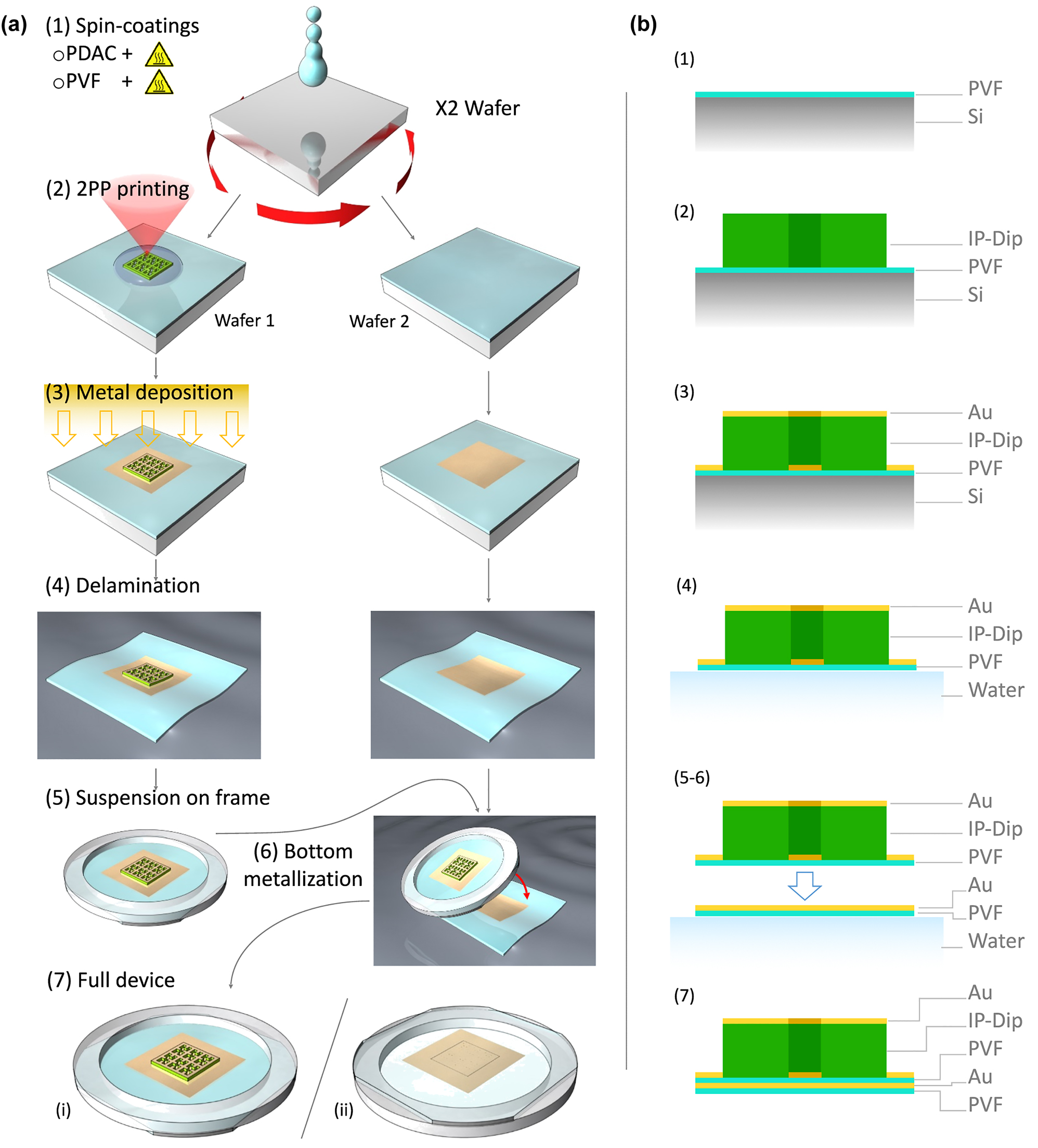
Fabrication process flow. (a) Steps of the fabrication of the ultra-thin conformable metasurface absorbers. (1) Spin-coating of the polymeric thin film on a silicon wafer. Two different wafers are processed in parallel. (2) Printing by 2PP of the IP-Dip cross-linked structure which acts both as dielectric spacer and pattern for the metallization of the device on the first wafer (left sample). (3) Shadow-mask deposition of a 50 nm-thick gold pad on both PVF coated silicon wafers over an area larger than the printed structure. (4) Delamination in water of the polymeric thin film of both wafers carrying the metallized metasurface and the gold pad (left and right samples, respectively). (5) Collection on a holed frame of the delaminated PVF film carrying the metallized 2PP structure. (6) Collection on the same frame of the second PVF film presenting the gold pad which is aligned to that of the metasurface in order to create its bottom metallization. (7) Top (i) and bottom (ii) view of the final device are shown by the left and right sketches, respectively. (b) Schematic profile of the metasurface unit-cell through the entire fabrication process.
This layer determines both the in-plane geometry of the metasurface and the thickness (from a few 100s nm up to several micrometers) of the dielectric layer of the final absorbers. The device top metallization is then realized by a shadow mask sputtering deposition of a 3 × 3 mm2-large 50 nm-thick gold pad which is aligned on top of the 2PP printed metasurface. Covering both the printed and unprinted regions of the metasurface design, two complementary metal patterns displaced by the cross-linked IP-Dip thickness are simultaneously realized by the sputtering deposition (as it will be highlighted in the following section). The same metallization process is also performed for the second PVF spin-coated silicon wafer. The whole device, now comprising the PVF layer plus the metalized 2PP metasurface, is still able to spontaneously delaminate in a water bath, and float on the water tension. The PVF film can thus be easily collected on a specific holed frame, to have the whole device freestanding on the ultra-thin polymeric layer. Finally, also the second PVF layer with the gold pad is delaminated and collected over the same holder. By aligning the metal pad with the metasurface structure, the bottom metallization is obtained and the entire DM metasurface absorbers completed. In the region where the 2PP print is present, the device at the end of the fabrication process is thus structured as follows starting from the bottom layer: PVF thin film, 50 nm-thick gold layer, PVF thin film, IP-dip dielectric with variable thickness and the top 50 nm-thick gold layer. Elsewhere, at the location of the unprinted parts where the development process has completely removed the not cross-linked IP-Dip, the device presents only the PVF plus the gold layers. A sketch of the final sample is shown in Figure 1a at point 7, where the top and back views are shown by the left and right illustration, respectively. In Figure 1b, the material composition of the device throughout the entire process is also reported. All details regarding the fabrication process are reported in the Supplementary Materials.
2.1 Device description
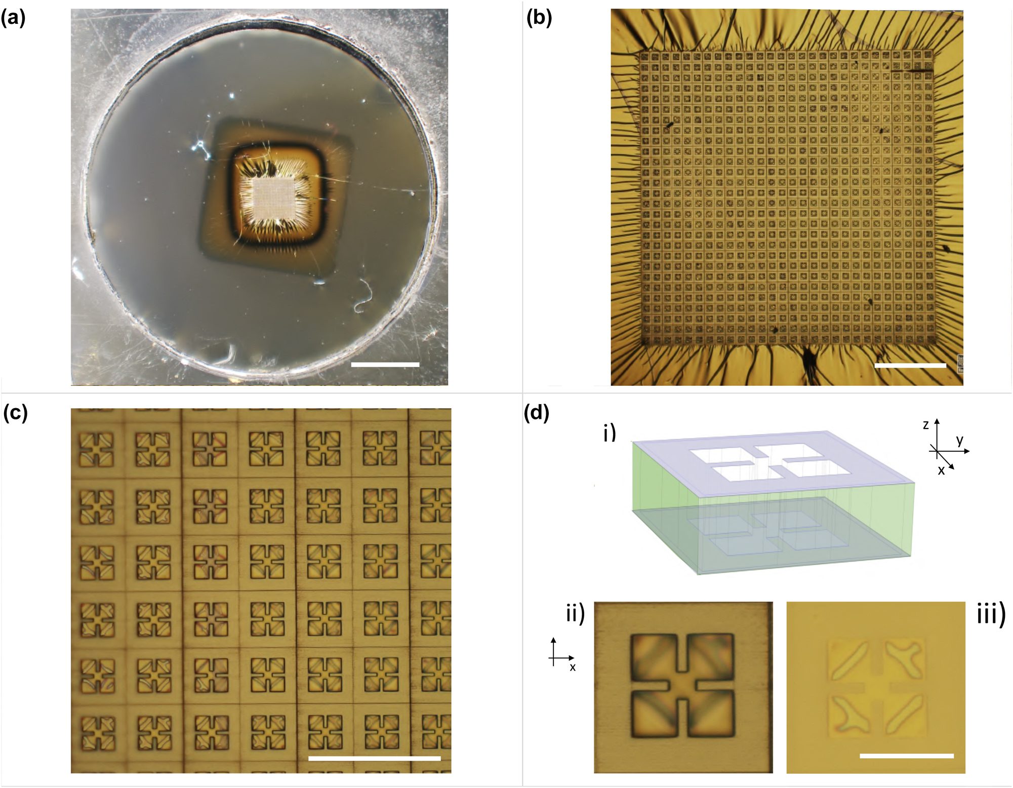
A fabricated sample presenting only the top metallization is shown in the optical image of Figure 2a. The circular holed frame with the flat suspended transparent PVF membrane can be recognized. At the center, the square 2 μm-thick metasurface absorber is distinguishable from the surrounding unpatterned metallization via a brighter gold color. Figure 2b and c show the metasurface pattern at increasing magnification where it is possible to observe the square array arrangement and geometry of the metasurface unit-cell with size a = 43 μm, respectively. The realized resonator shape belongs to the most widely used class of sub-wavelength optical resonators at microwave, THz and FIR frequencies known as split-ring resonators (SRRs), which can present electric and/or magnetic response by design [45]. SRRs-based metasurfaces have been demonstrated to be ideal to achieve also quasi-perfect absorption in DM structures. The working principle of these devices is the engineering of the whole EM response of the system. The dispersions of the effective electric permittivity and magnetic permeability can be independently controlled via the top metasurface design and its coupling with the underneath ground plane (where the induced currents generate the magnetic response), respectively. Interestingly, this can allow the EM impedance of the system to match that of the external medium at a particular resonant frequency or range of operation. This matching indeed ensures that all the power impinging on the metamaterial cannot be transmitted (due to the totally reflective ground plane) nor reflected, and thus it is almost totally absorbed by the system [46]. In this case, the resonator is electric SRRs, presenting LC resonance due to the presence of inductive and capacitive elements constituted by the two perpendicular metal gaps and the corresponding open loops created in the center of the top metallization, respectively. This is shown in Figure 2d (i) where the direct laser printed and unprinted parts of the resonator unit-cell (i.e. the external and internal part, respectively) are highlighted via a 3D sketch. Importantly, as the metal deposition covers both printed and unprinted surfaces, the metal deposition directly creates two aligned and complementary metal patterns in the system: one at the top of the cross-linked photoresin and one in the internal (not-printed) part displaced by the metasurface thickness, which directly lies on the supporting polymeric membrane. This can also be noted in Figure 2d (ii) and (iii), where the top and back view of the unit-cell is shown, respectively. From the top, the internal part of the resonator is observed to be out of focus, while the entire surface of the resonator is in focus from the back. This reveals the good flatness of the PVF freestanding layer carrying the metasurface after the whole fabrication process. The geometrical parameters of the SRR geometry are also reported in the same image. Their values are: p = 2 μm, g = 5.5 μm, w = 7 μm and a = 43 μm. Importantly, the metasurface unit-cell presents a C 4-symmetry which provides a polarization independent response at normal incidence.
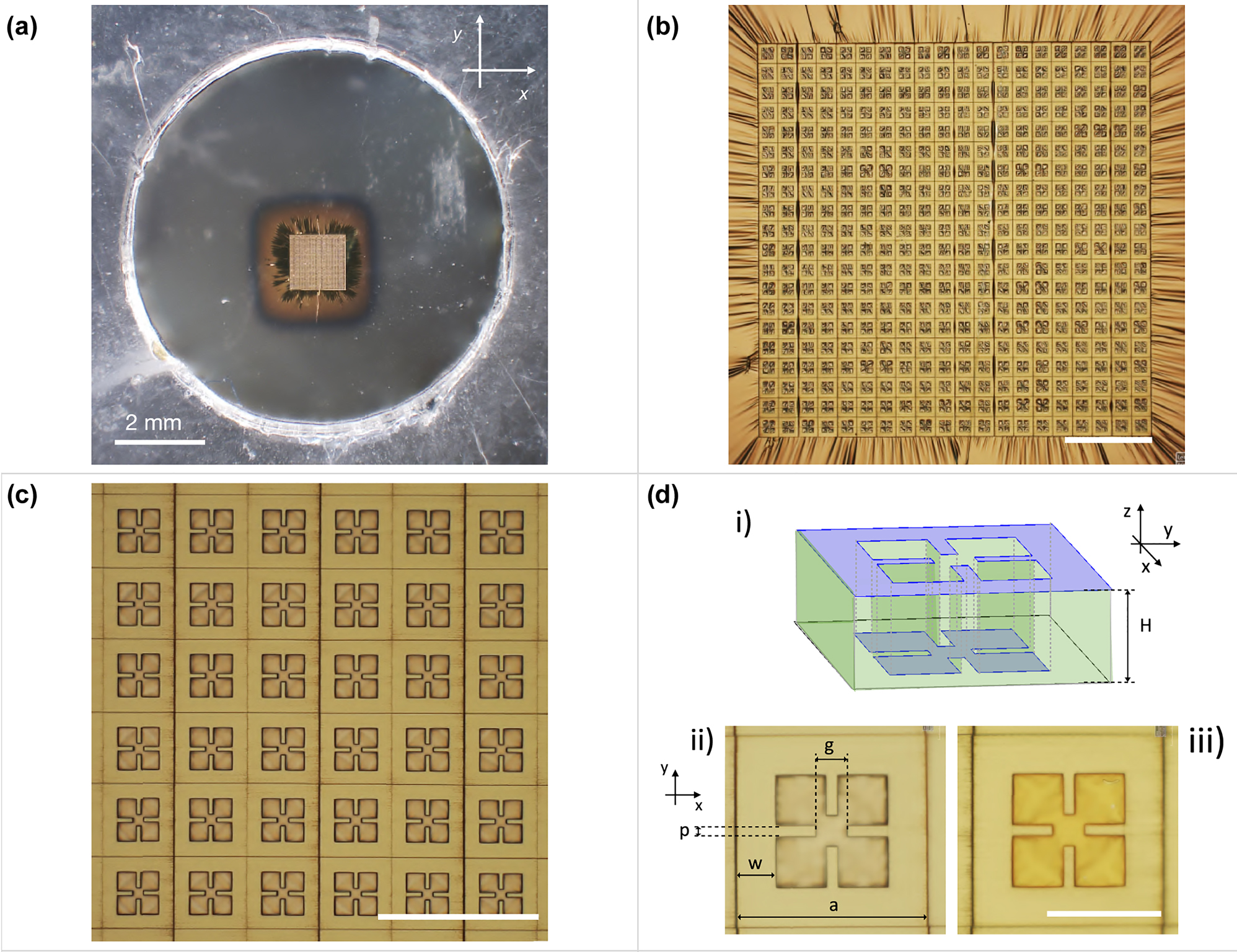
Optical images of a representative fabricated conformable THz metasurface absorber with only the top metallization. (a) Freestanding metasurface absorber on a 50 nm-thick PVF layer after delamination and collection on a holed frame. (b) 2PP patterned region of the ∼2 × 2 mm2-large, 2 μm-thick metasurface. (c) Zoom of the metasurface showing the square array of split ring resonators. (d) Scheme of the single metal metasurface unit-cell (i): 3D sketch highligthing (in violet color) the two complementary metal surfaces displaced by the resist thickness (green). The metasurface thickness was scaled by a factor 5 for clarity. Front (ii) and back (iii) view of the metasurface unit-cell of 45 μm-size. The resonator geometrical parameters are reported. Scale bars in (b), (c) and (d) are 200, 100 and 30 μm, respectively.
3 Optical characterization
In order to realize and design the metasurface absorbers at THz frequencies, the optical properties of the constituent materials were studied. In our case, the attention was focused on the two used polymers which are initially characterized in this frequency region: PVF and IP-Dip. The measurements were performed using time-domain spectroscopy (TDS) in the frequency range from 0.5 to 3.5 THz. The apparatus working in transmission configuration allowed to retrieve the refractive index n and absorption coefficient α from the amplitude change and phase shift of the transmitted signal with respect to the reference one. In Figure 3a, n and α dispersion of a suspended PVF thin film are shown. In order to obtain a measurable change with respect to the unperturbed reference signal, a 400 ± 5 nm-thick membrane was employed after spin-coating, delamination and collection on a holed frame. The refractive index is found to vary from 10 to 3 decreasing the frequency, while the absorption is low
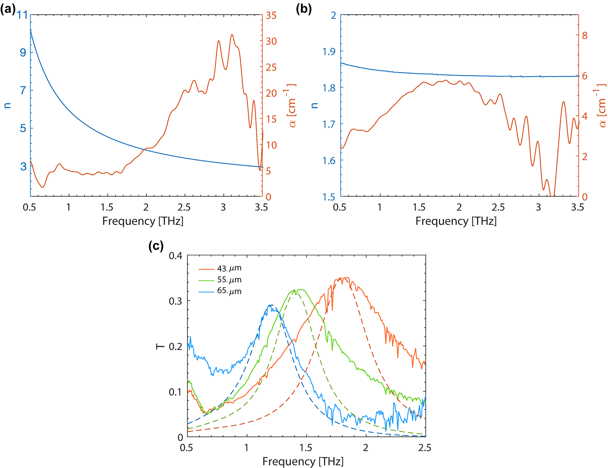
TDS characterization of PVF, IP-Dip and metasurface absorbers. Refractive index (n, blue curve) and absorption coeffcient (α, red curve) of PVF (a) and IP-Dip (b). (c) Transmission spectra for three metasurfaces having only the top metallization with 43, 55 and 65 μm unit-cell represented by the orange, green and blue solid curves, respectively. Dashed lines with same darker colors report the corresponding calculated results obtained via full-wave finite-element simulations.
Metasurfaces with different sizes of the unit-cell were realized exploiting the developed fabrication technique. Samples without the ground metal plane (processed until point 5 in Figure 1) were first characterized using the TDS set-up. The measurements were performed at atmospheric pressure in a dry air purged sample chamber to reduce its humidity concentration. A 2 mm diameter pin-hole is fixed in front of the sample in order to analyse only the transmitted signal from the metasurface region. A reference signal was measured with the same pin-hole aperture before the transmission measurements of each sample. The measured transmittance of three devices with a = 43 μm, 55 μm and 65 μm are shown in Figure 3c. The dielectric (IP-Dip) thickness of all samples is H = 2.5 μm, while the PVF film and the gold layer are 50 and 40 nm-thick, respectively. A low Q-factor
The comparison between the EM response of a SM metal metasurface and a DM device, i.e. presenting a 50 nm-thick ground plane metallization provided by the last fabrication step, is then investigated. The performed simulations of a SM and DM metasurface with a = 43 μm are shown in Figure 4a and b, respectively. These devices correspond to the samples shown in Figure 2 (SM device) and Figure 5 (DM device). The scattering matrices for light propagation are computed and reported as transmittance, reflectance and absorbance in the system. In agreement with the previously shown TDS measurements in Figure 2c (green curve), the SM device presents an absorption resonance around 1.8 THz with Q ∼ 3 and a peak absorbance of 28%. The in-plane EM field distribution (shown in Figure 4c (i)) at resonance can be observed to correspond to the excitation of the LC mode of the SRRs metasurface. The out-of-plane electric field E induced current density J in the top and bottom metallization patterns and Poynting vector P are also reported in Figure 4c (ii) and (iii), respectively. The relatively high absorption level can be explained by the built-in presence of two-complementary metal patterns (see Figure 4d) generating induced currents which are counter-circulating in the top and bottom gold layers displaced by the dielectric with thickness H = 2.5 μm. However, even if the coupling between the top and bottom metal patterns is able to produce an additional microcavity effect with high concentration of the EM field in the freestanding device (see Figure 4a (iii)), the incident power is largely reflected (37%) and transmitted (35%) by the system. Interestingly, when a ground metal plane is instead added to the system, the near-field distribution imposed by the coupling of the top metasurface with the uniform bottom metallization allows to achieve the targeted impedance matching between the system and the external medium (air) at a specific metasurface thickness (i.e. dielectric thickness). A quasi-perfect (99.5%) absorption peak with Q ∼ 12 emerges at 3.5 THz with a very low amount of reflected power
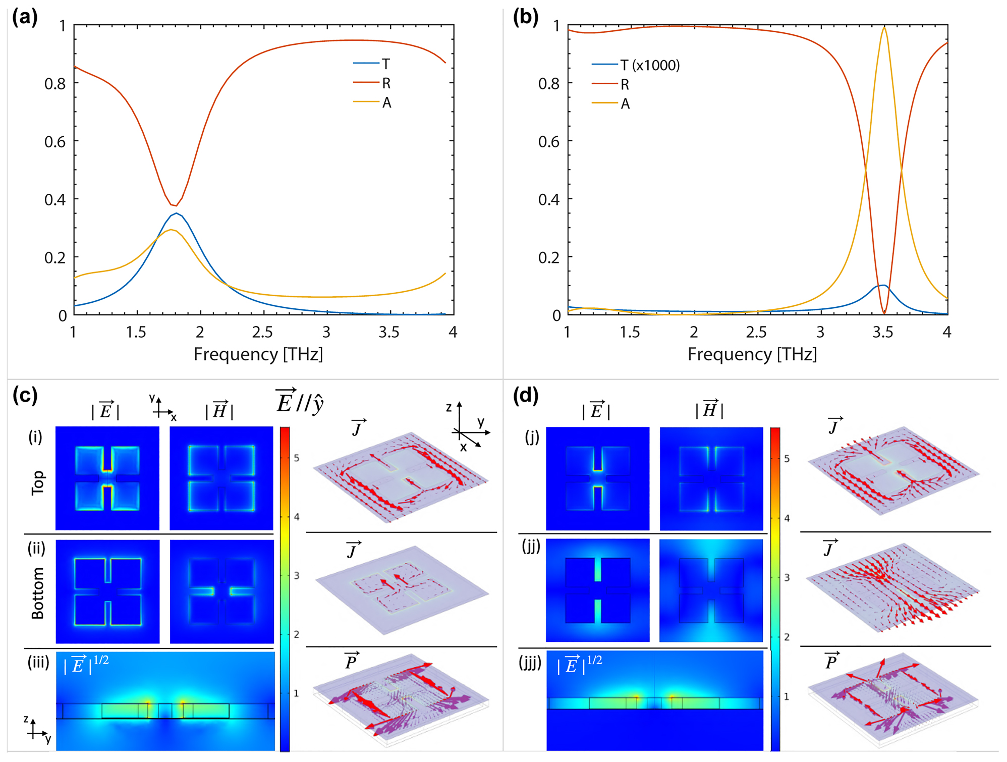
Simulated transmittance, reflectance and absorbance for a metasurface absorber with single (a) and double (b) metallization, with unit-cell size a = 43 μm. (c) Electric
Optical images of a conformable THz metasurface absorber where the top ground plane was added to form the DM-structure. (a) Freestanding DM absorber on the ultra-thin PVF layer at the end of the fabrication process. (b) Image of the 2 × 2 mm2 central region of the sample where the metasurface is located. (c) Zoom (700×) of the metasurface. (d) Scheme of the DM metal unit-cell (i): 3D sketch highlighting (in violet color) the top and bottom metal surfaces displaced by the resist thickness (green). The metasurface thickness was scaled by a factor 5 for clarity. Front (i) and (ii) back view of the metasurface unit-cell of 43 μm-size (×3000). Scale bars in (a), (b), (c) and (d) are 2000, 200, 100 and 30 μm, respectively.
The fabricated DM absorber with the same metasurface geometry and out-of-plane structure of the simulation to obtain the perfect-absorber at 3.5 THz is shown in Figure 5. In Figure 5a, the whole device suspended on the PVF layer can be seen. The larger square metallic pad having less bright gold color constitutes the underneath metal plane which is separated from the IP-Dip printed layer by two coupled 50 nm-thick PVF film. A very good and uniform adhesion between the first PVF layer carrying the metallized metasurface and the second one providing the bottom metal plane can be observed. This is highlighted also in Figure 5d (i) and (ii) where the top and bottom views of a single unit-cell are reported. Again the perfect Van der Waals adhesion ensures a very flat bottom surface guaranteeing agreement between the experimental and nominal distance of the top metasurface from the bottom ground plane.
In order to investigate the absorption in the fabricated devices, a single-mode quantum cascade laser (whose active region and operation details are reported in [47]) emitting at the metasurface resonance peak is used to measure the transmitted and reflected power from the freestanding SM and DM devices. The exploited apparatus is shown Figure 6a. A quantum cascade laser is powered in pulse mode at 10 kHz with 2%-duty cycle with an injected current of 1.4 A and kept at a temperature of 78 K by nitrogen liquid cooling to provide stable single-mode emission at
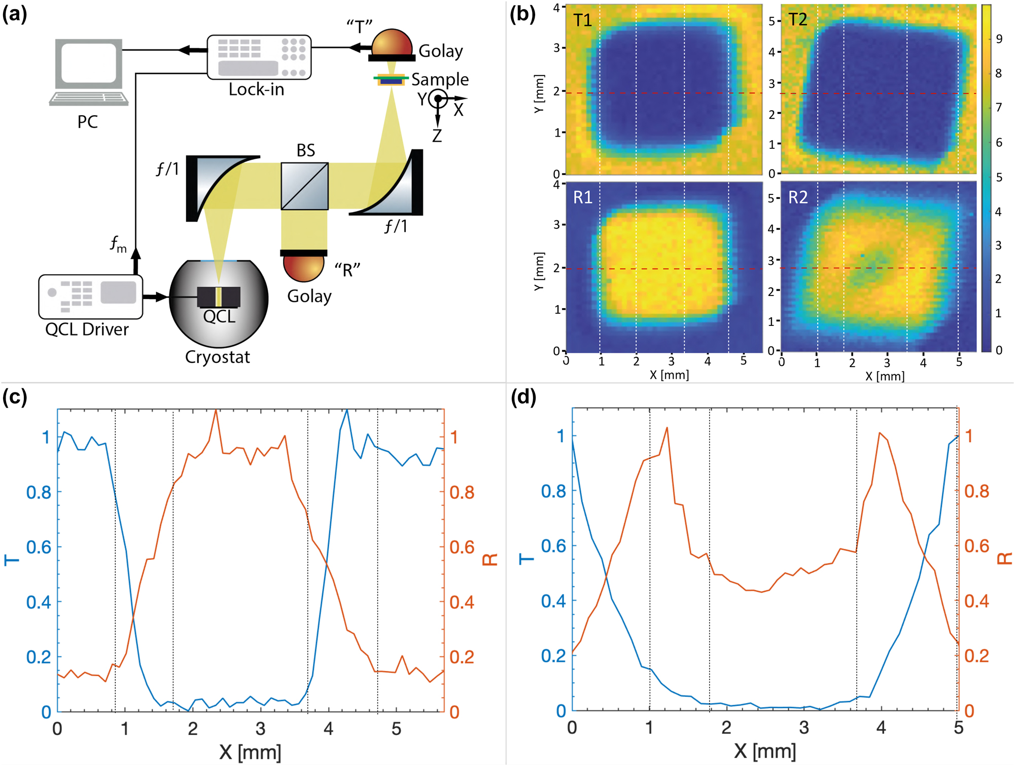
Imaging of the single and DM metasurfaces using a THz quantum cascade laser (QCL). (a) Scheme of the imaging apparatus. The emitted beam of a THz QCL (operating at 78 K and driven in pulse mode at 10 kHz with 2% duty cycle) is collimated and focused on the sample using two off-axis parabolic mirrors with 50 mm focal length. A Golay cell is used to detect the transmitted and reflected power from the sample by fixing it in position “T” and “R”, respectively. In reflection configuration, a beam splitter is fixed in between the two mirrors. The detected signal is electrically demodulated at ν m = 17 Hz using a lock-in amplifier. (b) Transmission (T) and reflection (R) images of a single metal (1) and a DM (2) metasurfaces with 43 μm unit-cell. (c) And (d) show the transmission and reflection profiles along the x-direction (reported in (b) as dashed red lines) for the single- and double-metal metasurfaces, respectively. Vertical dashed lines in (b) and (c) indicate the interface between different materials.
The degree of conformability of the developed metasurfaces was finally tested by transferring them on the cylindrical surface of metal wires. Metasurfaces with dimensions slightly larger than the circumference of the wire targeted for the transfer were thus fabricated. For the collection process on the wires we exploited the water transfer technique developed in [31]. This is performed by using a specific holder (reported in Figure 7a) where the metal wire is suspended in such a way to create a few millimeters high gap between the wire and the bottom surface of the holder. The PVF area enclosing the device to be delaminated is defined to have a side larger than twice this gap by applying a doctor blade to the spin-coated silicon wafer (as shown in the Supplementary Materials). After the delamination process of the PVF film, by immersing in water the holder carrying the suspended wire it is possible to collect the delaminated device floating on the water surface directly on top of the metal wire. During this process the water tension is able to create sufficient strain in the film through capillary forces to conform the metasurface to the wire cylindrical surface. The Van der Waals interaction of the polymer with the surface finally guarantees a very good and stable adhesion. Importantly, the defined gap is fundamental to avoid the PVF film to wrap multiple times on the wire surface during collection by the adhesion of film tails on the holder ground. The result of the water transfer of the film is shown in Figure 7a. At this point, the PVF ultra-thin layer in excess (i.e. not covered by the device metallization) can be easily removed by a standard descum process through oxygen-plasma etching (30 W for 60 s). Figure 7b and c show the perfect conformability of a SM device transferred on a 100 μm-diameter metal wire. The same transfer can be performed also for the DM device by performing two different transfers in series: one for the PVF carrying the bottom metallization and the second one to transfer the SM metasurface. Thanks to the ultra-thin fabricated metasurfaces and exploiting the developed water-based transfer technique, very low radii of curvature can be targeted. In our study, we in fact limited the conformability investigation to a curvature radius which was reasonable for the specific operating wavelength and corresponding resonator size.
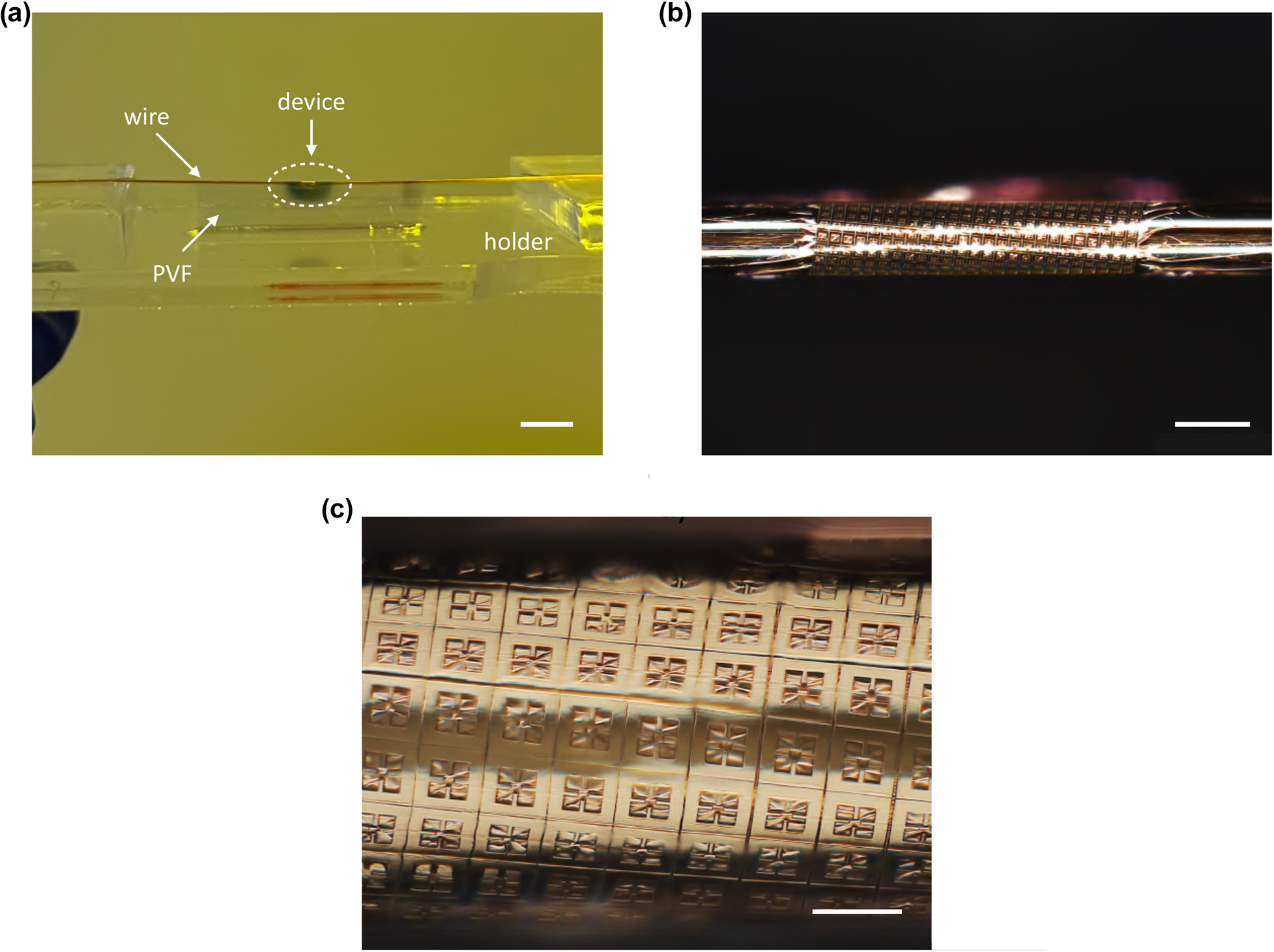
Demonstration of transfer on a high curvature target. (a) Optical image of the holder with the suspended copper wire wrapped by the THz metasurface aborber. (b) Image of the THz absorber showing the all-round conformability on the 100 μm-radius wire surface. (c) Zoom (700×) of the conformable device. Scale bars in (a), (b) and (c) are 5 mm, 250 μm and 50 μm, respectively.
Other demonstrations of high curvature conformability are obtained with metasurface absorbers with smallest unit-cell dimension (from 5 to 7 μm, resonating in the atmospheric window 23–37 THz) in order to be easily characterized in reflection by a Fourier-transform spectrometer equipped with an optical microscope to perform spectroscopy in a microscale range (see Supplementary Materials). On metasurfaces resonating around 25 THz, the absorption resonance frequency and amplitude are demonstrated to be not clearly affected by curvature indicating a limited dependence of the metasurface EM response at resonance from their curvature in the case of unpolarized incoming light. Moreover, the all-round transfer on cylindrical surfaces was successfully performed up (but not limited) to a minimum radius of curvature of 12.5 μm. This result demonstrates that, according to the specific operation frequency, the working flexibility of the developed conformable metasurfaces is only limited by the geometric metasurface design with respect to the curvature radius, optical properties of the materials, and, ultimately, by 2PP printing resolution.
4 Conclusions
A novel fabrication method for the realization of freestanding ultra-thin THz metasurfaces is described. The peculiarity of the technique is to merge the intrinsic ability of 2PP direct laser writing of creating dielectric structures with the flexibility of ultra-thin polymeric films to produce conformable plasmonic absorbers. Exploiting its spontaneous delamination in water, the polymeric nanomembrane can be in fact employed as freestanding support for the metallized 2PP printed metasurface structure. These devices were shown to present a relatively high level of absorption thanks to the built-in presence of two complementary metal planes arising in the structure after metallization. Upon creating a metal ground plane, achievable by coupling a second metal coated nanomembrane to the bottom of the structure, the devices can provide quasi-perfect resonant absorption. Importantly, owing to the ultra-thin thickness and high flexibility of the used polymeric material, the fabricated THz metasurface absorbers show unprecedented degree of conformability to high curvature surfaces. This is obtained through a water transfer process which allows all-round wrapping onto cylindrical surfaces with curvature as low as 12.5 μm in a straightforward and repeatable way. The proposed fabrication procedure can thus enable the realization of conformal metasurfaces for new lightweight, flexible or, eventually, wearable photonic devices. From a general perspective these devices can be suitable for integration in complex geometric systems, or they can be exploited for optical camouflage or information encryption in the emergent field of free-form optics. Strictly focusing on the THz frequency range, the extreme conformability combined with 3D geometrical flexibility of 2PP make them particularly beneficial for the realization of radar cross sectional reductors [48], and for the development of biosensors [49] in complex environments. Moreover, optical characterizations perfomed by TDS analysis show that the selected polymeric materials (PVF for the ultra-thin film and IP-Dip for the 2PP metasurface structure) have relatively low absorption losses and permittivity in the investigated range, revealing them as materials to be exploited at THz frequencies. Interestingly, the capacitor-like structure of the device created by the connected top metallization and bottom ground plane can be exploited in different ways: for example, to perform direct measurement of the capacitive dependence of the system upon illumination to form metasurface-based thermal detectors, or, it can also serve as gate to vary the EM response of the system to create dynamically tunable metasurfaces, provided that electric-field responsive material is integrated in the system.
In summary, owing to the presented novel fabrication method of freestanding highly conformable THz metasurfaces and for the new suitable materials introduced for this frequency range, this work can allow and ease the development of ultra-thin, flexible hybrid or all-dielectric THz devices which may boost the application of THz technology, and flexible photonics in general.
Funding source: European Union’s Horizon 2020
Award Identifier / Grant number: 899349
Funding source: Engineering and Physical Sciences Research Council Programme grant “HyperTerahertz”
Award Identifier / Grant number: EP/P021859/1
Acknowledgement
The authors gratefully thanks Edmund Linfield, Lianhe Li and Mohammed Salih for providing the quantum cascade laser exploited for the imaging measurement.
-
Author contributions: All the authors have accepted responsibility for the entire content of this submitted manuscript and approved submission.
-
Research funding: The authors gratefully acknowledge support from the European Union’s Horizon 2020 research and innovation program under the FET Open grant agreement 5DNanoPrinting – no. 899349. P.D. acknowledges support from the Engineering and Physical Sciences Research Council Programme grant “HyperTerahertz” (No. EP/P021859/1).
-
Conflict of interest statement: The authors declare no conflicts of interest regarding this article.
References
[1] S. Linden, C. Enkrich, G. Dolling, et al.., “Photonic metamaterials: magnetism at optical frequencies,” IEEE J. Sel. Top. Quantum Electron., vol. 12, no. 6, pp. 1097–1105, 2006. https://doi.org/10.1109/JSTQE.2006.880600.Search in Google Scholar
[2] V. Veselago, L. Braginsky, V. Shklover, and C. Hafner, “Negative refractive index materials,” J. Comput. Theor. Nanosci., vol. 3, no. 2, pp. 189–218, 2006. https://doi.org/10.1166/jctn.2006.3000.Search in Google Scholar
[3] T. C. Beh, M. Kato, T. Imura, S. Oh, and Y. Hori, “Automated impedance matching system for robust wireless power transfer via magnetic resonance coupling,” IEEE Trans. Ind. Electron., vol. 60, no. 90, p. 207402, 2012. https://doi.org/10.1109/TIE.2012.2206337.Search in Google Scholar
[4] N. I. Landy, S. Sajuyigbe, J. J. Mock, D. R. Smith, and W. J. Padilla, “Perfect metamaterial absorber,” Phys. Rev. Lett., vol. 100, no. 20, pp. 3689–3698, 2008. https://doi.org/10.1103/PhysRevLett.100.207402.Search in Google Scholar PubMed
[5] J. P. B. Mueller, N. A. Rubin, R. C. Devlin, B. Groever, and F. Capasso, “Metasurface polarization optics: independent phase control of arbitrary orthogonal states of polarization,” IEEE Trans. Ind. Electron., vol. 60, no. 90, p. 207402, 2012. https://doi.org/10.1103/PhysRevLett.118.113901.Search in Google Scholar PubMed
[6] B. Walther, C. Helgert, C. Rockstuhl, et al.., “Spatial and spectral light shaping with metamaterials,” Adv. Mater., vol. 24, no. 47, pp. 6300–6304, 2012. https://doi.org/10.1002/adma.201202540.Search in Google Scholar PubMed
[7] H. T. Chen, A. J. Taylor, and N. Yu, “A review of metasurfaces: physics and applications,” Rep. Prog. Phys., vol. 79, no. 7, p. 076401, 2016. https://doi.org/10.1088/0034-4885/79/7/076401.Search in Google Scholar PubMed
[8] N. Yu and F. Capasso, “Flat optics with designer metasurfaces,” Nat. Mater., vol. 12, no. 2, pp. 139–150, 2014. https://doi.org/10.1038/nmat3839.Search in Google Scholar PubMed
[9] S. M. Kamali, A. Arbabi, E. Arbabi, Y. Horie, and A. Faraon, “Decoupling optical function and geometrical form using conformal flexible dielectric metasurfaces,” Nat. Commun., vol. 7, no. 1, pp. 1–7, 2016. https://doi.org/10.1038/ncomms11618.Search in Google Scholar PubMed PubMed Central
[10] Y. Wang, C. Zhao, J. Wang, et al.., “Wearable plasmonic-metasurface sensor for noninvasive and universal molecular fingerprint detection on biointerfaces,” Sci. Adv., vol. 7, no. 4, p. eabe4553, 2021. https://doi.org/10.1126/sciadv.abe4553.Search in Google Scholar PubMed
[11] X. Liu, J. Wang, L. Tang, L. Xie, and Y. Ying, “Flexible plasmonic metasurfaces with user-designed patterns for molecular sensing and cryptography,” Adv. Funct. Mater., vol. 26, no. 30, pp. 5515–5523, 2016. https://doi.org/10.1002/adfm.201601154.Search in Google Scholar
[12] J. Burch and A. Di Falco, “Holography using curved metasurfaces,” Photonics, vol. 6, no. no. 1, p. 8, 2019. https://doi.org/10.3390/photonics6010008.Search in Google Scholar
[13] K. Wu, P. Coquet, Qi J. Wang, and P. Genevet, “Modelling of free-form conformal metasurfaces,” Nat. Commun., vol. 9, no. 1, pp. 1–8, 2018. https://doi.org/10.1038/s41467-018-05579-6.Search in Google Scholar PubMed PubMed Central
[14] G. C. Righini, J. Krzak, A. Lukowiak, G. Macrelli, S. Varas, and M. Ferrari, “From flexible electronics to flexible photonics: a brief overview,” Opt. Mater., vol. 115, p. 1111011, 2021. https://doi.org/10.1016/j.optmat.2021.111011.Search in Google Scholar
[15] S. Walia, C. M. Shah, P. Gutruf, et al.., “Flexible metasurfaces and metamaterials: a review of materials and fabrication processes at micro-and nano-scales,” Appl. Phys. Rev., vol. 2, no. 11, p. 011303, 2015. https://doi.org/10.1063/1.4913751.Search in Google Scholar
[16] S. S. Dhillon, M. S. Vitiello, E. H. Linfield, et al.., “The 2017 terahertz science and technology roadmap,” J. Phys. D: Appl. Phys., vol. 50, no. 4, p. 043001, 2017. https://doi.org/10.1088/1361-6463/50/4/043001.Search in Google Scholar
[17] H. Tao, C. M. Bingham, A. C. Strikwerda, et al.., “Highly flexible wide angle of incidence terahertz metamaterial absorber: design, fabrication, and characterization,” Phys. Rev. B, vol. 78, no. 24, p. 241103, 2008. https://doi.org/10.1103/PhysRevB.78.241103.Search in Google Scholar
[18] K. Fan, X. Zhao, J. Zhang, et al.., “Optically tunable terahertz metamaterials on highly flexible substrates,” IEEE Trans. Terahertz Sci. Technol., vol. 3, no. 6, pp. 702–708, 2013. https://doi.org/10.1109/TTHZ.2013.2285619.Search in Google Scholar
[19] L. Cong, N. Xu, J. Gu, R. Singh, J. Han, and W. Zhang, “Highly flexible broadband terahertz metamaterial quarter-wave plates,” Laser Photonics Rev., vol. 8, no. 4, pp. 626–632, 2014. https://doi.org/10.1002/lpor.201300205.Search in Google Scholar
[20] J. Li, C. M. Shah, W. Withayachumnankul, et al.., “Flexible terahertz metamaterials for dual-axis strain sensing,” Opt. Lett., vol. 38, no. 12, pp. 2104–2106, 2013. https://doi.org/10.1364/OL.38.002104.Search in Google Scholar PubMed
[21] X. Zhang, Y. Wang, Z. Cui, et al.., “Carbon nanotube-based flexible metamaterials for THz sensing,” Opt. Mater. Express, vol. 11, no. 5, pp. 1470–1483, 2021. https://doi.org/10.1364/OME.424693.Search in Google Scholar
[22] R. T. Ako, A. Upadhyay, W. Withayachumnankul, M. Bhaskaran, and S. Sriram, “Dielectrics for terahertz metasurfaces: material selection and fabrication techniques,” Adv. Opt. Mater., vol. 8, no. 3, p. 1900750, 2020. https://doi.org/10.1002/adom.201900750.Search in Google Scholar
[23] I. E. Khodasevych, C. M. Shah, S. Sriram, et al.., “Elastomeric silicone substrates for terahertz fishnet metamaterials,” Nat. Protoc., vol. 100, no. 6, p. 061101, 2012. https://doi.org/10.1063/1.3665180.Search in Google Scholar
[24] X. Liu, S. MacNaughton, D. B. Shrekenhamer, et al.., “Metamaterials on parylene thin film substrates: design, fabrication, and characterization at terahertz frequency,” Appl. Phys. Lett., vol. 96, no. 1, p. 011906, 2010. https://doi.org/10.1063/1.3275015.Search in Google Scholar
[25] S. Aksu, M. Huang, A. Artar, et al.., “Flexible plasmonics on unconventional and nonplanar substrates,” Adv. Mater., vol. 23, no. 38, pp. 4422–4430, 2011. https://doi.org/10.1002/adma.201102430.Search in Google Scholar PubMed
[26] D. Qin, Y. Xia, and G. M. Whitesides, “Soft lithography for micro-and nanoscale patterning,” Nat. Protoc., vol. 5, no. 3, p. 491, 2010. https://doi.org/10.1038/nprot.2009.234.Search in Google Scholar PubMed
[27] M. A. Meitl, Z. T. Zhu, V. Kumar, et al.., “Transfer printing by kinetic control of adhesion to an elastomeric stamp,” Nat. Mater., vol. 5, no. 1, pp. 33–38, 2006. https://doi.org/10.1038/nmat1532.Search in Google Scholar
[28] T. Bückmann, N. Stenger, M. Kadic, et al.., “Tailored 3D mechanical metamaterials made by dip-in direct-laser-writing optical lithography,” Adv. Mater., vol. 24, no. 20, pp. 2710–2714, 2012. https://doi.org/10.1002/adma.201200584.Search in Google Scholar PubMed
[29] G. Seniutinas, A. Weber, C. Padeste, I. Sakellari, M. Farsari, and C. David, “Beyond resolution 100 nm in 3D laser lithography – post processing solutions,” Microelectron. Eng., vol. 191, pp. 25–31, 2018. https://doi.org/10.1016/j.mee.2018.01.018.Search in Google Scholar
[30] V. Harinarayana and Y. C. Shin, “Two-photon lithography for three-dimensional fabrication in micro/nanoscale regime: a comprehensive review,” Opt. Laser Technol., vol. 142, p. 107180, 2021. https://doi.org/10.1016/j.optlastec.2021.107180.Search in Google Scholar
[31] F. Den Hoed, A. Ottomaniello, O. Tricinci, L. Cesarecciu, M. Carlotti, P. Raffa and V. Mattoli, “Facile handling of two-photon polymerized 3D microstructures by ultra-conformable freestanding polymeric membranes,” Adv. Funct. Mater., 2023, submitted for publication.10.1002/adfm.202214409Search in Google Scholar
[32] R. Vendamme, S. Y. Onoue, A. Nakao, and T. Kunitake, “Robust free-standing nanomembranes of organic/inorganic interpenetrating networks,” Nat. Mater., vol. 5, no. 6, pp. 494–501, 2006. https://doi.org/10.1038/nmat1655.Search in Google Scholar PubMed
[33] C. Jiang, S. Markutsya, Y. Pikus, and V. V. Tsukruk, “Freely suspended nanocomposite membranes as highly sensitive sensors,” Nat. Mater., vol. 3, no. 10, pp. 721–728, 2004. https://doi.org/10.1038/nmat1212.Search in Google Scholar PubMed
[34] T. Fujie, L. Ricotti, A. Desii, A. Menciassi, P. Dario, and V. Mattoli, “Evaluation of substrata effect on cell adhesion properties using freestanding polymeric nanosheets,” Langmuir, vol. 27, no. 21, pp. 13173–13182, 2011. https://doi.org/10.1021/la203140a.Search in Google Scholar PubMed
[35] A. D. Fujie, L. Ventrelli, B. Mazzolai, and V. Mattoli, “Inkjet printing of protein microarrays on freestanding polymeric nanofilms for spatio-selective cell culture environment,” Biomed. Microdevices, vol. 14, no. 21, pp. 1069–1076, 2012. https://doi.org/10.1007/s10544-012-9698-8.Search in Google Scholar PubMed
[36] E. Redolfi Riva, A. Desii, S. Sartini, C. La Motta, B. Mazzolai, and V. Mattoli, “PMMA/polysaccharides nanofilm loaded with adenosine deaminase inhibitor as a platform for targeted anti-inflammatory drug delivery,” Langmuir, vol. 29, no. 43, pp. 13190–13197, 2013. https://doi.org/10.1021/la402229k.Search in Google Scholar PubMed
[37] E. Ridolfi Riva, A. Desii, E. Sinibaldi, et al.., “Gold nanoshell/polysaccharides nanofilm for controlled laser-assisted tissue thermal ablation,” ACS Nano, vol. 8, no. 6, pp. 5552–5563, 2014. https://doi.org/10.1021/nn406348v.Search in Google Scholar PubMed
[38] S. Taccola, F. Greco, A. Zucca, et al.., “Characterization of free-standing PEDOT:PSS/iron oxide nanoparticles composite thin films and application as conformable humidity sensors,” ACS Appl. Mater. Interfaces, vol. 5, no. 13, pp. 6324–6332, 2013. https://doi.org/10.1021/am4013775.Search in Google Scholar PubMed
[39] S. Taccola, F. Greco, B. Mazzolai, V. Mattoli, and E. W. H. Jager, “Thin film free standing PEDOT:PSS/SU8 bilayer microactuators,” J. Micromech. Microeng., vol. 24, p. 465102, 2013. https://doi.org/10.1088/0960-1317/23/11/117004.Search in Google Scholar
[40] F. A. Viola, J. Barsotti, F. Melloni, et al.., “A sub 150 nanometers thick and ultra-conformable solution processed all-organic transistor,” Nat. Commun., vol. 12, p. 5842, 2021. https://doi.org/10.1038/s41467-021-26120-2.Search in Google Scholar PubMed PubMed Central
[41] F. Greco, A. Zucca, S. Taccola, B. Mazzolai, and V. Mattoli, “Patterned free-standing conductive nanofilms for ultra-conformable circuits and smart interfaces,” ACS Appl. Mater. Interfaces, vol. 5, no. 19, pp. 9461–9469, 2013. https://doi.org/10.1021/am402142c.Search in Google Scholar PubMed
[42] J. Barsotti, I. Hirata, F. Pignatelli, M. Caironi, F. Greco, and V. Mattoli, “Ultraconformable freestanding capacitors based on ultrathin polyvinyl formal films,” Adv. Electron. Mater., vol. 4, no. 11, p. 1800215, 2018. https://doi.org/10.1002/aelm.201800215.Search in Google Scholar
[43] S. H. Baxamusa, M. Stadermann, C. Aracne-Ruddle, et al.., “Enhanced delamination of ultrathin free-standing polymer films via self-limiting surface modification,” Langmuir, vol. 30, no. 18, pp. 5126–5132, 2014. https://doi.org/10.1021/la5011665.Search in Google Scholar PubMed
[44] C. M. Watts, X. Liu, and W. J. Padilla, “Metamaterial electromagnetic wave absorbers,” Adv. Mater., vol. 24, no. 23, pp. OP98–OP120, 2012. https://doi.org/10.1002/adma.201200674.Search in Google Scholar PubMed
[45] W. Withayachumnankul and D. Abbott, “Metamaterials in the terahertz regime,” IEEE Photonics J., vol. 1, no. 2, pp. 99–118, 2009. https://doi.org/10.1109/JPHOT.2009.2026288.Search in Google Scholar
[46] Hu Tao, N. I. Landy, C. M. Bingham, X. Zhang, R. D. Averitt, and W. J. Padilla, “A metamaterial absorber for the terahertz regime: design, fabrication and characterization,” Opt. Express, vol. 16, no. 10, pp. 7181–7188, 2008. https://doi.org/10.1364/OE.16.007181.Search in Google Scholar
[47] M. Wienold, L. Schrottke, M. Giehler, R. Hey, W. Anders, and H. T. Grahn, “Low-voltage terahertz quantum-cascade lasers based on LO-phonon-assisted interminiband transitions,” Electron. Lett., vol. 45, no. 20, pp. 1030–1031, 2009.10.1049/el.2009.1371Search in Google Scholar
[48] W. Yin, Z. Shen, S. Li, et al.., “Flexible broadband terahertz absorbers for RCS reduction on conformal surfaces,” Opt. Commun., vol. 520, p. 128502, 2022. https://doi.org/10.1016/j.optcom.2022.128502.Search in Google Scholar
[49] W. Yin, Z. Shen, Y. Cui, et al.., “Highly sensitive terahertz sensing with 3D-printed metasurfaces empowered by a toroidal dipole,” Opt. Lett., vol. 47, pp. 5513–5516, 2022. https://doi.org/10.1016/j.optcom.2022.128502.Search in Google Scholar
Supplementary Material
This article contains supplementary material (https://doi.org/10.1515/nanoph-2022-0667).
© 2023 the author(s), published by De Gruyter, Berlin/Boston
This work is licensed under the Creative Commons Attribution 4.0 International License.
Articles in the same Issue
- Frontmatter
- Editorial
- Nanofabrication: the unsung hero in enabling advances in nanophotonics
- Reviews
- Semiconductor lasers with integrated metasurfaces for direct output beam modulation, enabled by innovative fabrication methods
- Deuterated SiNx: a low-loss, back-end CMOS-compatible platform for nonlinear integrated optics
- Research Articles
- Broadband spin-multiplexed single-celled metasurface holograms: a comprehensive comparison between different strategies
- Three-dimensionally reconfigurable focusing of laser by mechanically tunable metalens doublet with built-in holograms for alignment
- Reversible electrical switching of nanostructural color pixels
- Electrically switchable metallic polymer metasurface device with gel polymer electrolyte
- Telecom single-photon emitters in GaN operating at room temperature: embedment into bullseye antennas
- Gap solitons on an integrated CMOS chip
- Guided domino lithography for uniform fabrication of single-digit-nanometer scale plasmonic nanoantenna
- Nano-kirigami enabled chiral nano-cilia with enhanced circular dichroism at visible wavelengths
- Fabrication of quantum dot and ring arrays by direct laser interference patterning for nanophotonics
- Defining the zerogap: cracking along the photolithographically defined Au–Cu–Au lines with sub-nanometer precision
- Digital laser-induced printing of MoS2
- λ/20 surface nanostructuring of ZnO by mask-less ultrafast laser processing
- Circularly symmetric nanopores in 3D femtosecond laser nanolithography with burst control and the role of energy dose
- Multi-photon polymerization using upconversion nanoparticles for tunable feature-size printing
- 3D nanopolymerization and damage threshold dependence on laser wavelength and pulse duration
- Direct laser writing of 3D metallic mid- and far-infrared wave components
- Highly conformable terahertz metasurface absorbers via two-photon polymerization on polymeric ultra-thin films
- Photo-activated polymerization inhibition process in photoinitiator systems for high-throughput 3D nanoprinting
- Colloidal self-assembly based ultrathin metasurface for perfect absorption across the entire visible spectrum
- Enhanced electrochromic switching contrast in the blue by 3,4-propylenedioxypyrrole – implementation on structural colors
- Redeposition-free inductively-coupled plasma etching of lithium niobate for integrated photonics
- A universal metasurface transfer technique for heterogeneous integration