Nanowire-based integrated photonics for quantum information and quantum sensing
-
Jin Chang

 ,
Jun Gao
,
Jun Gao

Abstract
At the core of quantum photonic information processing and sensing, two major building pillars are single-photon emitters and single-photon detectors. In this review, we systematically summarize the working theory, material platform, fabrication process, and game-changing applications enabled by state-of-the-art quantum dots in nanowire emitters and superconducting nanowire single-photon detectors. Such nanowire-based quantum hardware offers promising properties for modern quantum optics experiments. We highlight several burgeoning quantum photonics applications using nanowires and discuss development trends of integrated quantum photonics. Also, we propose quantum information processing and sensing experiments for the quantum optics community, and future interdisciplinary applications.
1 Introduction
Having the highest possible speed allowed by the laws of physics, photons are the fastest carrier to transmit information. The large bandwidth and bosonic behavior, allowing for photons to share (part of) a channel without a short circuit, have made photons the main choice for communication networks. Photonics is also a vital element in the toolbox of future quantum technologies. Conventionally, quantum optics experiments were carried out using tabletop equipment [1], [2], [3]. While such setups are flexible, accommodating components based on innovative technologies and material platforms, and have enabled the demonstration of a very impressive prototype to manipulate numerous photons [4], ultimately this cannot be scaled much further. Over the past 25 years, integrated photonics was established as a reliable, scalable, and cost-efficient alternative to bulk optics [5], [6], [7], [8] and offers exciting prospects for intense upscaling.
Overview of the nanowire fabrication and materials choice for representative quantum emitters and detectors.
| Materials | Quantum dots in nanowire single-photon emitters | Reference | |
|---|---|---|---|
| Fabrication method | Key performance | ||
| InAs/GaAs | Solid-source MBE | Emission at 1300 nm | [77] |
| InAsP/InP | Chemical beam epitaxy | Emission 880–1550 nm | [34] |
| InAsP/InP | MOVPE | Light-extraction efficiency of 42% | [27] |
| InAsP/InP | Chemical beam epitaxy | High-fidelity entangled photon-pairs | [29] |
| InAsP/InP | Vapor–liquid-solid (VLS) epitaxy | Multi-photon event <1% | [78] |
| AlGaAs/GaAs | MBE | Background-free | [24] |
| GaAsP/GaP | Low-pressure MOVPE | Bright QDs grown on Si substrate | [79] |
| InGaN/GaN | Plasma-assisted MBE | Electrically driven QDs | [80] |
| InGaAs/GaAs | MOCVD | Strain-engineered telecom wavelength DQs | [81] |
| AlGaN/GaN | MOCVD | Room-temperature operation with
|
[82] |
| Materials | Superconducting nanowire single-photon detectons | Reference | |
| Fabrication method | Key performance | ||
| NbN | Molecular-beam epitaxy (MBE) | Working on AlN χ(2) circuits | [83] |
| NbN | Atomic layer deposited (ALD) | Working till 2006 nm | [84] |
| NbTiN | Magnetron co-sputtering | >99% efficiency | [61] |
| NbTiN | Magnetron co-sputtering | 7.7 ps timing jitter | [85] |
| WSi | Magnetron co-sputtering | 93% efficiency | [86] |
| MoSi | Magnetron co-sputtering | >98% efficiency | [87] |
| NbRe | Magnetron sputtering | Visible-infrared detection | [88] |
| TaN | Magnetron sputtering | Large-area X-ray detection | [89] |
| NbN | Magnetron sputtering | >98% efficiency | [90] |
| MgB2 | Hybrid physical chemical vapor deposition | 130 ps relaxation time | [91] |
Quantum photonics has taken a similar progress path as the broader field of optics, i.e. starting with bulk free-space equipment and miniaturization via integration. Integrated quantum photonics (IQP) has already gone a long way and milestone theoretical and experimental works on IQP have already been reported in different platforms [9], [10], [11], [12], [13], [14]. However, many challenges still prevent scaling such platforms. As we argue in this paper, the most formidable challenge ahead for IQP is compatibility issues: performances of individual quantum integrated photonics components, i.e. emitters, photonic circuits, and detectors, have excelled in the past two decades [15], [16], [17], but these elements are either incompatible or their integration comes at the cost of significant performance penalties. Hybrid integration is a method in which individual elements are created in their compatible platform and environment, and are then transferred to a host substrate. These approaches have gained significant attention, and several independent works have demonstrated the viability and potential of these techniques.
Nanowire-based integrated photonics is an important member of the hybrid integration class and the focus of this paper. We organize this review in the following structure: After a general introduction to integrated quantum photonics in Section 1, we discuss nanowire-based emitters in Section 2, integrated nanowire detectors in Section 3 and then review the material and fabrication methodologies in Section 4. Section 5 summarizes promising integrated quantum photonics applications enabled by nanowire technology and Section 6 is dedicated to prospects and promising future applications of nanowire-based, quantum-enhanced photonic technology followed by a conclusion in Section 7.
2 Quantum emitters
Numerous quantum information technologies rely heavily on non-classical light. In particular, several quantum-secured communication and quantum computing techniques need light sources that can generate single photons, entangled photon pairs, or cluster states as a necessary resource. For the creation of non-classical light, sources based on solid-state nanoscale emitters have emerged as a high-quality and potentially scalable option in the last few years [18]. A variety of solid-state emitters are utilized to generate non-classical light, including carbon nanotubes [19], semiconductor quantum dots (QDs) [20], and 2D materials [21]. Due to their high emission rate [22], narrow emission line width [23], record low multi-photon emission probability [24], and high indistinguishability [25], QDs are often used in advanced applications for the demonstration of quantum advantage [26]. In as-grown planar quantum dot samples, the light extraction efficiency is very limited due to the large refractive index contrast of the host material. Recently, there has been a rapid development in producing single photon sources with superior light extraction efficiency [27], and small fine structure splitting [28, 29], through embedding QDs in a photonic nanowire. In these nanowires, the size and placement of the QDs are well controlled, resulting in excellent spectral purity [30]. For an in-depth review of nanowire-based sources of non-classical light sources, we refer the reader to reference [31].
There are two main bottom–up methods to fabricate nanowire-based QDs [32]: Selective-area epitaxy, where the nanowire is grown on a patterned substrate, and vapor–solid–liquid epitaxy, where the metal catalyst is used to grow the nanowire. Such techniques result in ultra-bright and clean emission from nanowire quantum dots approaching the Fourier-transform limit [30] with a Gaussian mode emission profile and near unity coupling to the guided optical mode, enabling high collection efficiency [33] and large operation bandwidth through controlling the growth conditions. As an example, the typical emission wavelength of InAsP quantum dots in InP nanowires is around 900 nm, by controlling the size of the quantum dot in the growth phase, which sets the confinement potential, the emission wavelength can be extended to the telecom range [34] while maintaining a Gaussian emission profile for efficient optical fiber coupling [35].
The uniqueness of the bottom–up growth method of nanowires mitigates a number of possible processes that may cause linewidth broadening. For example, each device can contain a single or several quantum dots in a highly controlled process [36]. Additionally, dot nucleation can happen without the development of a wetting layer, and the sidewalls of the photonic nanowire are epitaxially formed crystal planes rather than etched using dry or wet etching methods. Although multi-emitter circuits have been realized [37], one standing challenge is to tune all the quantum sources to the same operating wavelength for achieving high two-photon interference visibility. Piezoelectric and thermal tuning have been realized experimentally to control the QDs emission wavelength [37, 38], and an electrostatic approach through Stark-shift has been recently theoretically proposed [39]. It is still an open question whether only wavelength tuning is sufficient to reach high photon indistinguishability, without the need for Purcell enhancement. On short time scales, the indistinguishability of photons is governed by T2/2(T1), where T1 is the emitter lifetime and T2 is the coherence time. Also,
In addition to the attractive single photon emission properties, high-fidelity spin-qubit initialization using optical pumping was recently realized in nanowire quantum dots. Such solid-state qubits can be potentially used for quantum repeaters to generate entanglement between flying and anchored qubits [41]. Additionally, nanowire quantum dots can produce polarization-entangled photon pairs through the biexciton-exciton cascade [28, 29]. The process makes use of the Pauli exclusion principle in the quantum dot’s s-shell. A completely filled s-shell leads to a zero-spin bound biexciton state, and two cascaded photons are then emitted with zero total angular momentum. Since the photon-pair state cannot be factorized (into a product state of each individual photon’s polarization state), the polarization state of the photon pair is a maximally entangled Bell state. Time-bin entanglement was also realized with nanowire quantum dots [42], which may be more suitable for long-distance communication in optical fibers. Additionally, the growth of nanowire quantum dots can be tailored to tune the emission wavelength (e.g. by strain engineering) to interface with atomic memories, which is of paramount importance for quantum memories and quantum repeaters [43], [44], [45], [46].
Besides promising emission properties, QDs can also be used for single-photon detection [47]. In principle, QD-based detectors, when designed appropriately, can be sensitive to a wide range of wavelengths, extending to the mid-infrared [48]. Recently, semiconductor nanowire-based light detectors have shown very promising detection performances [49]. Nanowires, when utilized as in-plane light detectors (integrated with the plane of photonic circuits), have the added advantage of being compatible with integrated photonics [50, 51]. An example of such a detector is shown in Figure 1(a). Semiconductor nanowire detectors still have a long way to go to match the performance metrics of other on-chip single-photon detection technologies (such as superconducting nanowires, which will be covered in Section 3), but thanks to their potential room temperature operation condition and compatibility with monolithic integration techniques, they hold great promises for future integrated quantum photonics.
![Figure 1:
Nanowires, due to their unique geometry, offer the possibility to both detect and emit light. (a) An embedded QD in a nanowire is contacted and used as an efficient light detector [51]. (b) Nanowires with engineered geometry can efficiently guide light emitted by QDs and beam-shape the emission into a near-perfect Gaussian, compatible with standard single-mode optical fibers [35]. Reprinted with permission from Bulgarini, et al. [35], Copyright 2014 American Chemical Society.](/document/doi/10.1515/nanoph-2022-0652/asset/graphic/j_nanoph-2022-0652_fig_001.jpg)
Nanowires, due to their unique geometry, offer the possibility to both detect and emit light. (a) An embedded QD in a nanowire is contacted and used as an efficient light detector [51]. (b) Nanowires with engineered geometry can efficiently guide light emitted by QDs and beam-shape the emission into a near-perfect Gaussian, compatible with standard single-mode optical fibers [35]. Reprinted with permission from Bulgarini, et al. [35], Copyright 2014 American Chemical Society.
![Figure 2:
Superconducting nanowire on-chip integration with different optical structures: (a) SNSPDs embedded in silicon nitride nanophotonic circuits with internal quantum efficiencies close to unity at 1550 nm wavelength [55]; (b) NbTiN superconducting nanowire integrated with Ta2O5 waveguide achieving 75% on-chip detection efficiency at 1550 nm [56]; (c) optical microscope picture of a part of the integrated photonic circuit including quantum dots nanowires, a waveguide, and a ring resonator. Reprinted with permission from Gourgues et al. [57] © The Optical Society. (d) short NbN superconducting nanowire integrated into two-dimensional double heterostructure photonic crystal cavity with recovery times of 480 ps. Reprinted with permission from Munzberg et al. [58] © The Optical Society. (e) nanobeam cavity-integrated NbN superconducting nanowire single-photon detectors with sub-nanosecond decay and recovery times [59], Reprinted with permission from Vetter et al., Copyright 2016 American Chemical Society, and (f) U-shaped NbTiN nanowires atop silicon-on-insulator waveguides are embedded in asymmetric nanobeam cavities with a near unity on-chip quantum efficiency for 1545 nm [60].](/document/doi/10.1515/nanoph-2022-0652/asset/graphic/j_nanoph-2022-0652_fig_002.jpg)
Superconducting nanowire on-chip integration with different optical structures: (a) SNSPDs embedded in silicon nitride nanophotonic circuits with internal quantum efficiencies close to unity at 1550 nm wavelength [55]; (b) NbTiN superconducting nanowire integrated with Ta2O5 waveguide achieving 75% on-chip detection efficiency at 1550 nm [56]; (c) optical microscope picture of a part of the integrated photonic circuit including quantum dots nanowires, a waveguide, and a ring resonator. Reprinted with permission from Gourgues et al. [57] © The Optical Society. (d) short NbN superconducting nanowire integrated into two-dimensional double heterostructure photonic crystal cavity with recovery times of 480 ps. Reprinted with permission from Munzberg et al. [58] © The Optical Society. (e) nanobeam cavity-integrated NbN superconducting nanowire single-photon detectors with sub-nanosecond decay and recovery times [59], Reprinted with permission from Vetter et al., Copyright 2016 American Chemical Society, and (f) U-shaped NbTiN nanowires atop silicon-on-insulator waveguides are embedded in asymmetric nanobeam cavities with a near unity on-chip quantum efficiency for 1545 nm [60].
3 Integrated nanowire single-photon detectors
The inception of superconducting nanowires for single-photon detection dates back to 2001 [52]. Since then, the superconducting nanowire single-photon detectors (SNSPDs) field has witnessed great progress and improvement, mostly with standard fiber-coupled devices [17]. The working principle of on-chip integrated SNSPDs is the same as conventional fiber-coupled detectors [53], typically superconducting nanowires are DC-current biased below their critical current and temperature T c and when a photon is absorbed, cooper pairs are broken thus quasi-particles (and/or vortices) are created. This leads to the formation of a normal-conducting region in the wire, redirecting the current toward the readout electronics. After a certain recovery time, the superconducting nanowires return to their superconducting state, and the dynamics of this process depend on the kinetic inductance of the device and the readout circuitry.
However, fiber-coupled SNSPDs are not favorable for scaling up detector numbers and lowering the cost per detection channel. For many quantum optics experiments, detectors are usually separately placed in a closed-cycle cryostat, which increases the total cost of targeted applications [4, 26, 54]. Integrating multiple SNSPDs on-chip would enable large-scale on-chip quantum optics experiments with a more compact chip-scale design and fabrication.
In recent years, great efforts have been put into the integration of large numbers of single-photon detectors on-chip. Unlike traditional fiber-coupled SNSPDs [61], in order to achieve high detection efficiency, SNSPDs are either integrated into photonic waveguides with traveling wave geometry [62, 63], or placed in planar photonic crystal cavities [58, 59]. SNSPDs are typically placed atop optical waveguides and the traveling light field is absorbed by sufficient long superconducting nanowires. This requires depositing superconducting thin films on top of the waveguide layer and then performing electron beam lithography followed by etching steps; an alternative approach is to embed the superconducting nanowires into optical waveguides. As shown in [57], SNSPDs can first be fabricated and tested, and then the optical waveguides can be deterministically formed (deposited and patterned) to integrate with pre-selected SNSPDs.
When designing on-chip SNSPDs, the main concerns include choosing materials, and fabrication routine as described in the following Section 4. Due to the small footprint and lower kinetic inductance of the on-chip SNSPDs, these detectors can exhibit faster (sub-nanosecond [58]) recovery time and a lower dark count rate compared to fiber-coupled devices. Also, since the total length of integrated nanowires is significantly shorter, the probability of introducing imperfections is reduced thus a higher yield can be expected. In the future, we expect large numbers of SNSPDs or SNSPD cameras to be integrated into quantum photonic chips for achieving more sophisticated tasks. For a more detailed review of the on-chip integration of SNSPDs with different types of waveguides and their performance, interested researchers are referred to [64]. In the future, besides deploying large numbers of detectors on-chip, how to read out the detection signals of thousands of detection channels remains as an outstanding challenge. In Section 6.1, we propose a hybrid integration architecture, which utilizes both the advantage of photonics and electronics technology to overcome the signal read-out challenge. Several representative integrated SNSPDs works are shown in Figure 2.
4 Material and fabrication for quantum emitters and detectors
In this section, we summarize representative material candidates and the general fabrication process for integrated QDs emitters and superconducting nanowire single-photon detectors. Also, we highlighted different hybrid nanowire device integration approaches, and focus on the integration methods and their challenges and advantages in terms of selectivity and scalability. An overview of representative nanowire-based quantum emitters and detectors' fabrication methods is shown in Figure 3, and their materials choices as well as key performance are summarized in Table 1.
4.1 Epitaxial growth of nanowire quantum dot
Semiconductor quantum dots have been systematically studied as single-photon sources in various quantum optics applications. They are typically fabricated with top–down or bottom–up approaches. Epitaxial methods, for example, molecular-beam epitaxy (MBE) or Metalorganic vapor-phase epitaxy (MOVPE) [65, 66] are frequently used for growing nanowire QDs. During the epitaxial process, short segments of smaller-band-gap semiconductors are embedded in a larger-band-gap semiconductor. Taking the InAsP QD in InP nanowire as an example [27]: InP nanowires were first grown on InP substrate in an MOVPE reactor with Au particles as catalyst and trimethyl-indium plus phosphine as precursors. Afterward, an InAsP quantum dot was incorporated by introducing As in the reactor using an arsine flux. Afterward, the chamber temperature was raised to favor radial versus axial growth, thus forming the InP shells. By controlling growth time and temperature, the nanowire geometry is shaped with an optimum nanowire diameter and tapering angle towards the tip. With the tapered waveguide structure, such QDs have high photon extraction efficiency. Each QDs nanowire can be individually tested and transferred following optical measurements to select the best quantum dots on photonic chips for more advanced quantum optics measurements and integration in complex architectures. For more detailed material and fabrication methods regarding nanowire QDs, we refer to [67].
4.2 Superconducting film deposition and detector integration
For superconducting nanowire single-photon detectors, the most commonly used film deposition technology is magnetron sputtering. It is a physical vapor deposition (PVD) process, where magnetically confined plasma is created near the surface of a target material (e.g. titanium or niobium). Positively charged energetic ions from the plasma collide with the negatively charged target material, and atoms from the target are “sputtered”, and then deposit onto the substrate [68]. A single target made of alloys or multiples targets each containing an elementary material can be used for thin superconducting film deposition. Afterward, with one-step electron beam lithography followed by reactive ion etching, the nanowire pattern is created on different substrates previously chosen for sputtering. An alternate approach is to fabricate and pre-test the superconducting nanowires, then deposit waveguide materials on top and selectively etch them to cover the detectors with waveguides [57]. Due to the shorter lengths of integrated superconducting nanowires and thus fewer imperfections, the yield, and recovery time of on-chip detectors can be significantly improved.
4.3 Hybrid integration of quantum emitters and detectors
Given the variety of the needed building blocks for single photon generation to manipulation and detection, a monolithic material platform will not be sufficient to realize complex photonic systems. Recently, there has been a rapid development in hybrid photonic integration approaches. Nanowire quantum emitters pioneered the field of hybrid quantum photonic integration [7]. The geometry of nanowires not only allows for efficient light extraction [27, 35], single-photon detection [51], and electroluminescence [69] 1, but also enables their transfer from the growth chip to other materials and platforms, such as piezoelectric crystals and silicon-based photonic circuits [37, 38, 46, 57, 70, 71]. Two methods of transfer can be used: nonselective through dispersing the nanowires randomly on a target sample and then building the photo-electronic circuitry that incorporates the nanowires using lithographic techniques [72], or selective site-controlled technique using pick and place transfer [38]. In the latter, a typical setup consists of a tungsten needle with a 100 nm tip diameter mounted on a high-precision XYZ stage. The needle can be controlled to adhere to a specific nanowire on the growth chip through van der Waals forces. Then, the tip is used to break the nanowire from the growth chip and transfer it to the target chip with a marker field for further alignment in subsequent fabrication steps. In addition to the pick-and-place technique, transfer printing approaches were also developed [73, 74]. Using a high-precision positioning system, a rubber stamp composed of polydimethylsiloxane (PDMS) can be used to transfer suspended structures from a growth chip to a target. While pick-and-place and transfer printing techniques offer high selectivity of the target quantum emitter in terms of emission line width and wavelength, the scalability is limited, as each quantum emitter has to be mechanically transferred to the target chip. Another promising approach, which over larger scalability, at the expense of selectivity, is the wafer bonding approach. III-V epitaxially produced QD sources have been successfully bonded to silicon nitride photonic chips using this technology [75]. Then using mechanical grinding, chemical mechanical polishing, or chemical etching, the sacrificial layer is removed once the bonding has occurred to reveal the photonic circuit layer. For more details about hybrid integration, we refer the readers to [7, 76]. Finally, hybrid integration was not only limited to quantum emitters, recently, SNSPD hybrid integration was also realized with 100% yield. In the future, interfaces between SNSPDs and external electronic will be necessary for the coupling of SNSPDs with intricate, dynamically reconfigurable photonic structures for active feedback operations.
5 Emerging quantum photonic technology and outlooks
In this section, we highlight a non-exhaustive number of established and emerging quantum optics applications enabled by (partially) integrating quantum emitters, waveguides, and detectors on-chip. We also present perspectives on future quantum technologies with their benchmarks and targets using integrated quantum photonic technology.
5.1 Photonic boson sampling
Boson sampling, first proposed by Scott Aaronson and Alex Arkhipov [97], is a computational task aiming to demonstrate quantum advantage with an intermediate-scale quantum device (Figure 4). The central idea of the task is to sample the output distribution of indistinguishable bosons interfering in a linear network, as schematically shown in Figure 4(a). With the increase of photon numbers, the task becomes intractable using the classical computation approach due to the intrinsic hardness of calculating the matrix permanent, and thus is considered an excellent candidate to demonstrate quantum computational advantage [98]. To this end, the photonic system is one of the most suitable platforms, as the key elements (quantum emitters, linear state evolution, and single-photon detectors) are widely available with the current technology as described in the previous Sections 2 and 3.
![Figure 3:
Representative fabrication technologies and device images for quantum emitters and quantum detectors: (a) the schematic of an MOVPE system for growing QDs in nanowire single-photon emitters [92]; (b) left is an SEM image of an InAsP quantum dot embedded in tapered InP nanowire waveguide; right image is tailored nanowire geometry embedded in polymer with bottom gold mirror [27]. We acknowledge the authors M. E. Reimer, et al. and Springer Nature publishing group for reusing the figure; (c) schematics of a magnetron co-sputtering system for depositing superconducting thin films. Reprinted with permission from Zichi et al. [68] © The Optical Society, and (d) false-color SEM image of a MoSi hairpin SNSPD on SOI waveguide [93]. Reprinted with permission from Li et al. [93] © The Optical Society.](/document/doi/10.1515/nanoph-2022-0652/asset/graphic/j_nanoph-2022-0652_fig_003.jpg)
Representative fabrication technologies and device images for quantum emitters and quantum detectors: (a) the schematic of an MOVPE system for growing QDs in nanowire single-photon emitters [92]; (b) left is an SEM image of an InAsP quantum dot embedded in tapered InP nanowire waveguide; right image is tailored nanowire geometry embedded in polymer with bottom gold mirror [27]. We acknowledge the authors M. E. Reimer, et al. and Springer Nature publishing group for reusing the figure; (c) schematics of a magnetron co-sputtering system for depositing superconducting thin films. Reprinted with permission from Zichi et al. [68] © The Optical Society, and (d) false-color SEM image of a MoSi hairpin SNSPD on SOI waveguide [93]. Reprinted with permission from Li et al. [93] © The Optical Society.
![Figure 4:
Boson sampling experiments using Fock states and Gaussian states as the input: (a) schematic of a boson sampling machine: identical bosons are prepared and interfere in a linear optical network, with the output distribution efficiently sampled from the linear network [94]. (b) Indistinguishable photons are generated by a semiconductor quantum dot and de-multiplexed in different spatial modes. The photons interfere in an ultra-low loss bulk crystal and are detected by nanowire single-photon detectors [95]. Reprinted figure with permission from Wang et al. [95]. Copyright 2019 by the American Physical Society. (c) On-chip generation of non-classical Gaussian light. The silicon photonic chip also integrates filters and a passive linear network to perform Gaussian boson sampling [96].](/document/doi/10.1515/nanoph-2022-0652/asset/graphic/j_nanoph-2022-0652_fig_004.jpg)
Boson sampling experiments using Fock states and Gaussian states as the input: (a) schematic of a boson sampling machine: identical bosons are prepared and interfere in a linear optical network, with the output distribution efficiently sampled from the linear network [94]. (b) Indistinguishable photons are generated by a semiconductor quantum dot and de-multiplexed in different spatial modes. The photons interfere in an ultra-low loss bulk crystal and are detected by nanowire single-photon detectors [95]. Reprinted figure with permission from Wang et al. [95]. Copyright 2019 by the American Physical Society. (c) On-chip generation of non-classical Gaussian light. The silicon photonic chip also integrates filters and a passive linear network to perform Gaussian boson sampling [96].
As the early demonstrations of boson sampling, several research groups have chosen to use photon pairs generated from spontaneous parametric down-conversion process and silica photonic chips [94, 99], [100], [101]. To overcome the low generation rate issue from probabilistic photon sources, some research groups chose semiconductor quantum dot emitter as the input states [26, 102], thus the photon number was dramatically increased from the initial 3 to 20 photons with a state space dimension up to 1014 [95]. The experimental setup shown in Figure 4(b) represents the largest scale of boson sampling using quantum dot emitter and SNSPD detection. In the meanwhile, a variant of boson sampling was proposed to use a single mode squeezed vacuum state as the input state instead of the Fock state, called Gaussian boson sampling [103, 104]. Unlike the original boson sampling protocol, where photon numbers are conserved, Gaussian boson sampling offers a boost in the photon number since the source could emit random numbers of photon pairs. Gaussian boson sampling has been experimentally demonstrated using both ultra-low loss bulk optics [4, 54] and silicon photonics platform [96]. Figure 4(c) demonstrates the design of the integrated photonics circuit, unlike the bulk optics setup, the chip has a rather small footprint and could be extended to a large-scale device. Nonlinear effects in silicon can naturally generate photon pairs via spontaneous four-wave mixing in either spiral waveguides [105] or ring resonators [106, 107]. It is still an open question whether the current technology is capable of scaling boson sampling to arbitrarily large dimensions while maintaining the quantum advantage. Also, such ultra-large-scale experiments require huge numbers of single-photon detectors and the corresponding coincidence detection systems, e.g. distributed SNSPDs with cryogenics and control electronics, making them far from cost-effective [108]. As a result, integrated photonics technology is commonly believed to be a promising approach to reaching scalable boson sampling [14]. In addition, the optical modes of Gaussian boson sampling can be mapped to vibrational normal modes to solve the vibronic spectrum of a molecule [109]. Gaussian boson sampling also holds the potential to solve graph theory problems [110, 111] and molecular docking for pharmaceutical drug design [112]. The on-chip photonic circuits potentially possess higher stability (e.g. less phase drift and frequency drift), better isolation from the environment, and low power consumption to be programmable [113] to solve the challenging applications we mentioned above. With the advances in integrated photonics technology, nowadays larger modular linear optical circuits [114], bright quantum emitters [27], and controlled integration of detectors [57] are more widely available, thus a scalable integrated boson sampler for specific practical problems is the next step to be achieved.
5.2 Quantum walks
Quantum walks are the quantum counterparts of classical random walks first proposed in 1993 [119], where quantum superposition plays an extremely important role. Unlike a classical particle, a quantum particle can simultaneously propagate in different directions, and this unique behavior leads to the ballistic transport feature of the quantum walk. Normally, there are two different models of quantum walks, namely discrete quantum walks and continuous quantum walks. Depending on the tasks, quantum walks could provide either exponential (quantum fast-hitting) [115, 120] or polynomial (quantum search algorithm) [121, 122] speedup over classical algorithms [123], and could even implement universal quantum computation [124, 125]. The photon, which inherently exhibits the wave-particle duality, is naturally a good candidate as a “walker”. The quantum properties of photons including superposition, quantum interference, and entanglement can be employed to perform various quantum walk experiments. Early-stage quantum walk experiments are conducted by the bulk optics beam splitters [126] and fiber loops [127, 128] in the time domain. As a comparison, integrated circuits offer higher phase stability, thus further leading to a higher level of integration [116, 129, 130]. For example, Figure 5(a) illustrates the implementation of a quantum walk with a glued binary tree structure on photonic chips using femtosecond laser-written waveguide arrays, and Figure 5(b) demonstrates a continuously coupled waveguide array for realizing correlated photon quantum walks. Similarly, in Figure 5(c), an integrated photonic platform consisting of reconfigurable linear optical networks and controllable on-chip entangled photon pair sources, demonstrates the simulation of thousands of continuous-time quantum walk evolutions [117]. Most recently, a full-stack quantum walk processor based on an integrated photonic chip is used to demonstrate a series of quantum applications, from graph-theoretic applications to quantum simulations of topological phases [118] as shown in Figure 5(d).
![Figure 5:
Representative quantum walk works (a) top: theoretical graphs of quantum fast-hitting using two-dimensional hexagonal structure; bottom: implementation of a quantum walk with a glued binary tree structure on photonic chips using femtosecond laser-written waveguide arrays [115]; (b) left: a continuously coupled waveguide array for realizing correlated photon quantum walks with 21-waveguide array; right: simulation and experiment output pattern of 810-nm laser light propagating through the waveguide array [116]; (c) graph-theoretic quantum algorithms on a silicon photonic quantum walk processor, including generating spatial-entangled photons and implementing universal five-dimensional unitary process [117], and (d) schematic of a large-scale full-programmable quantum walk system stack, where software stack compiles quantum algorithms into quantum walk settings and then operated by the hardware [118].](/document/doi/10.1515/nanoph-2022-0652/asset/graphic/j_nanoph-2022-0652_fig_005.jpg)
Representative quantum walk works (a) top: theoretical graphs of quantum fast-hitting using two-dimensional hexagonal structure; bottom: implementation of a quantum walk with a glued binary tree structure on photonic chips using femtosecond laser-written waveguide arrays [115]; (b) left: a continuously coupled waveguide array for realizing correlated photon quantum walks with 21-waveguide array; right: simulation and experiment output pattern of 810-nm laser light propagating through the waveguide array [116]; (c) graph-theoretic quantum algorithms on a silicon photonic quantum walk processor, including generating spatial-entangled photons and implementing universal five-dimensional unitary process [117], and (d) schematic of a large-scale full-programmable quantum walk system stack, where software stack compiles quantum algorithms into quantum walk settings and then operated by the hardware [118].
![Figure 6:
Different integrated QKD systems: (a) integrated photonic devices for multiprotocol QKD using InP transmitter, continuously tunable laser diode, photodiode, and multimode interferometers [131]; (b) integrated MDI-QKD using on-chip DBR laser, MZI elements, and nanowire single-photon detectors. Reprinted with permission from Semenenko et al. [132] © The Optical Society. (c) SEM image of QKD receiver chip with optical coupler, waveguide, splitter, optical delay lines, and nanowire single-photon detectors [133], and (d) SEM image of a four-channel time-bin QKD receiver chip. Reprinted with permission from Beutel et al. [134] © The Optical Society.](/document/doi/10.1515/nanoph-2022-0652/asset/graphic/j_nanoph-2022-0652_fig_006.jpg)
Different integrated QKD systems: (a) integrated photonic devices for multiprotocol QKD using InP transmitter, continuously tunable laser diode, photodiode, and multimode interferometers [131]; (b) integrated MDI-QKD using on-chip DBR laser, MZI elements, and nanowire single-photon detectors. Reprinted with permission from Semenenko et al. [132] © The Optical Society. (c) SEM image of QKD receiver chip with optical coupler, waveguide, splitter, optical delay lines, and nanowire single-photon detectors [133], and (d) SEM image of a four-channel time-bin QKD receiver chip. Reprinted with permission from Beutel et al. [134] © The Optical Society.
5.3 On-chip quantum communication
Unconditional secure information exchange is a demanding requirement for both governments and individuals. Over the past few decades, quantum key distribution (QKD) with security fundamentally guaranteed by the laws of physics has grown rapidly from lab demonstrations to the deployment of commercially available systems connecting distant cities. Demonstrated by the recently launched quantum satellite, space-to-ground QKD has linked locations over 1200 km apart [135], [136], [137], and even intercontinental quantum communication over 7600 km [138] has been realized. In general, a QKD system includes a signal-sending part for generating required photon states and a signal-receiving part for photon state detection. Integration efforts have been made to lower the size, cost, and energy consumption of both ends. Ideally, a “sender chip” using integrated light sources with polarization modulators, phase modulators, and power attenuators could efficiently generate certain photon states (e.g. BB84 with polarization or phase encoding), while a “receiver chip” integrated with many single-photon detectors, optical circuits, and control electronics could register the signal photons to decode the information [132, 139]. There have been several experimental demonstrations of silicon photonic transmitters for polarization [140], time-bins [131, 141] and space division multiplexing encoding [142]. An intercity metropolitan QKD test was performed using a silicon photonics encoder, reaching a quantum communication distance over 42 km [143]. Another recent experiment using silicon photonics realized the chip-based transmitter and receiver for continuous-variable QKD [144]. In a recent demonstration, a four-channel silicon nitride-based integrated QKD receiver achieved a total secret-key rate of up to 12.17 Mbit/s at a 3.35 GHz clock rate using wavelength-division de-multiplexing and waveguide-integrated superconducting nanowire single-photon detectors [134]. Besides QKD, chip-based quantum teleportation has also been demonstrated using an integrated photonics platform [145]. For more detailed QKD-related protocols, implementation, security analysis, and attacking risks, the reader can refer to [146, 147]. A overview of integrated QKD chips is shown in Figure 6.
5.4 Optical neural networks for machine learning
In the era of big data, artificial intelligence has greatly revolutionized the modern world and has applications in many areas, for example, image and language analysis, self-driving vehicles, and the famous alpha Go [148]. Currently, electronic circuits are still the prevailing computing power support for artificial intelligence, especially promoted by GPU calculations, however, the Von Neumann architecture cannot meet the increasing demand for ultra-large-scale information processing, limited by energy consumption and electronic interference [149, 150]. Light, as an excellent information carrier, which travels with fast speed and high parallelism, can solve electronic defects and the research of optical neural network (ONN) can boost the development of artificial intelligence with energy and time efficiency [151, 152].
The optical implementation of neural networks basically contains two parts: linear operation and nonlinear activation, which can be seen as linear multiplication and summation operations, as shown in Figure 7(a), where a complex-valued neuron is implemented by a mesh of MZI [153]. In a fully connected linear network, each neuron in the output layer is a weighted sum of all input neurons — which can be mathematically represented as a matrix-vector multiplication. Such multiply-accumulate operations can be experimentally implemented by meshes of Mach–Zehnder interferometers (MZIs), as in reference [154] and Figure 7(b). The central idea is to use the principle of interference to implement linear operations, with the tunability of phase shifters in MZIs, the ONN can implement any operation on the input states. Normally the demanding resources (such as MZIs) for a N dimension input is N2, recently, space-efficient integrated diffractive cells are demonstrated [156] to further reduce footprint and energy consumption. Nowadays, on-chip ONNs have been extensively realized for the prediction of molecular properties [157], graph representation learning [158], noise-resilient learning [159], bacterial foraging training [160], and image classification [161]. In recent research, in situ training of ONNs was realized by a fully-integrated coherent optical neural network, including integrated coherent transmitter, matrix multiplication unit, nonlinear function unit and on-chip detection [162]. To push the physical limit of energy efficiency, a novel spiking neural network was recently demonstrated to perform neuromorphic computing [155, 163] using the combination of integrated photonics and SNSPDs, as shown in Figure 7(c). Such a device has the potential to perform 10 times more operations compared to the human brain with much less energy cost. Another great advance in the field of optical neural networks is the emergence of quantum machine learning [164, 165]. With unique quantum features like superposition and entanglement, quantum machine learning algorithms can outperform their classical counterpart with faster speed and fewer resources [166], [167], [168], [169], [170].
![Figure 7:
Optical neural networks with integrated photonic devices: (a) schematic of a complex-valued neuron and its implementation based on integrated MZIs [153]. (b) A micrograph illustration of an optical neural network that can perform both matrix multiplication (red circuit) and attenuation (blue circuit). The enlarged figure is an example of MZI which tunes the internal phase [154]. (c) Schematic overview of a stingray neuron using SNSPDs and LED, which is compatible with large-scale networks. Reprinted figure with permission from Shainline et al. [155], Copyright 2017 by the American Physical Society.](/document/doi/10.1515/nanoph-2022-0652/asset/graphic/j_nanoph-2022-0652_fig_007.jpg)
Optical neural networks with integrated photonic devices: (a) schematic of a complex-valued neuron and its implementation based on integrated MZIs [153]. (b) A micrograph illustration of an optical neural network that can perform both matrix multiplication (red circuit) and attenuation (blue circuit). The enlarged figure is an example of MZI which tunes the internal phase [154]. (c) Schematic overview of a stingray neuron using SNSPDs and LED, which is compatible with large-scale networks. Reprinted figure with permission from Shainline et al. [155], Copyright 2017 by the American Physical Society.
5.5 Integrated quantum Lidar system
Light detection and ranging, known as “Lidar”, is a powerful technology for environmental monitoring, remote target recognition, forest mapping on the earth’s surface, and sea fog measurements on ocean [171], [172], [173], [174]. It detects scattered or reflected light to acquire distance or depth information of remote targets. Typically, a Lidar system consists of pulse laser sources, beam splitters, transceivers, time-correlated single-photon counting electronics, and photodetectors. With the increase in measurement distance, after tens of kilometers, only a few photons can travel back to the detection end, thus the use of single photon detectors can efficiently improve Lidar systems’ detection range, depth accuracy, and acquisition time. The superconducting nanowire single-photon detectors developed in the past decades with high efficiency, low timing jitter, and dark count rates [17] are becoming the popular choice for recent Lidar systems. A comprehensive review of SNSPD-based Lidars can be found in [175]. In the coming future, photon number resolving detectors and efficient mid-infrared detectors will open new detection windows and capabilities for Lidar systems [176]. Also, with the development of high-power on-chip laser, photonic integrated circuits, and detector technology, monolithic Lidar chips would enable more compact, space-compatible Lidar applications in the future [177, 178].
5.6 Meta-surface for integrated quantum optics circuits
With the improvement of high-precision nanofabrication, recent years have seen great progress and increased interest in the field of metasurfaces, which typically contain periodic sub-wavelength metallic/dielectric structures that resonantly couple to the electric and magnetic fields of the light wave [179, 180]. Metasurfaces offer unique solutions to realize unconventional phenomena, for example, negative refraction, achromatic focusing, and electromagnetic cloaking [181], [182], [183]. The applications of metasurfaces have also been extended from traditional optics to quantum optics, where single photons sources, entangled photons, and single-photon detection are fundamentally required. For the quantum dots emitters described in Section 2, the random photon emission issue compromises their use and especially hinders the on-demand manipulation of their spin states. As shown in [184] integrating QDs with metasurface leads to on-demand generation and separation of the spin states of the emitted single photons along any arbitrary engineered direction. Also, Purcell enhancement can be realized using metasurface with QDs [185]. When combining metasurface with superconducting nanowire single-photon detectors as described in Section 3, the functionality of these quantum detectors can be greatly extended, for example, achieving spectrum reconstruction on chip [186, 187]. In the future, combining metasurface with quantum optics elements on-chip will offer new possibilities for controlling single-photon emission, single-photon state manipulation, and single-photon detection and imaging. For more detailed integrated metasurface applications in quantum optics, we refer to [188]. Representative works of meta-surface integrated emitters and detectors are shown in Figure 8.
6 Outlooks on future quantum photonics technologies
After decades of development, integrated (quantum) photonics—the science and technology of generating, controlling, and detecting photons on a chip scale-has benefited different industries and society. For example, in telecommunications, where bandwidth and security are greatly demanded and photonic integrated circuits (PICs) offer a viable solution; Other emerging application areas, including quantum photonic computing, bio-photonics sensing, environmental monitoring, and disease diagnosis are also witnessing game-changing breakthroughs triggered by the rapid development of quantum integrated photonic technology. Here, we present two promising envisioned photonic circuit experiments that could further boost the impact of nanowire-based integrated photonics in science and technology.
6.1 On-chip quantum information processing
Recently, the design and production of integrated photonics started to merge into the mainstream of the electronic industry. Such hybrid chips [7] take the complementary advantages of both platforms to perform sophisticated tasks. As illustrated in Figure 9, the hybrid photonic/electronic integrated circuit contains optically pumped (green) and electrically driven (red) nanowire QDs as single-photon sources. After emission, the photon states can be tuned by additional on-chip elements (e.g. phase shifters [189]). Multiple photons with precisely controlled initial states are then ejected into the linear interferometer to interact with different photonic quantum computing or simulation protocols. Afterward, the output results (photons) are registered by multi-channels on-chip SNSPDs with integrated control CMOS circuits and time-to-digital (TDC) converters. Such a hybrid chip can be mounted in a compact cryostat without using many coaxial cables, which helps to improve system scalability and reduce the total heat load. In the future, to realize mass production of such proposed hybrid chips, each containing millions of elements, electronics, CMOS-compatible optics, and dedicated superconductor fabrication are simultaneously needed at a foundry level. Also, automatic pre-testing equipment of such chips is significantly important to be developed (e.g. cryogenic probe station [190]), where artificial intelligence algorithms can also help to improve failure analysis [191].
![Figure 8:
Integration of metasurface with quantum emitters or quantum detectors. (a) Manipulating QD emission using metasurface to achieve on-demand spin state control [184]; (b) illustration of a single quantum emitter interacting with metasurface for purcell enhancement [185]; (c) single-photon spectrometer using metasurface array with superconducting nanowire deployed in the region between periodic holes [186], and (d) computational spectrometer consisting of a 4 × 4 superconducting nanowire arrays and 3D-printed metasurface [187]. Reprinted with permission from Xiao et al. [187], Copyright 2022 American Chemical Society.](/document/doi/10.1515/nanoph-2022-0652/asset/graphic/j_nanoph-2022-0652_fig_008.jpg)
Integration of metasurface with quantum emitters or quantum detectors. (a) Manipulating QD emission using metasurface to achieve on-demand spin state control [184]; (b) illustration of a single quantum emitter interacting with metasurface for purcell enhancement [185]; (c) single-photon spectrometer using metasurface array with superconducting nanowire deployed in the region between periodic holes [186], and (d) computational spectrometer consisting of a 4 × 4 superconducting nanowire arrays and 3D-printed metasurface [187]. Reprinted with permission from Xiao et al. [187], Copyright 2022 American Chemical Society.
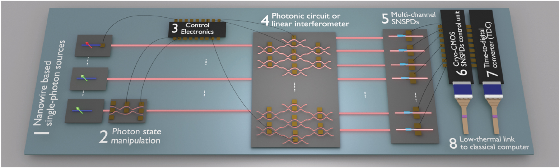
Illustration of an integrated nanowire-based photonic chip to be developed in the future. In this figure, optically excited nanowire QDs sources are shown in green arrows while the electrically pumped single-photon source is shown in red arrows; optical connections between different components are highlighted in pink lines, and electrical contacts are represented by orange squares; waveguide-integrated superconducting nanowire single-photon detectors are marked by cyan wires, and integrated control electronic circuits, for example, cryo-CMOS or TDCs, are shown in black rectangles with multiple bonding pads.
6.2 On-chip quantum bio-sensing
Different classes of single-photon emitters have been employed for bio-photonic imaging and spectroscopy. Each of these emitters has its own advantages and weaknesses. To this end, quantum dots were among the first emitters to be explored and have already come a long way. Most commonly in biomedical applications and fluorescence microscopy, quantum dots (and in general single-photon emitters) are utilized as biomarkers [192], [193], [194], [195], [196] in which their position (localization), color, brightness, lifetime, etc. is linked to a certain biological/chemical factor. Among the important remaining challenges ahead of bio-quantum sensing with quantum dots are chemical toxicity and optical attenuation, i.e. the light from the emitter is highly attenuated by the tissue before reaching the detection optics. Infrared quantum dots can benefit from enhanced transparency of the tissue. Synthesis of high-quality infrared emitting quantum dots [197, 198] as well as efficient and precise detection of those photons [199, 200] have achieved promising results but require further progress. High quantum yield emitters as well as sensitive and low noise detectors with a large active area can further boost the impact of infrared bio-imaging.
As described in the previous sections, integrated photonic circuits can generate, transmit, and detect a broad band of optical signals on-chip. This naturally offers the ability to simultaneously detect and identify different biological objects (e.g. single-virus [201], proteins [202], and single-molecule [203]), which is one of the key requirements for disease diagnostic and drug developments.
Integrated photonic circuits can help to create such a highly sensitive, multi-functional platform on a chip scale. Also, by using single-photon detectors, the sensitivity of such systems can be improved to reach their quantum limits. As depicted in Figure 10, a broadband excitation light signal transmits from free space to the chip with the help of efficient grating couplers. The waveguide delivers light to the samples under test (a virus in this case). Afterward, the transmitted or scattered photon signal pass through the meta-surface grating to acquire spectral information with multi-pixel SNSPDs at the detection ports. With precise spectral information, the identity or structure of bio-samples can be efficiently acquired. Such chips hold great potential in both scientific labs and biochemical industries, and again, nanowire-based devices are the key enabling elements in the proposed systems.

A proposed integrated quantum sensing chip for single-virus testing, including free space excitation laser, grating couplers, optical waveguide, the sample under test (single-virus as an example, can also be a single-molecule or protein, etc.), meta-surface grating, and multi-pixel SNSPDs.
7 Conclusion and future perspectives
With the 2022 Nobel physics prize awarded to the scientists who opened the quantum optics field using single-photons and entangled photon pairs, the field of quantum photonics science is expected to gain more attention. After decades of development, this field has witnessed great developments in both fundamental theory and real-world applications. The applications of nanowires QDs and SNSPDs are extending from proof-of-principle demonstrations to large-scale quantum computing, quantum simulation, and quantum sensing. Integrated and hybrid quantum photonic solutions are promising approaches for developing next-generation quantum hardware, where the advantages of photonics, electronics, and condensed matter physics can be combined for game-changing innovations. Looking into the future, there are still important challenges to be addressed:
From quantum emitters’ perspective, to interface the flying qubits with the current optical fiber network, quantum emitters must be developed that operate at the telecommunication wavelength around 1550 nm. A further benefit of this advancement is enabling hybrid integration to silicon on insulator photonics, the most developed photonic platform for both classical and quantum applications. Additionally, one key objective is to interface several nanowire QDs, so that they may be used as solid-state quantum memories, and each may function as a quantum node for communication purposes. Such target application would require Fourier-limited emission and more stringent control over the emission wavelength spread in nanowire quantum dot samples. Lastly, higher photon indistinguishability without time-gating or post-processing is key for several applications highlighted in this review.
On the detection side, significant advancements have recently been made, allowing SNSPDs to be used in new fields including biological imaging. Following this advancement, it may be advantageous to realize SNSPDs at longer wavelength ranges. This should be done in collaboration with researchers developing biological markers to maximize the detectors’ qualities in the desired wavelength range. Additionally, even though large-scale SNSPD arrays have made significant progress, additional work is still required to realize SNDPD 2D cameras with individual pixel-readout circuitry solutions. In the realms of optical imaging, sensing, and biology, this will be a game-changer. Also, a better understanding of how the superconducting films’ material properties influence their photon detection performance will help to improve SNSPDs’ yield, and ultimately bring down the cost of this technology. This will advance the commercialization of SNSPDs and expand their use to as-yet-untapped markets and research areas.
To conclude, through a systematic review of the theory, material platform, and fabrication process of the nanowires, this paper serves as a solid reference for both young and senior researchers in the integrated quantum photonics field. Additionally, we propose promising quantum photonics architectures and sensing experiments and aim at attracting a wider range of readers and invoking more collaboration between researchers in different fields.
Funding source: Vinnova quantum kick-start Project
Award Identifier / Grant number: 2021
Funding source: Knut and Alice Wallenberg (KAW) Foundation through the Wallenberg Centre for Quantum Technology (WACQT)
Funding source: D.A.S acknowledges support by the Australian Research Council
Award Identifier / Grant number: DE190100430
Funding source: Swedish Research Council (VR) Starting Grant
Award Identifier / Grant number: 2016-03905
Acknowledgments
A. W. E acknowledges support from the Knut and Alice Wallenberg (KAW) Foundation through the Wallenberg Centre for Quantum Technology (WACQT), Swedish Research Council (VR) Starting, and Vinnova quantum kick-start project 2021.
-
Author contributions: All the authors have accepted responsibility for the entire content of this submitted manuscript and approved submission.
-
Research funding: None declared.
-
Conflict of interest statement: The authors declare no conflicts of interest regarding this article.
References
[1] G. Grynberg, A. Aspect, C. Fabre, and C. Cohen-Tannoudji, Introduction to Quantum Optics: From the Semi-Classical Approach to Quantized Light, Cambridge, Cambridge University Press, 2010.10.1017/CBO9780511778261Search in Google Scholar
[2] C. Gerry and P. Knight, Introductory Quantum Optics, Cambridge, Cambridge University Press, 2004.10.1017/CBO9780511791239Search in Google Scholar
[3] M. Fox, Quantum Optics: An Introduction. Oxford Master Series in Physics, Oxford, OUP Oxford, 2006.Search in Google Scholar
[4] H. S. Zhong, H. Wang, Y. H. Deng, et al.., “Quantum computational advantage using photons,” Science, vol. 370, no. 6523, pp. 1460–1463, 2020. https://doi.org/10.1126/science.abe8770.Search in Google Scholar PubMed
[5] S. Tanzilli, A. Martin, F. Kaiser, M. P. De Micheli, O. Alibart, and D. B. Ostrowsky, “On the genesis and evolution of integrated quantum optics,” Laser Photon. Rev., vol. 6, no. 1, pp. 115–143, 2012. https://doi.org/10.1002/lpor.201100010.Search in Google Scholar
[6] F. Flamini, N. Spagnolo, and F. Sciarrino, “Photonic quantum information processing: a review,” Rep. Prog. Phys., vol. 82, no. 1, p. 016001, 2018. https://doi.org/10.1088/1361-6633/aad5b2.Search in Google Scholar PubMed
[7] A. W. Elshaari, W. Pernice, K. Srinivasan, O. Benson, and V. Zwiller, “Hybrid integrated quantum photonic circuits,” Nat. Photonics, vol. 14, no. 5, pp. 285–298, 2020. https://doi.org/10.1038/s41566-020-0609-x.Search in Google Scholar PubMed PubMed Central
[8] G. Moody, V. J. Sorger, D. J. Blumenthal, et al.., “2022 roadmap on integrated quantum photonics,” J. Phys. Photon., vol. 4, no. 1, p. 012501, 2022. https://doi.org/10.1088/2515-7647/ac1ef4.Search in Google Scholar
[9] J. Carolan, C. Harrold, C. Sparrow, et al.., “Universal linear optics,” Science, vol. 349, no. 6249, pp. 711–716, 2015. https://doi.org/10.1126/science.aab3642.Search in Google Scholar PubMed
[10] B. Bartlett and S. Fan, “Universal programmable photonic architecture for quantum information processing,” Phys. Rev. A, vol. 101, p. 042319, 2020. https://doi.org/10.1103/physreva.101.042319.Search in Google Scholar
[11] P. Lodahl, “Quantum-dot based photonic quantum networks,” Quantum Sci. Technol., vol. 3, no. 1, p. 013001, 2017. https://doi.org/10.1088/2058-9565/aa91bb.Search in Google Scholar
[12] B. J. Metcalf, J. B. Spring, P. C. Humphreys, et al.., “Quantum teleportation on a photonic chip,” Nat. Photonics, vol. 8, no. 10, pp. 770–774, 2014. https://doi.org/10.1038/nphoton.2014.217.Search in Google Scholar
[13] P. Zhang, K. Aungskunsiri, E. Martín-López, et al.., “Reference-frame-independent quantum-key-distribution server with a telecom tether for an on-chip client,” Phys. Rev. Lett., vol. 112, p. 130501, 2014. https://doi.org/10.1103/physrevlett.112.130501.Search in Google Scholar PubMed
[14] J. Wang, F. Sciarrino, A. Laing, and M. G. Thompson, “Integrated photonic quantum technologies,” Nat. Photonics, vol. 14, no. 5, pp. 273–284, 2020. https://doi.org/10.1038/s41566-019-0532-1.Search in Google Scholar
[15] M. D. Eisaman, J. Fan, A. Migdall, and S. V. Polyakov, “Invited review article: single-photon sources and detectors,” Rev. Sci. Instrum., vol. 82, no. 7, p. 071101, 2011. https://doi.org/10.1063/1.3610677.Search in Google Scholar PubMed
[16] E. Meyer-Scott, C. Silberhorn, and A. Migdall, “Single-photon sources: approaching the ideal through multiplexing,” Rev. Sci. Instrum., vol. 91, no. 4, p. 041101, 2020. https://doi.org/10.1063/5.0003320.Search in Google Scholar PubMed PubMed Central
[17] I. E. Zadeh, J. Chang, J. W. N. Los, et al.., “Superconducting nanowire single-photon detectors: a perspective on evolution, state-of-the-art, future developments, and applications,” Appl. Phys. Lett., vol. 118, no. 19, p. 190502, 2021. https://doi.org/10.1063/5.0045990.Search in Google Scholar
[18] I. Aharonovich, D. Englund, and M. Toth, “Solid-state single-photon emitters,” Nat. Photonics, vol. 10, no. 10, pp. 631–641, 2016. https://doi.org/10.1038/nphoton.2016.186.Search in Google Scholar
[19] X. He, H. Htoon, S. K. Doorn, et al.., “Carbon nanotubes as emerging quantum-light sources,” Nat. Mater., vol. 17, no. 8, pp. 663–670, 2018. https://doi.org/10.1038/s41563-018-0109-2.Search in Google Scholar PubMed
[20] Y. Arakawa and M. J. Holmes, “Progress in quantum-dot single photon sources for quantum information technologies: a broad spectrum overview,” Appl. Phys. Rev., vol. 7, no. 2, p. 021309, 2020. https://doi.org/10.1063/5.0010193.Search in Google Scholar
[21] M. Toth and I. Aharonovich, “Single photon sources in atomically thin materials,” Annu. Rev. Phys. Chem., vol. 70, pp. 123–142, 2019. https://doi.org/10.1146/annurev-physchem-042018-052628.Search in Google Scholar PubMed
[22] N. Somaschi, V. Giesz, L. De Santis, et al.., “Near-optimal single-photon sources in the solid state,” Nat. Photonics, vol. 10, no. 5, pp. 340–345, 2016. https://doi.org/10.1038/nphoton.2016.23.Search in Google Scholar
[23] N. Tomm, A. Javadi, N. O. Antoniadis, et al.., “A bright and fast source of coherent single photons,” Nat. Nanotechnol., vol. 16, no. 4, pp. 399–403, 2021. https://doi.org/10.1038/s41565-020-00831-x.Search in Google Scholar PubMed
[24] L. Schweickert, K. D. Jöns, K. D. Zeuner, et al.., “On-demand generation of background-free single photons from a solid-state source,” Appl. Phys. Lett., vol. 112, no. 9, p. 093106, 2018. https://doi.org/10.1063/1.5020038.Search in Google Scholar
[25] X. Ding, Y. He, Z. C. Duan, et al.., “On-demand single photons with high extraction efficiency and near-unity indistinguishability from a resonantly driven quantum dot in a micropillar,” Phys. Rev. Lett., vol. 116, no. 2, p. 020401, 2016. https://doi.org/10.1103/physrevlett.116.020401.Search in Google Scholar
[26] H. Wang, Y. He, Y. H. Li, et al.., “High-efficiency multiphoton boson sampling,” Nat. Photonics, vol. 11, no. 6, pp. 361–365, 2017. https://doi.org/10.1038/nphoton.2017.63.Search in Google Scholar
[27] M. E. Reimer, G. Bulgarini, N. Akopian, et al.., “Bright single-photon sources in bottom-up tailored nanowires,” Nat. Commun., vol. 3, no. 1, pp. 1–6, 2012. https://doi.org/10.1038/ncomms1746.Search in Google Scholar PubMed PubMed Central
[28] R. Singh and G. Bester, “Nanowire quantum dots as an ideal source of entangled photon pairs,” Phys. Rev. Lett., vol. 103, no. 6, p. 063601, 2009. https://doi.org/10.1103/physrevlett.103.063601.Search in Google Scholar
[29] M. A. M. Versteegh, M. E. Reimer, K. D. Jöns, et al.., “Observation of strongly entangled photon pairs from a nanowire quantum dot,” Nat. Commun., vol. 5, no. 1, pp. 1–6, 2014. https://doi.org/10.1038/ncomms6298.Search in Google Scholar PubMed PubMed Central
[30] P. Laferrière, A. Yin, E. Yeung, et al.., “Approaching transform-limited photons from nanowire quantum dots excited above-band,” arXiv preprint arXiv:2208.00066, 2022.10.1103/PhysRevB.107.155422Search in Google Scholar
[31] D. Dalacu, P. J. Poole, and R. L. Williams, “Nanowire-based sources of non-classical light,” Nanotechnology, vol. 30, no. 23, p. 232001, 2019. https://doi.org/10.1088/1361-6528/ab0393.Search in Google Scholar PubMed
[32] R. G. Hobbs, N. Petkov, and J. D. Holmes, “Semiconductor nanowire fabrication by bottom-up and top-down paradigms,” Chem. Mater., vol. 24, no. 11, p. 1975–1991, 2012. https://doi.org/10.1021/cm300570n.Search in Google Scholar
[33] P. Laferrière, E. Yeung, I. Miron, et al.., “Unity yield of deterministically positioned quantum dot single photon sources,” Sci. Rep., vol. 12, no. 1, pp. 1–9, 2022. https://doi.org/10.1038/s41598-022-10451-1.Search in Google Scholar PubMed PubMed Central
[34] S. Haffouz, K. D. Zeuner, D. Dalacu, et al.., “Bright single inasp quantum dots at telecom wavelengths in position-controlled inp nanowires: the role of the photonic waveguide,” Nano Lett., vol. 18, no. 5, pp. 3047–3052, 2018. https://doi.org/10.1021/acs.nanolett.8b00550.Search in Google Scholar PubMed
[35] G. Bulgarini, M. E. Reimer, M. B. Bavinck, et al.., “Nanowire waveguides launching single photons in a Gaussian mode for ideal fiber coupling,” Nano Lett., vol. 14, no. 7, pp. 4102–4106, 2014. https://doi.org/10.1021/nl501648f.Search in Google Scholar PubMed
[36] P. Laferriere, E. Yeung, L. Giner, et al.., “Multiplexed single-photon source based on multiple quantum dots embedded within a single nanowire,” Nano Lett., vol. 20, no. 5, pp. 3688–3693, 2020. https://doi.org/10.1021/acs.nanolett.0c00607.Search in Google Scholar PubMed
[37] A. W. Elshaari, I. E. Zadeh, A. Fognini, et al.., “On-chip single photon filtering and multiplexing in hybrid quantum photonic circuits,” Nat. Commun., vol. 8, no. 1, pp. 1–8, 2017. https://doi.org/10.1038/s41467-017-00486-8.Search in Google Scholar PubMed PubMed Central
[38] A. W. Elshaari, E. Büyüközer, I. E. Zadeh, et al.., “Strain-tunable quantum integrated photonics,” Nano Lett., vol. 18, no. 12, pp. 7969–7976, 2018. https://doi.org/10.1021/acs.nanolett.8b03937.Search in Google Scholar PubMed PubMed Central
[39] M. Zeeshan, N. Sherlekar, A. Ahmadi, R. L. Williams, and M. E. Reimer, “Proposed scheme to generate bright entangled photon pairs by application of a quadrupole field to a single quantum dot,” Phys. Rev. Lett., vol. 122, no. 22, p. 227401, 2019. https://doi.org/10.1103/physrevlett.122.227401.Search in Google Scholar PubMed
[40] F. Liu, A. J. Brash, J. O’Hara, et al.., “High purcell factor generation of indistinguishable on-chip single photons,” Nat. Nanotechnol., vol. 13, no. 9, pp. 835–840, 2018. https://doi.org/10.1038/s41565-018-0188-x.Search in Google Scholar PubMed
[41] K. G. Lagoudakis, P. L. McMahon, K. A. Fischer, et al.., “Initialization of a spin qubit in a site-controlled nanowire quantum dot,” New J. Phys., vol. 18, no. 5, p. 053024, 2016. https://doi.org/10.1088/1367-2630/18/5/053024.Search in Google Scholar
[42] P. Aumann, M. Prilmüller, F. Kappe, et al.., “Demonstration and modeling of time-bin entangled photons from a quantum dot in a nanowire,” AIP Adv., vol. 12, no. 5, p. 055115, 2022. https://doi.org/10.1063/5.0081874.Search in Google Scholar
[43] P. Anderson, R. Al Maruf, S. Venuturumilli, et al.., “Delaying tunable single photons from a quantum dot with an atomic ensemble,” in APS Division of Atomic, Molecular and Optical Physics Meeting Abstracts, vol. 2022, 2022, pp. F01–F047.Search in Google Scholar
[44] R. Al Maruf, S. S. Venuturumilli, D. Bharadwaj, et al.., “Single-photon source based on a quantum dot emitting at cesium wavelength,” in Optical and Quantum Sensing and Precision Metrology II, vol. 12016, Bellingham, WA, USA, SPIE, 2022, pp. 239–246.10.1117/12.2616977Search in Google Scholar
[45] D. Bharadwaj, P. Anderson, S. Venuturumilli, et al.., “Interfacing quantum dots with laser-cooled atomic ensembles,” in Optical and Quantum Sensing and Precision Metrology, vol. 11700, Bellingham, WA, USA, SPIE, 2021, pp. 211–217.10.1117/12.2586902Search in Google Scholar
[46] Y. Chen, I. E. Zadeh, K. D. Jöns, et al.., “Controlling the exciton energy of a nanowire quantum dot by strain fields,” Appl. Phys. Lett., vol. 108, no. 18, p. 182103, 2016. https://doi.org/10.1063/1.4948762.Search in Google Scholar
[47] J. C. Blakesley, P. See, A. J. Shields, et al.., “Efficient single photon detection by quantum dot resonant tunneling diodes,” Phys. Rev. Lett., vol. 94, p. 067401, 2005. https://doi.org/10.1103/physrevlett.94.067401.Search in Google Scholar
[48] M. J. Grotevent, C. U. Hail, S. Yakunin, et al.., “Colloidal hgte quantum dot/graphene phototransistor with a spectral sensitivity beyond 3 μm,” Adv. Sci., vol. 8, no. 6, p. 2003360, 2021. https://doi.org/10.1002/advs.202003360.Search in Google Scholar PubMed PubMed Central
[49] S. J. Gibson, B. van Kasteren, B. Tekcan, et al.., “Tapered inp nanowire arrays for efficient broadband high-speed single-photon detection,” Nat. Nanotechnol., vol. 14, no. 5, pp. 473–479, 2019. https://doi.org/10.1038/s41565-019-0393-2.Search in Google Scholar PubMed
[50] L. Cao, J. S. Park, P. Fan, B. Clemens, and M. L. Brongersma, “Resonant germanium nanoantenna photodetectors,” Nano Lett., vol. 10, no. 4, pp. 1229–1233, 2010. https://doi.org/10.1021/nl9037278.Search in Google Scholar PubMed
[51] G. Bulgarini, M. E. Reimer, M. Hocevar, E. P. A. M. Bakkers, L. P. Kouwenhoven, and V. Zwiller, “Avalanche amplification of a single exciton in a semiconductor nanowire,” Nat. Photonics, vol. 6, no. 7, pp. 455–458, 2012. https://doi.org/10.1038/nphoton.2012.110.Search in Google Scholar
[52] G. N. Gol’Tsman, O. Okunev, G. Chulkova, et al.., “Picosecond superconducting single-photon optical detector,” Appl. Phys. Lett., vol. 79, no. 6, pp. 705–707, 2001. https://doi.org/10.1063/1.1388868.Search in Google Scholar
[53] C. M. Natarajan, M. G. Tanner, and R. H. Hadfield, “Superconducting nanowire single-photon detectors: physics and applications,” Supercond. Sci. Technol., vol. 25, no. 6, p. 063001, 2012. https://doi.org/10.1088/0953-2048/25/6/063001.Search in Google Scholar
[54] H. S. Zhong, Y. H. Deng, J. Qin, et al.., “Phase-programmable Gaussian boson sampling using stimulated squeezed light,” Phys. Rev. Lett., vol. 127, no. 18, p. 180502, 2021. https://doi.org/10.1103/physrevlett.127.180502.Search in Google Scholar
[55] O. Kahl, S. Ferrari, V. Kovalyuk, G. N. Goltsman, A. Korneev, and W. H. P. Pernice, “Waveguide integrated superconducting single-photon detectors with high internal quantum efficiency at telecom wavelengths,” Sci. Rep., vol. 5, no. 1, pp. 1–11, 2015. https://doi.org/10.1038/srep10941.Search in Google Scholar PubMed PubMed Central
[56] M. A. Wolff, S. Vogel, L. Splitthoff, and C. Schuck, “Superconducting nanowire single-photon detectors integrated with tantalum pentoxide waveguides,” Sci. Rep., vol. 10, no. 1, pp. 1–9, 2020. https://doi.org/10.1038/s41598-020-74426-w.Search in Google Scholar PubMed PubMed Central
[57] R. Gourgues, I. E. Zadeh, A. W. Elshaari, et al.., “Controlled integration of selected detectors and emitters in photonic integrated circuits,” Opt. Express, vol. 27, no. 3, pp. 3710–3716, 2019. https://doi.org/10.1364/oe.27.003710.Search in Google Scholar PubMed
[58] J. Münzberg, A. Vetter, F. Beutel, et al.., “Superconducting nanowire single-photon detector implemented in a 2d photonic crystal cavity,” Optica, vol. 5, no. 5, pp. 658–665, 2018. https://doi.org/10.1364/optica.5.000658.Search in Google Scholar
[59] A. Vetter, S. Ferrari, P. Rath, et al.., “Cavity-enhanced and ultrafast superconducting single-photon detectors,” Nano Lett., vol. 16, no. 11, pp. 7085–7092, 2016. https://doi.org/10.1021/acs.nanolett.6b03344.Search in Google Scholar PubMed
[60] M. K. Akhlaghi, E. Schelew, and J. F. Young, “Waveguide integrated superconducting single-photon detectors implemented as near-perfect absorbers of coherent radiation,” Nat. Commun., vol. 6, no. 1, pp. 1–8, 2015. https://doi.org/10.1038/ncomms9233.Search in Google Scholar PubMed
[61] J. Chang, J. W. N. Los, J. O. Tenorio-Pearl, et al.., “Detecting telecom single photons with 99.5− 2.07+ 0.5% system detection efficiency and high time resolution,” APL Photonics, vol. 6, no. 3, p. 036114, 2021. https://doi.org/10.1063/5.0039772.Search in Google Scholar
[62] J. P. Sprengers, A. Gaggero, D. Sahin, et al.., “Waveguide superconducting single-photon detectors for integrated quantum photonic circuits,” Appl. Phys. Lett., vol. 99, no. 18, p. 181110, 2011. https://doi.org/10.1063/1.3657518.Search in Google Scholar
[63] W. H. P. Pernice, C. Schuck, O. Minaeva, et al.., “High-speed and high-efficiency travelling wave single-photon detectors embedded in nanophotonic circuits,” Nat. Commun., vol. 3, no. 1, pp. 1–10, 2012. https://doi.org/10.1038/ncomms2307.Search in Google Scholar PubMed PubMed Central
[64] S. Ferrari, C. Schuck, and W. Pernice, “Waveguide-integrated superconducting nanowire single-photon detectors,” Nanophotonics, vol. 7, no. 11, pp. 1725–1758, 2018. https://doi.org/10.1515/nanoph-2018-0059.Search in Google Scholar
[65] B. A. Joyce, “Molecular beam epitaxy,” Rep. Prog. Phys., vol. 48, no. 12, p. 1637, 1985. https://doi.org/10.1088/0034-4885/48/12/002.Search in Google Scholar
[66] M. R. Leys and H. Veenvliet, “A study of the growth mechanism of epitaxial gaas as grown by the technique of metal organic vapour phase epitaxy,” J. Cryst. Growth, vol. 55, no. 1, pp. 145–153, 1981. https://doi.org/10.1016/0022-0248(81)90282-7.Search in Google Scholar
[67] H. Mäntynen, N. Anttu, Z. Sun, and H. Lipsanen, “Single-photon sources with quantum dots in iii–v nanowires,” Nanophotonics, vol. 8, no. 5, pp. 747–769, 2019. https://doi.org/10.1515/nanoph-2019-0007.Search in Google Scholar
[68] J. Zichi, J. Chang, S. Steinhauer, et al.., “Optimizing the stoichiometry of ultrathin nbtin films for high-performance superconducting nanowire single-photon detectors,” Opt. Express, vol. 27, no. 19, pp. 26579–26587, 2019. https://doi.org/10.1364/oe.27.026579.Search in Google Scholar PubMed
[69] A. Cavalli, J. Wang, I. E. Zadeh, et al.., “High-yield growth and characterization of ⟨100⟩ inp p–n diode nanowires,” Nano Lett., vol. 16, no. 5, pp. 3071–3077, 2016. https://doi.org/10.1021/acs.nanolett.6b00203.Search in Google Scholar PubMed
[70] I. E. Zadeh, A. W. Elshaari, K. D. Jöns, et al.., “Deterministic integration of single photon sources in silicon based photonic circuits,” Nano Lett., vol. 16, no. 4, pp. 2289–2294, 2016. https://doi.org/10.1021/acs.nanolett.5b04709.Search in Google Scholar PubMed
[71] K. Mnaymneh, D. Dalacu, J. McKee, et al.., “On-chip integration of single photon sources via evanescent coupling of tapered nanowires to sin waveguides,” Adv. Quantum Technol., vol. 3, no. 2, p. 1900021, 2020. https://doi.org/10.1002/qute.201900021.Search in Google Scholar
[72] L. Yang, S. Steinhauer, E. Strambini, et al.., “Proximitized josephson junctions in highly-doped inas nanowires robust to optical illumination,” Nanotechnology, vol. 32, no. 7, p. 075001, 2020. https://doi.org/10.1088/1361-6528/abc44e.Search in Google Scholar PubMed
[73] A. Osada, Y. Ota, R. Katsumi, M. Kakuda, S. Iwamoto, and Y. Arakawa, “Strongly coupled single-quantum-dot–cavity system integrated on a cmos-processed silicon photonic chip,” Phys. Rev. Appl., vol. 11, no. 2, p. 024071, 2019. https://doi.org/10.1103/physrevapplied.11.024071.Search in Google Scholar
[74] R. Katsumi, Y. Ota, M. Kakuda, S. Iwamoto, and Y. Arakawa, “Transfer-printed single-photon sources coupled to wire waveguides,” Optica, vol. 5, no. 6, pp. 691–694, 2018. https://doi.org/10.1364/optica.5.000691.Search in Google Scholar
[75] M. Davanco, J. Liu, L. Sapienza, et al.., “Heterogeneous integration for on-chip quantum photonic circuits with single quantum dot devices,” Nat. Commun., vol. 8, no. 1, pp. 1–12, 2017. https://doi.org/10.1038/s41467-017-00987-6.Search in Google Scholar PubMed PubMed Central
[76] J. H. Kim, S. Aghaeimeibodi, J. Carolan, D. Englund, and E. Waks, “Hybrid integration methods for on-chip quantum photonics,” Optica, vol. 7, no. 4, pp. 291–308, 2020. https://doi.org/10.1364/optica.384118.Search in Google Scholar
[77] B. Alloing, C. Zinoni, V. Zwiller, et al.., “Growth and characterization of single quantum dots emitting at 1300 nm,” Appl. Phys. Lett., vol. 86, no. 10, p. 101908, 2005. https://doi.org/10.1063/1.1872213.Search in Google Scholar
[78] D. Dalacu, K. Mnaymneh, J. Lapointe, et al.., “Ultraclean emission from inasp quantum dots in defect-free wurtzite inp nanowires,” Nano Lett., vol. 12, no. 11, pp. 5919–5923, 2012. https://doi.org/10.1021/nl303327h.Search in Google Scholar PubMed
[79] M. T. Borgström, V. Zwiller, E. Müller, and A. Imamoglu, “Optically bright quantum dots in single nanowires,” Nano Lett., vol. 5, no. 7, pp. 1439–1443, 2005. https://doi.org/10.1021/nl050802y.Search in Google Scholar PubMed
[80] S. Deshpande, J. Heo, A. Das, and P. Bhattacharya, “Electrically driven polarized single-photon emission from an ingan quantum dot in a gan nanowire,” Nat. Commun., vol. 4, no. 1, pp. 1–8, 2013. https://doi.org/10.1038/ncomms2691.Search in Google Scholar PubMed
[81] P. Mrowiński, A. Musiał, K. Gawarecki, et al.., “Excitonic complexes in mocvd-grown ingaas/gaas quantum dots emitting at telecom wavelengths,” Phys. Rev. B, vol. 100, no. 11, p. 115310, 2019. https://doi.org/10.1103/physrevb.100.115310.Search in Google Scholar
[82] M. J. Holmes, K. Choi, S. Kako, M. Arita, and Y. Arakawa, “Room-temperature triggered single photon emission from a iii-nitride site-controlled nanowire quantum dot,” Nano Lett., vol. 14, no. 2, pp. 982–986, 2014. https://doi.org/10.1021/nl404400d.Search in Google Scholar PubMed
[83] R. Cheng, J. Wright, H. G. Xing, D. Jena, and H. X. Tang, “Epitaxial niobium nitride superconducting nanowire single-photon detectors,” Appl. Phys. Lett., vol. 117, no. 13, p. 132601, 2020. https://doi.org/10.1063/5.0018818.Search in Google Scholar
[84] G. G. Taylor, D. V. Morozov, C. T. Lennon, P. S. Barry, C. Sheagren, and R. H. Hadfield, “Infrared single-photon sensitivity in atomic layer deposited superconducting nanowires,” Appl. Phys. Lett., vol. 118, no. 19, p. 191106, 2021. https://doi.org/10.1063/5.0048799.Search in Google Scholar
[85] I. E. Zadeh, J. W. N. Los, R. B. M. Gourgues, et al.., “Efficient single-photon detection with 7.7 ps time resolution for photon-correlation measurements,” ACS Photonics, vol. 7, no. 7, pp. 1780–1787, 2020. https://doi.org/10.1021/acsphotonics.0c00433.Search in Google Scholar
[86] F. Marsili, V. B. Verma, J. A. Stern, et al.., “Detecting single infrared photons with 93% system efficiency,” Nat. Photonics, vol. 7, no. 3, pp. 210–214, 2013. https://doi.org/10.1038/nphoton.2013.13.Search in Google Scholar
[87] D. V. Reddy, R. R. Nerem, S. W. Nam, R. P. Mirin, and V. B. Verma, “Superconducting nanowire single-photon detectors with 98% system detection efficiency at 1550 nm,” Optica, vol. 7, no. 12, pp. 1649–1653, 2020. https://doi.org/10.1364/optica.400751.Search in Google Scholar
[88] C. Cirillo, J. Chang, M. Caputo, et al.., “Superconducting nanowire single photon detectors based on disordered nbre films,” Appl. Phys. Lett., vol. 117, no. 17, p. 172602, 2020. https://doi.org/10.1063/5.0021487.Search in Google Scholar
[89] C. Yang, M. Si, X. Zhang, et al.., “Large-area tan superconducting microwire single photon detectors for x-ray detection,” Opt. Express, vol. 29, no. 14, pp. 21400–21408, 2021. https://doi.org/10.1364/oe.422581.Search in Google Scholar PubMed
[90] P. Hu, H. Li, L. You, et al.., “Detecting single infrared photons toward optimal system detection efficiency,” Opt. Express, vol. 28, no. 24, pp. 36884–36891, 2020. https://doi.org/10.1364/oe.410025.Search in Google Scholar
[91] S. Cherednichenko, N. Acharya, E. Novoselov, and V. Drakinskiy, “Low kinetic inductance superconducting mgb2 nanowires with a 130 ps relaxation time for single-photon detection applications,” Supercond. Sci. Technol., vol. 34, no. 4, p. 044001, 2021. https://doi.org/10.1088/1361-6668/abdeda.Search in Google Scholar
[92] J. Marks, J. O. N. L. Schindler, and C. A. R. L. R. Kannewurf, “Metalorganic chemical vapor deposition,” in MRS Online Proceedings Library (OPL), 1982.Search in Google Scholar
[93] J. Li, R. A. Kirkwood, L. J. Baker, et al.., “Nano-optical single-photon response mapping of waveguide integrated molybdenum silicide (mosi) superconducting nanowires,” Opt. Express, vol. 24, no. 13, pp. 13931–13938, 2016. https://doi.org/10.1364/oe.24.013931.Search in Google Scholar PubMed
[94] J. B. Spring, B. J. Metcalf, P. C. Humphreys, et al.., “Boson sampling on a photonic chip,” Science, vol. 339, no. 6121, pp. 798–801, 2013. https://doi.org/10.1126/science.1231692.Search in Google Scholar PubMed
[95] H. Wang, J. Qin, X. Ding, et al.., “Boson sampling with 20 input photons and a 60-mode interferometer in a 1 0 14-dimensional hilbert space,” Phys. Rev. Lett., vol. 123, no. 25, p. 250503, 2019. https://doi.org/10.1103/physrevlett.123.250503.Search in Google Scholar PubMed
[96] S. Paesani, Y. Ding, R. Santagati, et al.., “Generation and sampling of quantum states of light in a silicon chip,” Nat. Phys., vol. 15, no. 9, pp. 925–929, 2019. https://doi.org/10.1038/s41567-019-0567-8.Search in Google Scholar
[97] S. Aaronson and A. Arkhipov, “The computational complexity of linear optics,” Theor. Comput., vol. 9, no. 4, pp. 143–252, 2013. https://doi.org/10.4086/toc.2013.v009a004.Search in Google Scholar
[98] D. J. Brod, E. F. Galvão, A. Crespi, R. Osellame, N. Spagnolo, and F. Sciarrino, “Photonic implementation of boson sampling: a review,” Adv. Photonics, vol. 1, no. 3, p. 034001, 2019.Search in Google Scholar
[99] M. A. Broome, A. Fedrizzi, S. Rahimi-Keshari et al.., “Photonic boson sampling in a tunable circuit,” Science, vol. 339, no. 6121, pp. 794–798, 2013. https://doi.org/10.1126/science.1231440.Search in Google Scholar PubMed
[100] M. Tillmann, B. Dakić, R. Heilmann, S. Nolte, A. Szameit, and P. Walther, “Experimental boson sampling,” Nat. Photonics, vol. 7, no. 7, pp. 540–544, 2013. https://doi.org/10.1038/nphoton.2013.102.Search in Google Scholar
[101] A. Crespi, R. Osellame, R. Ramponi, et al.., “Integrated multimode interferometers with arbitrary designs for photonic boson sampling,” Nat. Photonics, vol. 7, no. 7, pp. 545–549, 2013. https://doi.org/10.1038/nphoton.2013.112.Search in Google Scholar
[102] J. C. Loredo, M. A. Broome, P. Hilaire, et al.., “Boson sampling with single-photon fock states from a bright solid-state source,” Phys. Rev. Lett., vol. 118, no. 13, p. 130503, 2017. https://doi.org/10.1103/physrevlett.118.130503.Search in Google Scholar
[103] C. S. Hamilton, R. Kruse, L. Sansoni, S. Barkhofen, C. Silberhorn, and I. Jex, “Gaussian boson sampling,” Phys. Rev. Lett., vol. 119, no. 17, p. 170501, 2017. https://doi.org/10.1103/physrevlett.119.170501.Search in Google Scholar
[104] R. Kruse, C. S. Hamilton, L. Sansoni, S. Barkhofen, C. Silberhorn, and I. Jex, “Detailed study of Gaussian boson sampling,” Phys. Rev. A, vol. 100, no. 3, p. 032326, 2019. https://doi.org/10.1103/physreva.100.032326.Search in Google Scholar
[105] S. Paesani, M. Borghi, S. Signorini, A. Maïnos, L. Pavesi, and L. Anthony, “Near-ideal spontaneous photon sources in silicon quantum photonics,” Nat. Commun., vol. 11, no. 1, pp. 1–6, 2020. https://doi.org/10.1038/s41467-020-16187-8.Search in Google Scholar PubMed PubMed Central
[106] J. W. Silverstone, R. Santagati, D. Bonneau, et al.., “Qubit entanglement between ring-resonator photon-pair sources on a silicon chip,” Nat. Commun., vol. 6, no. 1, pp. 1–7, 2015. https://doi.org/10.1038/ncomms8948.Search in Google Scholar PubMed PubMed Central
[107] V. D. Vaidya, B. Morrison, L. G. Helt, et al.., “Broadband quadrature-squeezed vacuum and nonclassical photon number correlations from a nanophotonic device,” Sci. Adv., vol. 6, no. 39, p. eaba9186, 2020. https://doi.org/10.1126/sciadv.aba9186.Search in Google Scholar PubMed PubMed Central
[108] L. You, “Superconducting nanowire single-photon detectors for quantum information,” Nanophotonics, vol. 9, no. 9, pp. 2673–2692, 2020. https://doi.org/10.1515/nanoph-2020-0186.Search in Google Scholar
[109] J. Huh, G. G. Guerreschi, B. Peropadre, J. R. McClean, and A. Aspuru-Guzik, “Boson sampling for molecular vibronic spectra,” Nat. Photonics, vol. 9, no. 9, pp. 615–620, 2015. https://doi.org/10.1038/nphoton.2015.153.Search in Google Scholar
[110] K. Brádler, P. L. Dallaire-Demers, P. Rebentrost, D. Su, and C. Weedbrook, “Gaussian boson sampling for perfect matchings of arbitrary graphs,” Phys. Rev. A, vol. 98, no. 3, p. 032310, 2018. https://doi.org/10.1103/physreva.98.032310.Search in Google Scholar
[111] J. M. Arrazola and T. R. Bromley, “Using Gaussian boson sampling to find dense subgraphs,” Phys. Rev. Lett., vol. 121, no. 3, p. 030503, 2018. https://doi.org/10.1103/physrevlett.121.030503.Search in Google Scholar PubMed
[112] L. Banchi, M. Fingerhuth, T. Babej, C. Ing, and J. M. Arrazola, “Molecular docking with Gaussian boson sampling,” Sci. Adv., vol. 6, no. 23, p. eaax1950, 2020. https://doi.org/10.1126/sciadv.aax1950.Search in Google Scholar PubMed PubMed Central
[113] J. M. Arrazola, V. Bergholm, K. Brádler, et al.., “Quantum circuits with many photons on a programmable nanophotonic chip,” Nature, vol. 591, no. 7848, pp. 54–60, 2021. https://doi.org/10.1038/s41586-021-03202-1.Search in Google Scholar PubMed PubMed Central
[114] P. L. Mennea, W. R. Clements, D. H. Smith, et al.., “Modular linear optical circuits,” Optica, vol. 5, no. 9, pp. 1087–1090, 2018. https://doi.org/10.1364/optica.5.001087.Search in Google Scholar
[115] H. Tang, C. Di Franco, Z. Y. Shi, et al.., “Experimental quantum fast hitting on hexagonal graphs,” Nat. Photonics, vol. 12, no. 12, pp. 754–758, 2018. https://doi.org/10.1038/s41566-018-0282-5.Search in Google Scholar
[116] A. Peruzzo, M. Lobino, J. C. F. Matthews, et al.., “Quantum walks of correlated photons,” Science, vol. 329, no. 5998, pp. 1500–1503, 2010. https://doi.org/10.1126/science.1193515.Search in Google Scholar PubMed
[117] X. Qiang, Y. Wang, S. Xue, et al.., “Implementing graph-theoretic quantum algorithms on a silicon photonic quantum walk processor,” Sci. Adv., vol. 7, no. 9, p. eabb8375, 2021. https://doi.org/10.1126/sciadv.abb8375.Search in Google Scholar PubMed PubMed Central
[118] Y. Wang, Y. Liu, J. Zhan, et al.., “Large-scale full-programmable quantum walk and its applications,” arXiv preprint arXiv:2208.13186, 2022.Search in Google Scholar
[119] Y. Aharonov, L. Davidovich, and N. Zagury, “Quantum random walks,” Phys. Rev. A, vol. 48, no. 2, p. 1687, 1993. https://doi.org/10.1103/physreva.48.1687.Search in Google Scholar PubMed
[120] A. M. Childs, R. Cleve, E. Deotto, E. Farhi, S. Gutmann, and D. A. Spielman, “Exponential algorithmic speedup by a quantum walk,” in Proceedings of the Thirty-Fifth Annual ACM Symposium on Theory of Computing, 2003, pp. 59–68.10.1145/780542.780552Search in Google Scholar
[121] A. M. Childs and J. Goldstone, “Spatial search by quantum walk,” Phys. Rev. A, vol. 70, no. 2, p. 022314, 2004. https://doi.org/10.1103/physreva.70.022314.Search in Google Scholar
[122] C. Benedetti, D. Tamascelli, M. G. A. Paris, and A. Crespi, “Quantum spatial search in two-dimensional waveguide arrays,” Phys. Rev. Appl., vol. 16, no. 5, p. 054036, 2021. https://doi.org/10.1103/physrevapplied.16.054036.Search in Google Scholar
[123] J. Kempe, “Quantum random walks: an introductory overview,” Contemp. Phys., vol. 44, no. 4, pp. 307–327, 2003. https://doi.org/10.1080/00107151031000110776.Search in Google Scholar
[124] A. M. Childs, “Universal computation by quantum walk,” Phys. Rev. Lett., vol. 102, no. 18, p. 180501, 2009. https://doi.org/10.1103/physrevlett.102.180501.Search in Google Scholar
[125] A. M. Childs, D. Gosset, and Z. Webb, “Universal computation by multiparticle quantum walk,” Science, vol. 339, no. 6121, pp. 791–794, 2013. https://doi.org/10.1126/science.1229957.Search in Google Scholar PubMed
[126] M. A. Broome, A. Fedrizzi, B. P. Lanyon, I. Kassal, A. Aspuru-Guzik, and A. G. White, “Discrete single-photon quantum walks with tunable decoherence,” Phys. Rev. Lett., vol. 104, no. 15, p. 153602, 2010. https://doi.org/10.1103/physrevlett.104.153602.Search in Google Scholar
[127] A. Schreiber, K. N. Cassemiro, V. Potoček, et al.., “Photons walking the line: a quantum walk with adjustable coin operations,” Phys. Rev. Lett., vol. 104, no. 5, p. 050502, 2010. https://doi.org/10.1103/physrevlett.104.050502.Search in Google Scholar
[128] A. Schreiber, A. Gábris, P. P. Rohde, et al.., “A 2d quantum walk simulation of two-particle dynamics,” Science, vol. 336, no. 6077, pp. 55–58, 2012. https://doi.org/10.1126/science.1218448.Search in Google Scholar PubMed
[129] H. Tang, X. F. Lin, Z. Feng, et al.., “Experimental two-dimensional quantum walk on a photonic chip,” Sci. Adv., vol. 4, no. 5, p. eaat3174, 2018. https://doi.org/10.1126/sciadv.aat3174.Search in Google Scholar PubMed PubMed Central
[130] Z. Q. Jiao, J. Gao, W. H. Zhou, et al.., “Two-dimensional quantum walks of correlated photons,” Optica, vol. 8, no. 9, pp. 1129–1135, 2021. https://doi.org/10.1364/optica.425879.Search in Google Scholar
[131] P. Sibson, C. Erven, M. Godfrey, et al.., “Chip-based quantum key distribution,” Nat. Commun., vol. 8, no. 1, pp. 1–6, 2017. https://doi.org/10.1038/ncomms13984.Search in Google Scholar PubMed PubMed Central
[132] H. Semenenko, P. Sibson, A. Hart, M. G. Thompson, J. G. Rarity, and C. Erven, “Chip-based measurement-device-independent quantum key distribution,” Optica, vol. 7, no. 3, pp. 238–242, 2020. https://doi.org/10.1364/optica.379679.Search in Google Scholar
[133] F. Beutel, H. Gehring, M. A. Wolff, C. Schuck, and W. Pernice, “Detector-integrated on-chip qkd receiver for ghz clock rates,” Npj Quantum Inf., vol. 7, no. 1, pp. 1–8, 2021. https://doi.org/10.1038/s41534-021-00373-7.Search in Google Scholar
[134] F. Beutel, F. Brückerhoff-Plückelmann, H. Gehring, et al.., “Fully integrated four-channel wavelength-division multiplexed qkd receiver,” Optica, vol. 9, no. 10, pp. 1121–1130, 2022. https://doi.org/10.1364/optica.468982.Search in Google Scholar
[135] J. Yin, Y. Cao, Y. H. Li, et al.., “Satellite-based entanglement distribution over 1200 kilometers,” Science, vol. 356, no. 6343, pp. 1140–1144, 2017. https://doi.org/10.1126/science.aan3211.Search in Google Scholar PubMed
[136] S. K. Liao, W. Q. Cai, W. Y. Liu, et al.., “Satellite-to-ground quantum key distribution,” Nature, vol. 549, no. 7670, pp. 43–47, 2017. https://doi.org/10.1038/nature23655.Search in Google Scholar PubMed
[137] J. G. Ren, P. Xu, H. L. Yong, et al.., “Ground-to-satellite quantum teleportation,” Nature, vol. 549, no. 7670, pp. 70–73, 2017. https://doi.org/10.1038/nature23675.Search in Google Scholar PubMed
[138] S. K. Liao, W. Q. Cai, J. Handsteiner, et al.., “Satellite-relayed intercontinental quantum network,” Phys. Rev. Lett., vol. 120, no. 3, p. 030501, 2018. https://doi.org/10.1103/physrevlett.120.030501.Search in Google Scholar PubMed
[139] T. K. Paraiso, T. Roger, D. G. Marangon, et al.., “A photonic integrated quantum secure communication system,” Nat. Photonics, vol. 15, no. 11, pp. 850–856, 2021. https://doi.org/10.1038/s41566-021-00873-0.Search in Google Scholar
[140] C. Ma, W. D. Sacher, Z. Tang, et al.., “Silicon photonic transmitter for polarization-encoded quantum key distribution,” Optica, vol. 3, no. 11, pp. 1274–1278, 2016. https://doi.org/10.1364/optica.3.001274.Search in Google Scholar
[141] P. Sibson, J. E. Kennard, S. Stanisic, C. Erven, J. L. O’Brien, and M. G. Thompson, “Integrated silicon photonics for high-speed quantum key distribution,” Optica, vol. 4, no. 2, pp. 172–177, 2017. https://doi.org/10.1364/optica.4.000172.Search in Google Scholar
[142] Y. Ding, D. Bacco, K. Dalgaard, et al.., “High-dimensional quantum key distribution based on multicore fiber using silicon photonic integrated circuits,” Npj Quantum Inf., vol. 3, no. 1, pp. 1–7, 2017. https://doi.org/10.1038/s41534-017-0026-2.Search in Google Scholar
[143] D. Bunandar, A. Lentine, C. Lee, et al.., “Metropolitan quantum key distribution with silicon photonics,” Phys. Rev. X, vol. 8, no. 2, p. 021009, 2018. https://doi.org/10.1103/physrevx.8.021009.Search in Google Scholar
[144] G. Zhang, J. Y. Haw, H. Cai, et al.., “An integrated silicon photonic chip platform for continuous-variable quantum key distribution,” Nat. Photonics, vol. 13, no. 12, pp. 839–842, 2019. https://doi.org/10.1038/s41566-019-0504-5.Search in Google Scholar
[145] D. Llewellyn, Y. Ding, I. I. Faruque, et al.., “Chip-to-chip quantum teleportation and multi-photon entanglement in silicon,” Nat. Phys., vol. 16, no. 2, pp. 148–153, 2020. https://doi.org/10.1038/s41567-019-0727-x.Search in Google Scholar
[146] F. Xu, X. Ma, Q. Zhang, H. K. Lo, and J. W. Pan, “Secure quantum key distribution with realistic devices,” Rev. Mod. Phys., vol. 92, no. 2, p. 025002, 2020. https://doi.org/10.1103/revmodphys.92.025002.Search in Google Scholar
[147] C. Y. Lu, Y. Cao, C. Z. Peng, and J. W. Pan, “Micius quantum experiments in space,” Rev. Mod. Phys., vol. 94, no. 3, p. 035001, 2022. https://doi.org/10.1103/revmodphys.94.035001.Search in Google Scholar
[148] D. Silver, J. Schrittwieser, K. Simonyan, et al.., “Mastering the game of go without human knowledge,” Nature, vol. 550, no. 7676, pp. 354–359, 2017. https://doi.org/10.1038/nature24270.Search in Google Scholar PubMed
[149] B. Sengupta and M. B. Stemmler, “Power consumption during neuronal computation,” Proc. IEEE, vol. 102, no. 5, pp. 738–750, 2014. https://doi.org/10.1109/jproc.2014.2307755.Search in Google Scholar
[150] R. J. Schwabe, S. Zelinger, T. S. Key, and P. Ko, “Electronic lighting interference,” IEEE Ind. Appl. Mag., vol. 4, no. 4, pp. 43–48, 1998. https://doi.org/10.1109/2943.692532.Search in Google Scholar
[151] G. Wetzstein, A. Ozcan, S. Gigan, et al.., “Inference in artificial intelligence with deep optics and photonics,” Nature, vol. 588, no. 7836, pp. 39–47, 2020. https://doi.org/10.1038/s41586-020-2973-6.Search in Google Scholar PubMed
[152] J. Liu, Q. Wu, X. Sui, et al.., “Research progress in optical neural networks: theory, applications and developments,” PhotoniX, vol. 2, no. 1, pp. 1–39, 2021. https://doi.org/10.1186/s43074-021-00026-0.Search in Google Scholar
[153] H. Zhang, M. Gu, X. D. Jiang, et al.., “An optical neural chip for implementing complex-valued neural network,” Nat. Commun., vol. 12, no. 1, pp. 1–11, 2021. https://doi.org/10.1038/s41467-020-20719-7.Search in Google Scholar PubMed PubMed Central
[154] Y. Shen, N. C. Harris, S. Skirlo, et al.., “Deep learning with coherent nanophotonic circuits,” Nat. Photonics, vol. 11, no. 7, pp. 441–446, 2017. https://doi.org/10.1038/nphoton.2017.93.Search in Google Scholar
[155] J. M. Shainline, S. M. Buckley, R. P. Mirin, and S. W. Nam, “Superconducting optoelectronic circuits for neuromorphic computing,” Phys. Rev. Appl., vol. 7, no. 3, p. 034013, 2017. https://doi.org/10.1103/physrevapplied.7.034013.Search in Google Scholar
[156] H. H. Zhu, J. Zou, H. Zhang, et al.., “Space-efficient optical computing with an integrated chip diffractive neural network,” Nat. Commun., vol. 13, no. 1, pp. 1–9, 2022. https://doi.org/10.1038/s41467-022-28702-0.Search in Google Scholar PubMed PubMed Central
[157] J. W. Z. Lau, H. Zhang, L. Wan, et al.., “A photonic chip-based machine learning approach for the prediction of molecular properties,” arXiv preprint arXiv:2203.02285, 2022.Search in Google Scholar
[158] T. Yan, R. Yang, Z. Zheng, X. Lin, H. Xiong, and Q. Dai, “All-optical graph representation learning using integrated diffractive photonic computing units,” Sci. Adv., vol. 8, no. 24, p. eabn7630, 2022. https://doi.org/10.1126/sciadv.abn7630.Search in Google Scholar PubMed PubMed Central
[159] G. Mourgias-Alexandris, M. Moralis-Pegios, A. Tsakyridis, et al.., “Noise-resilient and high-speed deep learning with coherent silicon photonics,” Nat. Commun., vol. 13, no. 1, pp. 1–7, 2022. https://doi.org/10.1038/s41467-022-33259-z.Search in Google Scholar PubMed PubMed Central
[160] G. Cong, N. Yamamoto, T. Inoue, et al.., “On-chip bacterial foraging training in silicon photonic circuits for projection-enabled nonlinear classification,” Nat. Commun., vol. 13, no. 1, pp. 1–12, 2022. https://doi.org/10.1038/s41467-022-30906-3.Search in Google Scholar PubMed PubMed Central
[161] F. Ashtiani, A. J. Geers, and F. Aflatouni, “An on-chip photonic deep neural network for image classification,” Nature, vol. 606, pp. 1–6, 2022. https://doi.org/10.1038/s41586-022-04714-0.Search in Google Scholar PubMed
[162] S. Bandyopadhyay, A. Sludds, S. Krastanov, et al.., “Single chip photonic deep neural network with accelerated training,” arXiv preprint arXiv:2208.01623, 2022.Search in Google Scholar
[163] S. M. Buckley, A. N. Tait, J. Chiles, et al.., “Integrated-photonic characterization of single-photon detectors for use in neuromorphic synapses,” Phys. Rev. Appl., vol. 14, no. 5, p. 054008, 2020. https://doi.org/10.1103/physrevapplied.14.054008.Search in Google Scholar
[164] M. Schuld, I. Sinayskiy, and F. Petruccione, “An introduction to quantum machine learning,” Contemp. Phys., vol. 56, no. 2, pp. 172–185, 2015. https://doi.org/10.1080/00107514.2014.964942.Search in Google Scholar
[165] J. Biamonte, P. Wittek, N. Pancotti, P. Rebentrost, N. Wiebe, and S. Lloyd, “Quantum machine learning,” Nature, vol. 549, no. 7671, pp. 195–202, 2017. https://doi.org/10.1038/nature23474.Search in Google Scholar PubMed
[166] T. Haug, C. N. Self, and M. S. Kim, “Large-scale quantum machine learning,” 2021, arXiv preprint arXiv:2108.01039.Search in Google Scholar
[167] H. Y. Huang, M. Broughton, M. Mohseni, et al.., “Power of data in quantum machine learning,” Nat. Commun., vol. 12, no. 1, pp. 1–9, 2021. https://doi.org/10.1038/s41467-021-22539-9.Search in Google Scholar PubMed PubMed Central
[168] M. Krenn, M. Erhard, and A. Zeilinger, “Computer-inspired quantum experiments,” Nat. Rev. Phys., vol. 2, no. 11, pp. 649–661, 2020. https://doi.org/10.1038/s42254-020-0230-4.Search in Google Scholar
[169] L. Lamata, “Quantum machine learning and quantum biomimetics: a perspective,” Mach. Learn. Sci. Technol., vol. 1, no. 3, p. 033002, 2020. https://doi.org/10.1088/2632-2153/ab9803.Search in Google Scholar
[170] M. Cerezo, G. Verdon, H. Y. Huang, L. Cincio, and P. J. Coles, “Challenges and opportunities in quantum machine learning,” Nat. Comput. Sci., vol. 2, no. 9, pp. 567–576, 2022. https://doi.org/10.1038/s43588-022-00311-3.Search in Google Scholar PubMed
[171] H. Xia, G. Shentu, M. Shangguan, et al.., “Long-range micro-pulse aerosol lidar at 1.5 μm with an upconversion single-photon detector,” Opt. Lett., vol. 40, no. 7, pp. 1579–1582, 2015. https://doi.org/10.1364/ol.40.001579.Search in Google Scholar PubMed
[172] A. Swatantran, H. Tang, T. Barrett, P. DeCola, and R. Dubayah, “Rapid, high-resolution forest structure and terrain mapping over large areas using single photon lidar,” Sci. Rep., vol. 6, no. 1, pp. 1–12, 2016. https://doi.org/10.1038/srep28277.Search in Google Scholar PubMed PubMed Central
[173] J. Zhu, Y. Chen, L. Zhang, et al.., “Demonstration of measuring sea fog with an snspd-based lidar system,” Sci. Rep., vol. 7, no. 1, pp. 1–7, 2017. https://doi.org/10.1038/s41598-017-15429-y.Search in Google Scholar PubMed PubMed Central
[174] Z. P. Li, J. T. Ye, X. Huang, et al.., “Single-photon imaging over 200 km,” Optica, vol. 8, no. 3, pp. 344–349, 2021. https://doi.org/10.1364/optica.408657.Search in Google Scholar
[175] Y. Guan, H. Li, L. Xue, et al.., “Lidar with superconducting nanowire single-photon detectors: recent advances and developments,” Opt. Lasers Eng., vol. 156, p. 107102, 2022. https://doi.org/10.1016/j.optlaseng.2022.107102.Search in Google Scholar
[176] J. Chang, J. W. N. Los, R. Gourgues, et al.., “Efficient mid-infrared single-photon detection using superconducting nbtin nanowires with high time resolution in a gifford-mcmahon cryocooler,” Photonics Res., vol. 10, no. 4, pp. 1063–1070, 2022. https://doi.org/10.1364/prj.437834.Search in Google Scholar
[177] A. Martin, D. Dodane, L. Leviandier, et al.., “Photonic integrated circuit-based fmcw coherent lidar,” J. Lightwave Technol., vol. 36, no. 19, pp. 4640–4645, 2018. https://doi.org/10.1109/jlt.2018.2840223.Search in Google Scholar
[178] D. M. Winker, R. H. Couch, and M. P. McCormick, “An overview of lite: nasa’s lidar in-space technology experiment,” Proc. IEEE, vol. 84, no. 2, pp. 164–180, 1996. https://doi.org/10.1109/5.482227.Search in Google Scholar
[179] S. Chang, X. Guo, and X. Ni, “Optical metasurfaces: progress and applications,” Annu. Rev. Mater. Res., vol. 48, no. 1, pp. 279–302, 2018. https://doi.org/10.1146/annurev-matsci-070616-124220.Search in Google Scholar
[180] H.-T. Chen, A. J. Taylor, and N. Yu, “A review of metasurfaces: physics and applications,” Rep. Prog. Phys., vol. 79, no. 7, p. 076401, 2016. https://doi.org/10.1088/0034-4885/79/7/076401.Search in Google Scholar PubMed
[181] R. Fleury, D. L. Sounas, and A. Alu, “Negative refraction and planar focusing based on parity-time symmetric metasurfaces,” Phys. Rev. Lett., vol. 113, no. 2, p. 023903, 2014. https://doi.org/10.1103/physrevlett.113.023903.Search in Google Scholar PubMed
[182] M. Khorasaninejad, F. Aieta, P. Kanhaiya, et al.., “Achromatic metasurface lens at telecommunication wavelengths,” Nano Lett., vol. 15, no. 8, pp. 5358–5362, 2015. https://doi.org/10.1021/acs.nanolett.5b01727.Search in Google Scholar PubMed
[183] Y. Yang, H. Wang, F. Yu, Z. Xu, and H. Chen, “A metasurface carpet cloak for electromagnetic, acoustic and water waves,” Sci. Rep., vol. 6, no. 1, pp. 1–6, 2016. https://doi.org/10.1038/srep20219.Search in Google Scholar PubMed PubMed Central
[184] Y. Bao, Q. Lin, R. Su, et al.., “On-demand spin-state manipulation of single-photon emission from quantum dot integrated with metasurface,” Sci. Adv., vol. 6, no. 31, p. eaba8761, 2020. https://doi.org/10.1126/sciadv.aba8761.Search in Google Scholar PubMed PubMed Central
[185] A. Vaskin, R. Kolkowski, A. F. Koenderink, and I. Staude, “Light-emitting metasurfaces,” Nanophotonics, vol. 8, no. 7, pp. 1151–1198, 2019. https://doi.org/10.1515/nanoph-2019-0110.Search in Google Scholar
[186] J. Zheng, Y. Xiao, M. Hu, et al.., “A photon counting reconstructive spectrometer combining metasurfaces and superconducting nanowire single-photon detectors,” arXiv preprint arXiv:2207.09234, 2022.10.1364/PRJ.469221Search in Google Scholar
[187] Y. Xiao, S. Wei, J. Xu, et al.., “Superconducting single-photon spectrometer with 3d-printed photonic-crystal filters,” ACS Photonics, vol. 9, 2022.10.1021/acsphotonics.2c01097Search in Google Scholar
[188] A. S. Solntsev, G. S. Agarwal, and Y. S. Kivshar, “Metasurfaces for quantum photonics,” Nat. Photonics, vol. 15, no. 5, pp. 327–336, 2021. https://doi.org/10.1038/s41566-021-00793-z.Search in Google Scholar
[189] M. Pagani, D. Marpaung, D. Y. Choi, S. J. Madden, B. Luther-Davies, and B. J. Eggleton, “Tunable wideband microwave photonic phase shifter using on-chip stimulated brillouin scattering,” Opt. Express, vol. 22, no. 23, pp. 28810–28818, 2014. https://doi.org/10.1364/oe.22.028810.Search in Google Scholar
[190] D. Russell, K. Cleary, and R. Reeves, “Cryogenic probe station for on-wafer characterization of electrical devices,” Rev. Sci. Instrum., vol. 83, no. 4, p. 044703, 2012. https://doi.org/10.1063/1.3700213.Search in Google Scholar PubMed
[191] J. Pan, K. L. Low, J. Ghosh, et al.., “Transfer learning-based artificial intelligence-integrated physical modeling to enable failure analysis for 3 nanometer and smaller silicon-based cmos transistors,” ACS Appl. Nano Mater., vol. 4, no. 7, pp. 6903–6915, 2021. https://doi.org/10.1021/acsanm.1c00960.Search in Google Scholar
[192] X. Michalet, F. F. Pinaud, L. A. Bentolila, et al.., “Quantum dots for live cells, in vivo imaging, and diagnostics,” Science, vol. 307, no. 5709, pp. 538–544, 2005. https://doi.org/10.1126/science.1104274.Search in Google Scholar PubMed PubMed Central
[193] S. Chinnathambi and N. Shirahata, “Recent advances on fluorescent biomarkers of near-infrared quantum dots for in vitro and in vivo imaging,” Sci. Technol. Adv. Mater., vol. 20, no. 1, pp. 337–355, 2019. https://doi.org/10.1080/14686996.2019.1590731.Search in Google Scholar PubMed PubMed Central
[194] J. Li and J. J. Zhu, “Quantum dots for fluorescent biosensing and bio-imaging applications,” Analyst, vol. 138, pp. 2506–2515, 2013. https://doi.org/10.1039/c3an36705c.Search in Google Scholar PubMed
[195] M. Ali Farzin and H. Abdoos, “A critical review on quantum dots: from synthesis toward applications in electrochemical biosensors for determination of disease-related biomolecules,” Talanta, vol. 224, p. 121828, 2021. https://doi.org/10.1016/j.talanta.2020.121828.Search in Google Scholar PubMed
[196] M. Boissiere, Quantum Dots as Biomarker, London, Springer London, 2013, pp. 75–97.10.1007/978-1-4471-4213-3_3Search in Google Scholar
[197] J. Brunetti, G. Riolo, M. Gentile, et al.., “Near-infrared quantum dots labelled with a tumor selective tetrabranched peptide for in vivo imaging,” J. Nanobiotechnology, vol. 16, no. 1, p. 21, 2018. https://doi.org/10.1186/s12951-018-0346-1.Search in Google Scholar PubMed PubMed Central
[198] H. M. Gil, T. W. Price, K. Chelani, J. S. G. Bouillard, S. D. J. Calaminus, and G. J. Stasiuk, “Nir-quantum dots in biomedical imaging and their future,” iScience, vol. 24, no. 3, p. 102189, 2021. https://doi.org/10.1016/j.isci.2021.102189.Search in Google Scholar PubMed PubMed Central
[199] F. Xia, M. Gevers, A. Fognini, et al.., “Short-wave infrared confocal fluorescence imaging of deep mouse brain with a superconducting nanowire single-photon detector,” ACS Photonics, vol. 8, no. 9, pp. 2800–2810, 2021. https://doi.org/10.1021/acsphotonics.1c01018.Search in Google Scholar
[200] F. Wang, F. Ren, Z. Ma, et al.., “In vivo non-invasive confocal fluorescence imaging beyond 1, 700 nm using superconducting nanowire single-photon detectors,” Nat. Nanotechnol., vol. 17, no. 6, pp. 653–660, 2022. https://doi.org/10.1038/s41565-022-01130-3.Search in Google Scholar PubMed PubMed Central
[201] D. Ozcelik, J. W. Parks, T. A. Wall, et al.., “Optofluidic wavelength division multiplexing for single-virus detection,” Proc. Natl. Acad. Sci., vol. 112, no. 42, pp. 12933–12937, 2015. https://doi.org/10.1073/pnas.1511921112.Search in Google Scholar PubMed PubMed Central
[202] J. T. Pelton and L. R. McLean, “Spectroscopic methods for analysis of protein secondary structure,” Anal. Biochem., vol. 277, no. 2, pp. 167–176, 2000. https://doi.org/10.1006/abio.1999.4320.Search in Google Scholar PubMed
[203] N. P. W. Pieczonka and R. F. Aroca, “Single molecule analysis by surfaced-enhanced Raman scattering,” Chem. Soc. Rev., vol. 37, no. 5, pp. 946–954, 2008. https://doi.org/10.1039/b709739p.Search in Google Scholar PubMed
© 2023 the author(s), published by De Gruyter, Berlin/Boston
This work is licensed under the Creative Commons Attribution 4.0 International License.
Articles in the same Issue
- Frontmatter
- Editorial
- Quantum nanophotonics
- Reviews
- Nanowire-based integrated photonics for quantum information and quantum sensing
- Recent advances in the ab initio theory of solid-state defect qubits
- DNA as grabbers and steerers of quantum emitters
- Recent advances in quantum nanophotonics: plexcitonic and vibro-polaritonic strong coupling and its biomedical and chemical applications
- Perspectives
- Nanophotonic quantum sensing with engineered spin-optic coupling
- Degradation mechanisms of perovskite light-emitting diodes under electrical bias
- Research Articles
- Purcell enhancement and polarization control of single-photon emitters in monolayer WSe2 using dielectric nanoantennas
- Fabrication of single color centers in sub-50 nm nanodiamonds using ion implantation
- Tunable up-conversion single-photon detector at telecom wavelengths
- Photon number resolution without optical mode multiplication
- Rod and slit photonic crystal microrings for on-chip cavity quantum electrodynamics
- Photon-pair generation in a lossy waveguide
- Shaping the quantum vacuum with anisotropic temporal boundaries
- Maximum electromagnetic local density of states via material structuring
- Direct observation of quantum percolation dynamics
- Metasurface for complete measurement of polarization Bell state
- Jones-matrix imaging based on two-photon interference
- Nonreciprocal total cross section of quantum metasurfaces
- A broadband, self-powered, and polarization-sensitive PdSe2 photodetector based on asymmetric van der Waals contacts
- Deterministic nanoantenna array design for stable plasmon-enhanced harmonic generation
- Anomalous dips in reflection spectra of optical polymers deposited on plasmonic metals