Reconfigurable terahertz metasurfaces coherently controlled by wavelength-scale-structured light
-
Kamalesh Jana

 and
Paul B. Corkum
and
Paul B. Corkum

Abstract
Structuring light–matter interaction at a deeply subwavelength scale is fundamental to optical metamaterials and metasurfaces. Conventionally, the operation of a metasurface is determined by the collective electric polarization response of its lithographically defined structures. The inseparability of electric polarization and current density provides the opportunity to construct metasurfaces from current elements instead of nanostructures. Here, we realize metasurfaces using structured light rather than structured materials. Using coherent control, we transfer structure from light to transient currents in a semiconductor, which act as a source for terahertz radiation. A spatial light modulator is used to control the spatial structure of the currents and the resulting terahertz radiation with a resolution of
1 Introduction
The optical response of matter is primarily governed by its electric polarization. Controlling electric polarization enables light–matter interaction to be engineered, and for the effective optical response to mimic materials with natural or artificial properties. A metasurface consists of a planar ensemble of deeply subwavelength structures or films that are designed to sculpt the spatial structure of the field vectors, intensity, or phase fronts of the incident light [1, 2]. Among numerous functionalities, metasurfaces are used to create flat lenses [3], [4], [5], [6], [7], superlenses [8, 9], waveplates [10], [11], [12], [13], [14], phase plates for generating vortex beams [15], [16], [17], and elements for phase front control [18, 19].
Despite the advanced optical capabilities offered by metasurfaces, the inherent complexity of simulating and fabricating large ensembles of subwavelength structures limits their proliferation. Moreover, once fabricated, the function and operational parameter space of the metasurface is fixed, limiting its utility. In many applications it is desirable to actively control the properties of a metasurface. Homogeneous adjustment of metasurfaces is possible by tuning or modulating the optical properties of the fabricated structures or their supporting substrate through approaches including the thermo-optic effect, photodoping, and phase-change materials [20, 21]. Inhomogeneous tuning of metasurfaces, or reconfigurability, is much more challenging and has primarily been demonstrated at microwave frequencies. Reconfigurability of microwave metasurfaces is achieved by connecting active electronic components, such as varactors, diodes or transistors, to each meta-atom comprising the metasurface. A voltage applied to the electronic component in each meta-atom tunes its electromagnetic response and controls the local phase imparted to an incident microwave field [22], [23], [24], [25]. At higher frequencies, it becomes increasingly challenging to integrate electronic devices with structures comprising the metasurface.
At terahertz (THz) frequencies, structure can be transferred from an optical beam to the optical properties of a material through photodoping or a local phase change. For example, a digital micromirror device has been used to spatially structure the intensity of a
Beyond their linear optical response, metasurfaces can also be used to control nonlinear optical interactions, and to shape the properties of new colors of light arising from frequency upconversion or downconversion in the metasurface. For instance, metasurfaces have been used to enhance the generation of perturbative [28, 29] or high-order harmonics [30, 31], and to achieve self-focusing of the harmonics. Similarly, optical rectification in a metasurface can control the spatiotemporal structure of THz radiation [32, 33]. Terahertz waves have found broad-ranging utility in spectroscopy, imaging, communications, and resolving femtosecond electron dynamics in semiconductors. Although the generation and detection of THz radiation have undergone vast development over the last 3 decades, devices for manipulating its spatial structure lag behind their optical frequency counterparts. One particular challenge lies in sculpting the spatial structure of the entire bandwidth of THz pulses, which can be of sub-cycle duration. Overcoming this challenge introduces the possibility to investigate space-time-coupled solutions to Maxwell’s equations such as a flying electromagnetic torus [34].
The inherent link between electric polarization and current density stimulates an alternative approach to metasurfaces: one composed of subwavelength elements of dynamic current density rather than subwavelength scattering elements. Coherent control of dynamic semiconductor currents is possible when bichromatic laser fields at the appropriate wavelengths excite the semiconductor [35], [36], [37], [38], [39], [40], [41], [42], [43]. In its conventional implementation, a fundamental laser pulse
Applying structured light beams to coherent control in a semiconductor allows the structure from optical frequency light to be transferred to currents and THz radiation. Previously, cylindrical vector beams have been applied to coherent control, and the excitation of ring currents and their accompanying magnetic fields was investigated numerically and experimentally [44, 45]. Because coherent control is sensitive to the relative phase between two laser fields, it is also interesting to introduce phase structure to one or both of the laser beams to spatially address currents in the semiconductor. Sculpting the phase fronts of one of the beams using a spatial light modulator (SLM) provided a means to independently program the vector of hundreds of current elements excited in the semiconductor [46].
The lightwave diffraction limit determines the smallest current elements that can be controlled in a bulk, unstructured semiconductor. Control of current elements with dimensions on the order of the wavelength of the exciting light introduces deeply subwavelength structure to the radiated THz fields. Here, we demonstrate the use of subwavelength current elements instead of scattering structures as a metasurface for THz radiation. Using an SLM, we control hundreds of current elements with a spatial resolution of
2 Experimental set-up
The experimental set-up is shown in Figure 1A. An OPA operating at a 1 kHz repetition rate is tuned such that its signal beam is at
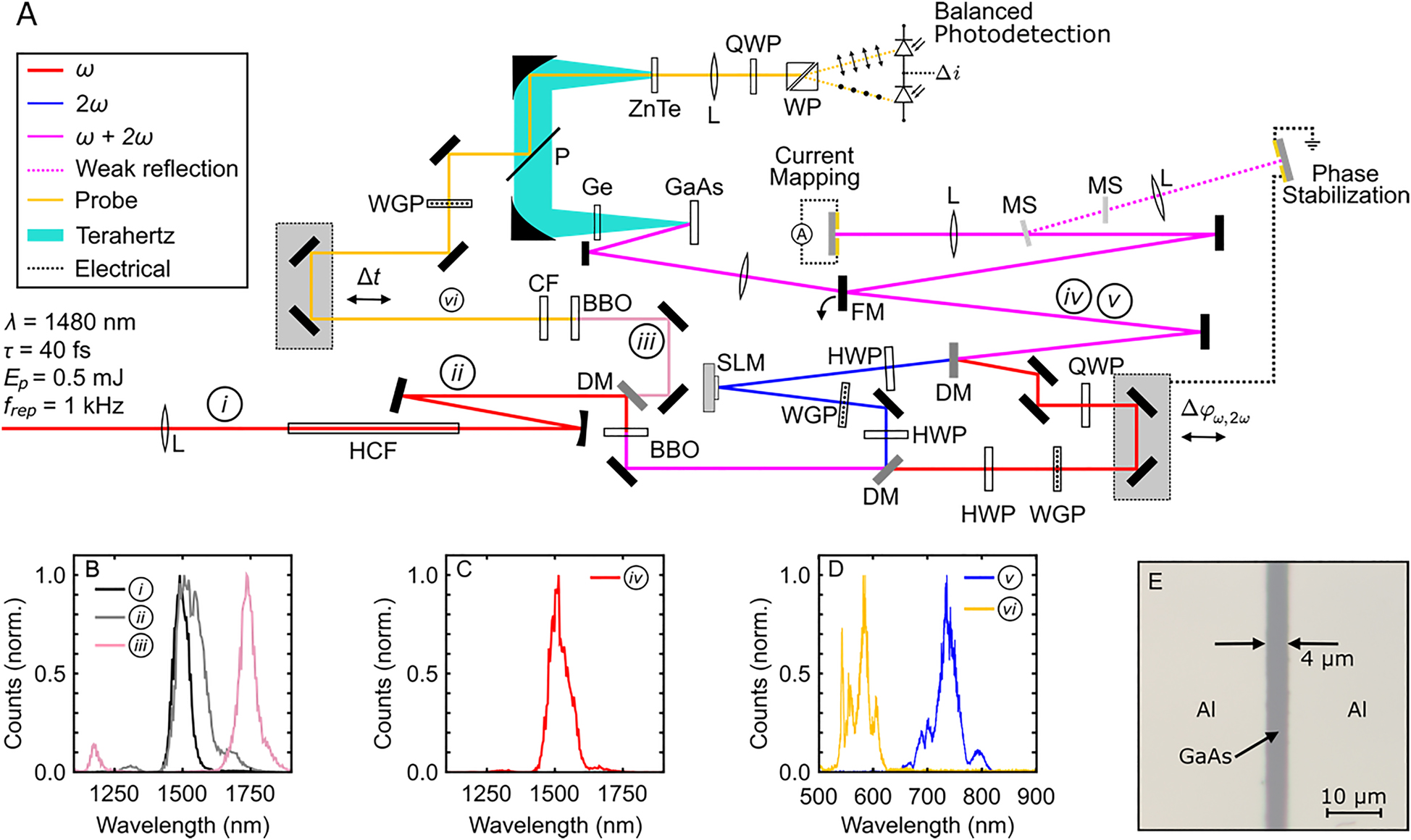
Experimental set-up. (A) The signal beam from an optical parametric amplifier (OPA) is spatially filtered and spectrally broadened using a hollow core fiber (HCF) in ambient air. A dichroic mirror (DM) transmits the spectral wings and reflects the primary spectral content. The reflected light is frequency-doubled using a
The two colors of light are diverted into separate optical paths using a DM. The energy of each beam is controlled independently using a half-wave plate and a wire grid polarizer. The
This two-color interferometer is used to coherently control currents in low temperature grown gallium arsenide (LT-GaAs). The band-gap energy
In the first measurement we use EOS to record the electric-field waveform of THz radiation emitted from LT-GaAs. When the flipper mount position is set such that the laser pulses do not reflect from the mirror, the pulses are focused onto the backside of an LT-GaAs substrate using a biconvex lens with
To generate a probe pulse that is spectrally isolated from the
In the second measurement, the flipper mount is positioned such that the
In order to detect currents excited in the LT-GaAs, we deposit two large aluminum electrodes separated by a
A weak reflection from a borosilicate microscope slide is focused onto a second LT-GaAs optoelectronic detector, which is used as a meter for
3 Results
First, we measure the THz waveform radiated from dynamic currents in GaAs. In this measurement, both the
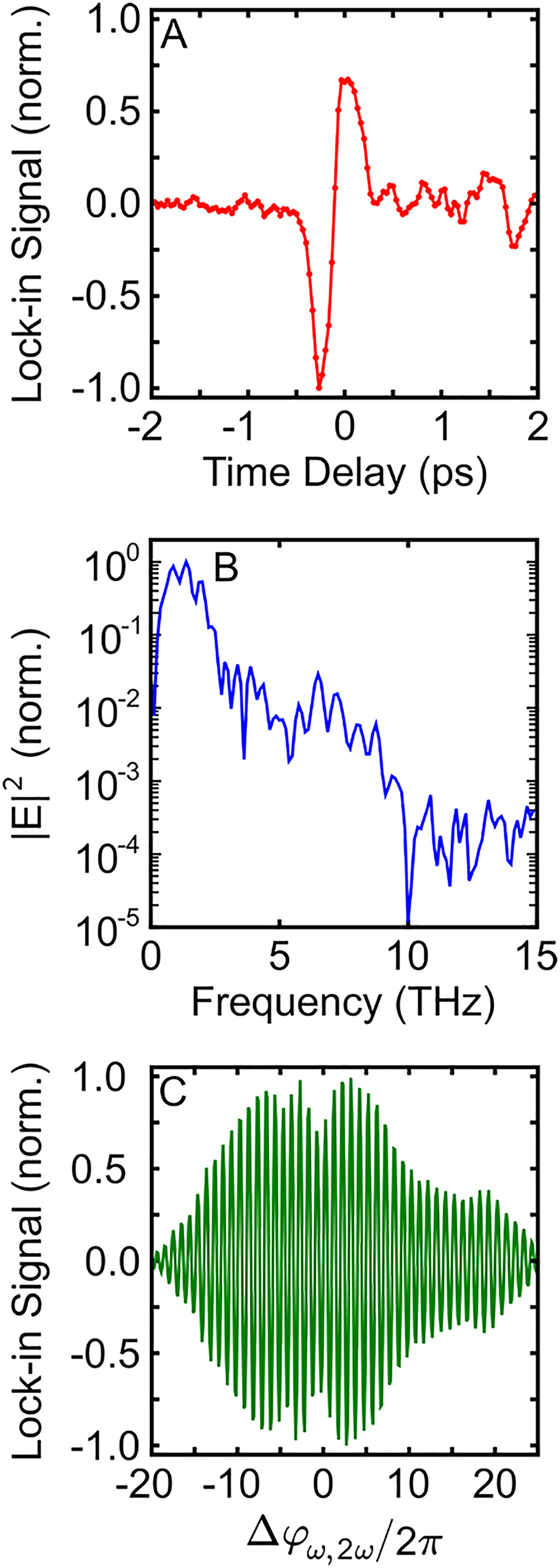
EOS of terahertz pulses. (A) Recorded electro-optic signal versus time-delay of the probe pulse. (B) Power spectral density of the waveform plotted in (A). (C) EOS signal at a fixed probe delay as
We subsequently introduce a phase pattern to the SLM for the purpose of structuring currents and THz radiation from LT-GaAs. Although, a full spatio-temporal characterization of the THz fields would provide a rigorous demonstration of the metasurface, here we focus on characterizing the source of the THz radiation, i.e., the dynamic semiconductor currents. We note that a dynamic current density acts as a source for electromagnetic radiation via the Ampère–Maxwell law:
where H is the magnetic field, J is the current density, D is the electric displacement field, and t is the time. Therefore, characterizing current density on a deeply subwavelength scale provides direct insight into the radiated THz fields.
To determine the resolution with which we can control and measure currents, we introduce a checkerboard phase pattern to the SLM (Figure 3A). The polarization of the
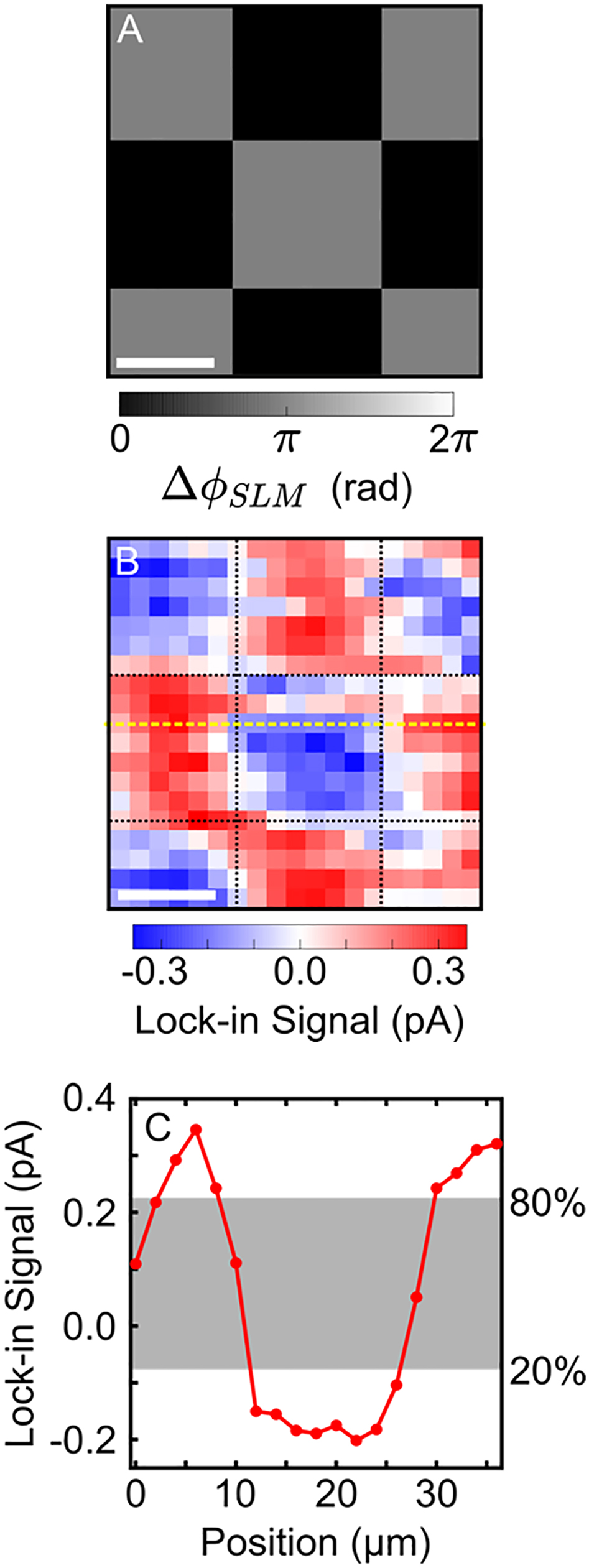
Wavelength-scale control and measurement of currents. (A) Checkerboard SLM pattern used to control micron-scale currents. The scale bar represents
A spatial mapping of the x-component of the detected current is shown in Figure 3B, where it is evident that the checkerboard pattern introduced to the SLM is transferred to the semiconductor currents. An exemplary line-out of this scan is plotted in Figure 3C, where the shaded box represents the region in which the edge between positive and negative checker squares grows from 20–80%. We use the 20–80% edge width as a measure of the combined resolution of our current control and detection schemes. By performing a statistical analysis on the entire scan shown in Figure 3B, we estimate the combined resolution to be
Next, we manipulate and measure the vectorial arrangement of the currents and demonstrate patterns that resemble metasurfaces. The split-ring resonator is a common building block for left-handed metamaterials that enables an incident electric field to excite a magnetic resonance in the structure, i.e., an oscillating ring current is excited. While a gap is required in a split-ring resonator to excite a magnetic mode, no such gap is required if the currents are generated directly. To this end, we excite a
The SLM pattern used to excite a lattice of ring currents with alternating direction is shown in Figure 4A, where a conical gradient phase structure at each lattice site controls a ring current. The application of an
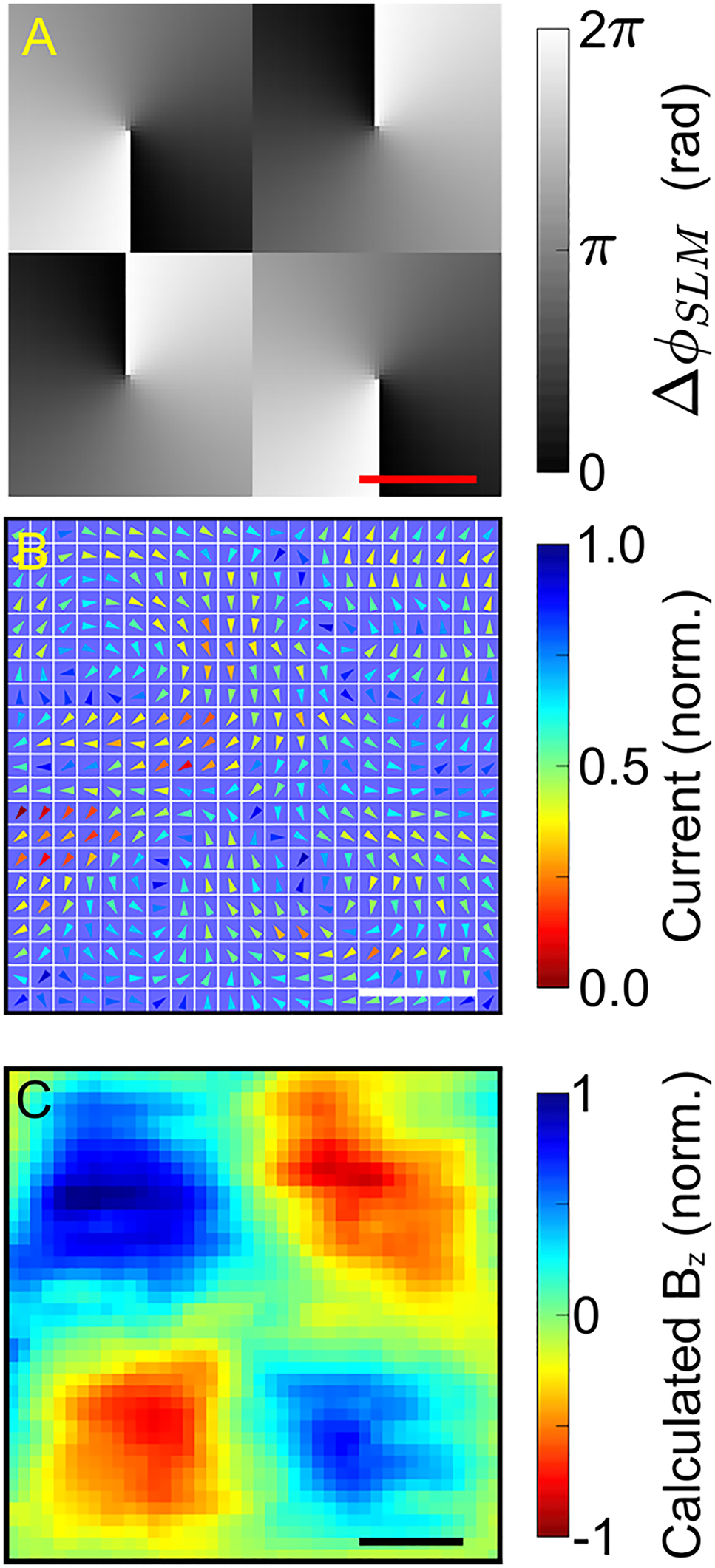
Control of magnetic field lattices. (A) The SLM pattern used to control magnetic fields. Each conical gradient controls a ring current and magnetic field at the corresponding lattice site. The scale bar represents
Assuming that the current is injected within the timescale of the laser pulse duration and relaxes with a characteristic timescale of
where
Antennas are used to transmit and receive electromagnetic signals, to generate THz radiation using photoconductive switches, to enhance and confine light–matter interaction, and as elements of metasurfaces. One common antenna design is the bowtie antenna. Using the SLM pattern in Figure 5A, we excite a dynamic bowtie antenna for THz radiation. The measured current distribution is shown in Figure 5B. The total length of this antenna is approximately
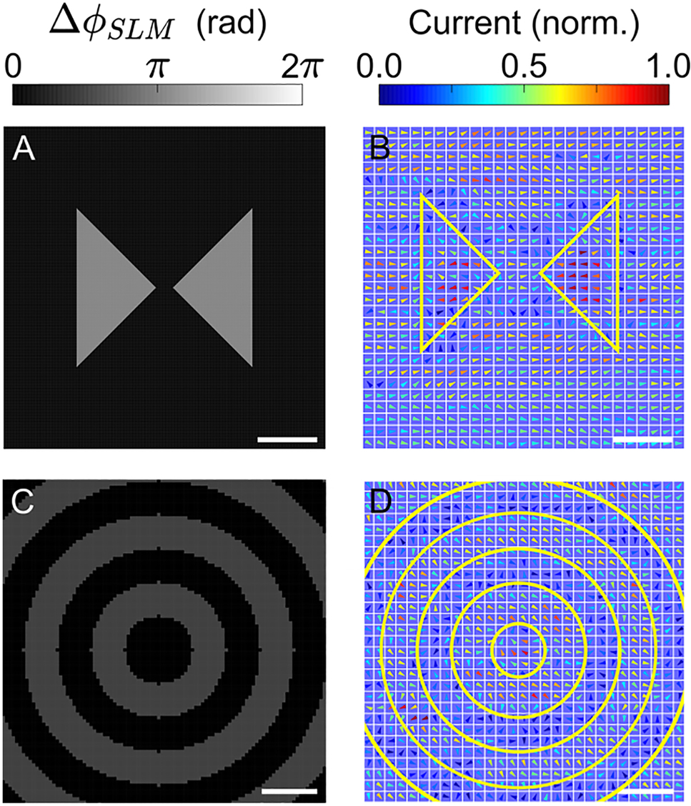
Structured currents for metasurfaces. (A) The SLM pattern used to excite a dynamic current resembling a bowtie antenna in the LT-GaAs. The scale bar represents
Although the injected currents relax within ∼100 fs, the electron-hole plasma remains for ∼1 ns. This presents the opportunity to use currents to initiate plasmons, which are subsequently sustained by the semiconductor plasma. Doing so would enable spatial structure to be imparted to surface plasmon polaritons (SPP) by the incident light. To introduce this concept, we excite a collection of concentric rings of current, or a bull’s eye structure. Bull’s eye structures have been used to achieve high transmission of light incident on the bull’s eye through a sub-diffraction aperture situated at its center, an attractive feature for near-field microscopy [47, 48]. An exemplary bull’s eye SLM pattern is shown in Figure 5C and the corresponding current measurement is plotted in Figure 5D. For this proof-of-principle, the width of each ring is kept small (approximately
4 Conclusions
Rather than sculpting light–matter interaction by introducing deeply subwavelength structures to a material, we use structured light to coherently control the spatio-vectorial arrangement of dynamic currents in LT-GaAs. By introducing one structured light beam to two-color coherent control, we have programmed and measured the current vector excited in LT-GaAs by hundreds of pixels of the two-color fields. The combined resolution of our current excitation and detection schemes is measured to be
To facilitate a reasonable data acquisition time, we have performed measurements consisting of several hundred current elements but note that most SLMs enable phase control in millions of pixels of a laser beam. Independent control of millions of current elements – each acting as a source for THz radiation – would provide similar intricacy as conventional metasurfaces. Programmable control of THz radiation introduces the possibility to apply optimization and inverse design procedures to reconfigurable metasurfaces and enables new schemes for point-to-point communications and imaging. Beyond this, it will facilitate exploration of new space-time-coupled modes of light, non-diffracting THz beams, the use of THz fields for controlling and accelerating charged particles, and THz magnetic field impulses. Finally, we note that injecting currents via strong-field coherent control could be used to increase both the spatial resolution of the currents and the frequency of the radiated fields [49, 50].
Funding source: Army Research Office
Award Identifier / Grant number: W911NF-19-1-0211
Funding source: Defense Advanced Research Projects Agency
Award Identifier / Grant number: D18AC00011
Funding source: Canada Research Chairs
Funding source: Natural Sciences and Engineering Research Council of Canada
-
Author contributions: All the authors have accepted responsibility for the entire content of this submitted manuscript and approved submission.
-
Research funding: The authors gratefully acknowledge funding from United States Defense Advanced Research Projects Agency (Topological Excitations in Electronics (TEE), agreement #D18AC00011), United States Army Research Office (award #: W911NF-19-1-0211), Natural Sciences and Engineering Research Council of Canada Discovery Grant program, Canada Research Chairs program.
-
Conflict of interest statement: The authors declare no conflicts of interest regarding this article.
References
[1] N. Yu and F. Capasso, “Flat optics with designer metasurfaces,” Nat. Mater., vol. 13, pp. 139–150, 2014. https://doi.org/10.1038/nmat3839.Search in Google Scholar PubMed
[2] W. T. Chen, A. Y. Zhu, and F. Capasso, “Flat optics with dispersion-engineered metasurfaces,” Nat. Rev. Mater., vol. 5, pp. 604–620, 2020. https://doi.org/10.1038/s41578-020-0203-3.Search in Google Scholar
[3] F. Aieta, P. Genevet, M. A. Kats, et al.., “Aberration-free ultrathin flat lenses and axicons at telecom wavelengths based on plasmonic metasurfaces,” Nano Lett., vol. 12, p. 49326, 2012. https://doi.org/10.1021/nl302516v.Search in Google Scholar PubMed
[4] A. Arbabi, Y. Horie, A. J. Ball, M. Bagheri, and A. Faraon, “Subwavelength-thick lenses with high numerical apertures and large efficiency based on high-contrast transmit arrays,” Nat. Commun., vol. 6, p. 7069, 2015. https://doi.org/10.1038/ncomms8069.Search in Google Scholar PubMed
[5] H. Zuo, D. Y. Choi, X. Gai, et al.., “High-efficiency all-dielectric metalenses for mid-infrared imaging,” Adv. Opt. Mater., vol. 5, p. 1700585, 2017. https://doi.org/10.1002/adom.201700585.Search in Google Scholar
[6] J. Engelberg, C. Zhou, N. Mazursku, J. Bar-David, A. Kristensen, and U. Levy, “Near-IR wide-field-of-view Huygens metalens for outdoor imaging applications,” Nanophotonics, vol. 9, pp. 361–370, 2019.10.1364/CLEO_QELS.2019.FTh3M.8Search in Google Scholar
[7] C. Zhang, S. Divitt, Q. Fan, et al.., “Low-loss metasurface optics down to the deep ultraviolet region,” Light Sci. Appl., vol. 9, p. 55, 2020. https://doi.org/10.1038/s41377-020-0287-y.Search in Google Scholar PubMed PubMed Central
[8] J. B. Pendry, “Negative refraction makes a perfect lens,” Phys. Rev. Lett., vol. 85, p. 3966, 2000. https://doi.org/10.1103/physrevlett.85.3966.Search in Google Scholar PubMed
[9] F. Fang, H. Lee, C. Sun, and X. Zhang, “Sub-diffraction-limited optical imaging with a silver superlens,” Science, vol. 308, pp. 534–537, 2005. https://doi.org/10.1126/science.1108759.Search in Google Scholar PubMed
[10] S. Kruk, B. Hopkins, I. I. KravchenkoII, A. Miroschnichenko, D. N. Neshev, and Y. S. Kivshar, “Invited article: broadband highly efficient dielectric metadevices for polarization control,” APL Photonics, vol. 1, p. 030801, 2016. https://doi.org/10.1063/1.4949007.Search in Google Scholar
[11] F. Ding, Z. Wang, S. He, V. M. Shalaev, and A. V. Kildishev, “Broadband high-efficiency half-wave plate: a supercell-based plasmonic metasurface approach,” ACS Nano, vol. 9, pp. 4111–4119, 2015. https://doi.org/10.1021/acsnano.5b00218.Search in Google Scholar PubMed
[12] Z. H. Jiang, L. Lin, D. Ma, et al.., “Broadband and wide field-of-view plasmonic metasurface-enabled waveplates,” Sci. Rep., vol. 4, p. 7511, 2014. https://doi.org/10.1038/srep07511.Search in Google Scholar PubMed PubMed Central
[13] Y. Yang, W. Wang, P. Moitra, I. I. KravchenkoII, D. P. Briggs, and J. Valentine, “Dielectric meta-reflect array for broadband linear polarization conversion and optical vortex generation,” Nano Lett., vol. 14, pp. 1394–1399, 2014. https://doi.org/10.1021/nl4044482.Search in Google Scholar PubMed
[14] Y. Dong, Z. Xu, N. Li, et al.., “Si metasurface half-wave plates demonstrated on a 12-inch CMOS platform,” Nanophotonics, vol. 9, pp. 149–157, 2020.10.1515/nanoph-2019-0364Search in Google Scholar
[15] M. Kang, J. Chen, X. L. Wang, and H. T. Wang, “Twisted vector field from and inhomogeneous and anisotropic metamaterial,” J. Opt. Soc. Am. B, vol. 29, pp. 572–576, 2012. https://doi.org/10.1364/josab.29.000572.Search in Google Scholar
[16] M. Kang, T. Feng, H. T. Wang, and J. Li, “Wave front engineering from an array of thin aperture antennas,” Opt Express, vol. 14, pp. 15882–15890, 2012. https://doi.org/10.1364/oe.20.015882.Search in Google Scholar
[17] H. Lingling, X. Chen, H. Mühlenbernd, et al.., “Dispersionless phase discontinuities for controlling light propagation,” Nano Lett., vol. 12, pp. 5750–5755, 2012.10.1021/nl303031jSearch in Google Scholar PubMed
[18] B. Walther, C. Helgert, C. Rockstuhl, et al.., “Spatial and spectral light shaping with metamaterials,” Adv. Mater., vol. 24, pp. 6300–6304, 2012. https://doi.org/10.1002/adma.201202540.Search in Google Scholar PubMed
[19] N. Lawrence, J. Trevino, and L. Dal Negro, “Aperiodic arrays of active nanopillars for radiation engineering,” J. Appl. Phys., vol. 111, p. 113101, 2012. https://doi.org/10.1063/1.4723564.Search in Google Scholar
[20] H. T. Chen, A. J. Taylor, and N. Yu, “A review of metasurfaces: physics and applications,” Rep. Prog. Phys., vol. 79, p. 076401, 2016. https://doi.org/10.1088/0034-4885/79/7/076401.Search in Google Scholar PubMed
[21] A. M. Shaltout, V. M. Shalaev, and M. L. Brongersma, “Spatiotemporal light control with active metasurfaces,” Science, vol. 364, p. eaat3100, 2019. https://doi.org/10.1126/science.aat3100.Search in Google Scholar PubMed
[22] H. Yang, X. Cao, F. Yang, et al.., “A programmable metasurface with dynamic polarization, scattering and focusing control,” Sci. Rep., vol. 6, p. 35692, 2016. https://doi.org/10.1038/srep35692.Search in Google Scholar PubMed PubMed Central
[23] C. Huang, C. Zhang, J. Yang, B. Sun, B. Zhao, and X. Luo, “Reconfigurable metasurface for multifunctional control of electromagnetic waves,” Adv. Opt. Mater., vol. 5, p. 1700485, 2017. https://doi.org/10.1002/adom.201700485.Search in Google Scholar
[24] R. Feng, B. Ratni, J. Yi, et al.., “Flexible manipulation of Bessel-like beams with a reconfigurable metasurface,” Adv. Opt. Mater., vol. 8, p. 2001084, 2020. https://doi.org/10.1002/adom.202001084.Search in Google Scholar
[25] R. Feng, B. Ratni, J. Yi, H. Zhang, A. De Lustrac, and S. N. Burokur, “Versatile metasurface platform for electromagnetic wave tailoring,” Photon. Res., vol. 9, pp. 1650–1659, 2021. https://doi.org/10.1364/prj.428853.Search in Google Scholar
[26] S. C. Chen, L. H. Du, K. Meng, et al.., “Terahertz wave near-field compressive imaging with a spatial resolution of over,” Opt. Lett., vol. 44, pp. 21–24, 2019. https://doi.org/10.1364/ol.44.000021.Search in Google Scholar
[27] Y. Zhang, C. Fowler, J. Liang, et al.., “Electrically reconfigurable non-volatile metasurface using low-loss optical phase-change material,” Nat. Nanotechnol., vol. 16, pp. 661–666, 2021. https://doi.org/10.1038/s41565-021-00881-9.Search in Google Scholar PubMed
[28] M. Semmlinger, M. Zhang, M. L. Tseng, et al.., “Generating third harmonic vacuum ultraviolet light with a TiO2 metasurface,” Nano Lett., vol. 19, pp. 8972–8978, 2019. https://doi.org/10.1021/acs.nanolett.9b03961.Search in Google Scholar PubMed
[29] A. Fedotova, M. Younesi, J. Sautter, et al.., “Second-harmonic generation in resonant nonlinear metasurfaces based on lithium niobate,” Nano Lett., vol. 20, pp. 8608–8614, 2020. https://doi.org/10.1021/acs.nanolett.0c03290.Search in Google Scholar PubMed
[30] M. Sivis, M. Taucer, G. Vampa, et al.., “Tailored semiconductors for high-harmonic optoelectronics,” Science, vol. 357, pp. 303–306, 2017. https://doi.org/10.1126/science.aan2395.Search in Google Scholar PubMed
[31] H. Liu, C. Guo, G. Vampa, et al.., “Enhanced high-harmonic generation from an all-dielectric metasurface,” Nat. Phys., vol. 14, pp. 1006–1010, 2018. https://doi.org/10.1038/s41567-018-0233-6.Search in Google Scholar
[32] L. Luo, I. Chatzakis, J. Wang, et al.., “Broadband terahertz generation from metamaterials,” Nat. Commun., vol. 5, p. 3055, 2014. https://doi.org/10.1038/ncomms4055.Search in Google Scholar PubMed
[33] S. Keren-Zur, M. Tal, S. Fleischer, D. M. Mittleman, and T. Ellenbogen, “Generation of spatiotemporally tailored terahertz wavepackets by nonlinear metasurfaces,” Nat. Commun., vol. 10, p. 1778, 2019. https://doi.org/10.1038/s41467-019-09811-9.Search in Google Scholar PubMed PubMed Central
[34] R. W. Hellwarth and P. Nouchi, “Focused one-cycle electromagnetic pulses,” Phys. Rev. A, vol. 54, pp. 889–895, 1996. https://doi.org/10.1103/physreve.54.889.Search in Google Scholar PubMed
[35] M. Shapiro and P. Brumer, Quantum Control of Molecular Processes, Weinheim, John Wiley & Sons, 2012.10.1002/9783527639700Search in Google Scholar
[36] E. Dupont, P. B. Corkum, H. C. Liu, M. Buchanan, and Z. R. Wasilewski, “Phase-controlled currents in semiconductors,” Phys. Rev. Lett., vol. 75, pp. 3596–3599, 1995. https://doi.org/10.1103/physrevlett.74.3596.Search in Google Scholar
[37] R. Atanasov, A. Haché, J. L. P. Hughes, H. M. van Driel, and J. E. Sipe, “Coherent control of photocurrent injection in bulk semiconductors,” Phys. Rev. Lett., vol. 76, pp. 1703–1706, 1996. https://doi.org/10.1103/physrevlett.76.1703.Search in Google Scholar
[38] A. Haché, Y. Kostoulas, R. Atanasov, J. L. P. Hughes, J. E. Sipe, and H. M. van Driel, “Observation of coherently controlled photocurrent in unbiased, bulk GaAs,” Phys. Rev. Lett., vol. 78, pp. 306–309, 1997.10.1103/PhysRevLett.78.306Search in Google Scholar
[39] A. Haché, J. E. Sipe, and H. M. van Driel, “Quantum interference control of electrical currents in GaAs,” IEEE J. Quant. Electron., vol. 34, pp. 1144–1154, 1998.10.1109/3.687857Search in Google Scholar
[40] J. M. Fraser, A. I. Shkrebtii, J. E. Sipe, and H. M. van Driel, “Quantum interference in electron-hole generation in non-centrosymmetric semiconductors,” Phys. Rev. Lett., vol. 83, pp. 4192–4195, 1999. https://doi.org/10.1103/physrevlett.83.4192.Search in Google Scholar
[41] D. Côté, J. M. Fraser, M. DeCamp, P. H. Bucksbaum, and H. M. van Driel, “THz emission from coherently controlled photocurrents in GaAs,” Appl. Phys. Lett., vol. 75, pp. 3959–3961, 1999.10.1063/1.125531Search in Google Scholar
[42] L. Costa, M. Betz, M. Spasenovic, A. D. Bristow, and H. M. van Driel, “All-optical injection of ballistic electrical currents in unbiased silicon,” Nat. Phys., vol. 3, pp. 632–635, 2007. https://doi.org/10.1038/nphys674.Search in Google Scholar
[43] M. Spasenovic, M. Betz, L. Costa, and H. M. van Driel, “All-optical injection of electrical currents in centrosymmetric semiconductors,” Phys. Rev. B, vol. 77, p. 085201, 2008.10.1103/PhysRevB.77.085201Search in Google Scholar
[44] S. Sederberg, F. Kong, and P. B. Corkum, “Tesla-scale terahertz magnetic impulses,” Phys. Rev. X, vol. 10, p. 011063, 2020. https://doi.org/10.1103/physrevx.10.011063.Search in Google Scholar
[45] S. Sederberg, F. Kong, F. Hufnagel, C. Zhang, E. Karimi, and P. B. Corkum, “Vectorized optoelectronic control and metrology in a semiconductor,” Nat. Photonics, vol. 14, pp. 680–686, 2020. https://doi.org/10.1038/s41566-020-0690-1.Search in Google Scholar
[46] K. Jana, K. R. Herperger, F. Kong, et al.., “Reconfigurable electronic circuits for magnetic fields controlled by structured light,” Nat. Photonics, vol. 15, pp. 622–626, 2021. https://doi.org/10.1038/s41566-021-00832-9.Search in Google Scholar
[47] T. Thio, K. M. Pellerin, R. A. Linke, H. J. Lezec, and T. W. Ebbesen, “Enhanced light transmission through a single subwavelength aperture,” Opt. Lett., vol. 26, pp. 1972–1974, 2001. https://doi.org/10.1364/ol.26.001972.Search in Google Scholar PubMed
[48] K. Ishihara, K. Ohashi, T. Ikari, et al.., “Terahertz-wave near-field imaging with subwavelength resolution using surface-wave-assisted bow-tie aperture,” Appl. Phys. Lett., vol. 89, p. 201120, 2006. https://doi.org/10.1063/1.2387984.Search in Google Scholar
[49] A. Schiffrin, T. Paasch-Colberg, N. Karpowicz, et al.., “Optical-field-induced current in dielectrics,” Nature, vol. 493, pp. 70–74, 2013. https://doi.org/10.1038/nature11567.Search in Google Scholar PubMed
[50] S. Sederberg, D. Zimin, S. Keiber, et al.., “Attosecond optoelectronic field measurement in solids,” Nat. Commun., vol. 11, p. 430, 2020. https://doi.org/10.1038/s41467-019-14268-x.Search in Google Scholar PubMed PubMed Central
© 2021 Kamalesh Jana et al., published by De Gruyter, Berlin/Boston
This work is licensed under the Creative Commons Attribution 4.0 International License.
Articles in the same Issue
- Frontmatter
- Editorial
- Photonic angular momentum: progress and perspectives
- Reviews
- Spiraling light: from donut modes to a Magnus effect analogy
- Orbital angular momentum and beyond in free-space optical communications
- Research Articles
- Parabolic-accelerating vector waves
- Experimental synthesis of partially coherent beam with controllable twist phase and measuring its orbital angular momentum
- Harnessing of inhomogeneously polarized Hermite–Gaussian vector beams to manage the 3D spin angular momentum density distribution
- Introducing Berry phase gradients along the optical path via propagation-dependent polarization transformations
- Angular momentum redirection phase of vector beams in a non-planar geometry
- Transverse shifts and time delays of spatiotemporal vortex pulses reflected and refracted at a planar interface
- Spatiotemporal optical vortices with arbitrary orbital angular momentum orientation by astigmatic mode converters
- Digital toolbox for vector field characterization
- Phase conjugation of twisted Gaussian Schell model beams in stimulated down-conversion
- Spin to orbital angular momentum transfer in frequency up-conversion
- Deep-learning-based recognition of multi-singularity structured light
- Reconfigurable terahertz metasurfaces coherently controlled by wavelength-scale-structured light
- Nonlinear wavefront engineering with metasurface decorated quartz crystal
- Nanostructured silica spin–orbit optics for modal vortex beam shaping
- Spin separation based on-chip optical polarimeter via inverse design
- Photonic integrated chip enabling orbital angular momentum multiplexing for quantum communication
- Fabrication of lithium niobate fork grating by laser-writing-induced selective chemical etching
- High-power thin-disk lasers emitting beams with axially-symmetric polarizations
- The generation of femtosecond optical vortex beams with megawatt powers directly from a fiber based Mamyshev oscillator
- Generation of hexagonal close-packed ring-shaped structures using an optical vortex
- A phase-to-intensity strategy of angular velocity measurement based on photonic orbital angular momentum
- SDM transmission of orbital angular momentum mode channels over a multi-ring-core fibre
- Dynamic aerosol and dynamic air-water interface curvature effects on a 2-Gbit/s free-space optical link using orbital-angular-momentum multiplexing