High-detectivity tin disulfide nanowire photodetectors with manipulation of localized ferroelectric polarization field
-
Dingshan Zheng
 ,
Hailu Wang
,
Hailu Wang
 and
Jinshui Miao
and
Jinshui Miao

Abstract
Tin sulfide semiconductor nanowires (NWs) have been widely investigated for photodetection applications because of their good optical and electrical properties. Herein, we synthesized n-type SnS2 NWs and then fabricated SnS2 NW photodetectors with a ferroelectric polymer side-gate. The strong electric field induced by ferroelectric polymer can effectively suppress the dark current and improve the detectivity in SnS2 NW photodetectors. The photodetectors after polarization depletion exhibit a high photoconductive gain of 4.0 × 10⁵ and a high responsivity of 2.1 × 10⁵ A W−1. Compared with devices without polarization depletion, the detectivity of polarization-depleted photodetectors is improved by at least two orders of magnitude, and the highest detectivity is 1.3 × 10¹⁶ Jones. Further, the rise and fall time are 56 and 91 ms respectively, which are about tens of times faster than those without polarization depletion. The device also shows a good spectral response from ultraviolet to near-infrared. This study demonstrates that ferroelectric materials can enhance optoelectronic properties of low-dimensional semiconductors for high-performance photodetectors.
1 Introduction
One-dimensional semiconductor NWs have been intensively studied for room-temperature photodetection with high sensitivity, gain and wide spectral response, etc. [1−6]. IV–VI chalcogenide tin sulfide semiconductors, including SnS [7−10] and SnS2 [11−14] shows tremendous potential in optoelectronic applications because of their narrow bandgap, high carrier mobility and light–matter coupling efficiency, etc. [9, 11]. For example, p-type SnS NWs have been synthesized and demonstrated excellent optoelectronic performance in our previous work [7]. SnS2 is an n-type semiconductor with bandgap ranging from 2.1 to 2.4 eV [11, 15], and SnS2-based nanostructures have been demonstrated to show broad prospects in field-effect transistors [14, 15], battery materials [16, 17], photodetectors [12, 13, 18], gas sensors [19], and solar cells [20, 21]. Most studies on SnS2 nanostructures mainly focus on quantum dots [22], nanosheets [12, 13, 18] and thin films [23, 24], but very limited study on SnS2 NWs. Thus, it is essential to explore 1D SnS2 NWs and their optoelectronic properties. In addition, whether it is an n-type or p-type NW photodetector, its optoelectronic performances have been greatly improved compared with traditional photodetectors. However, the large dark current is still a major problem to be solved, and it is necessary to improve these problems by designing a certain device structure or changing certain conditions of the photodetector.
In this work, we synthesized SnS2 NWs by the CVD method. To suppress the dark current caused by defect/trap induced carriers and improve the detectivity of photodetectors, we integrated ferroelectric polymer side-gate with SnS2 NW. The intrinsic carriers in the SnS2 NW channel can be depleted by ultrahigh electrostatic field induced by the polarization of ferroelectric polymer. Therefore, the background current is suppressed to as low as 10−12 A. Furthermore, the detectivity is increased by at least two orders of magnitude, and the rise and fall time are improved by tens of times. The noise characteristics show that the device has low noise equivalent power (NEP) and noise current (the frequency noise current power is ∼6.9 × 10⁻²⁸ A2 and 1/f noise current is ∼2.6 × 10⁻¹⁴ A, respectively). The SnS2 NW photodetectors after polarization depletion exhibit a high photoconductive gain of 4.0 × 10⁵, a high responsivity of 2.1 × 10⁵ A W−1 and ultra-high detectivity of 1.3 × 10¹⁶ Jones.
2 Experimental section
2.1 Nanowires synthesis and characterization
In this work, the SnS2 NWs were synthesized in a tube furnace via the CVD method. The high-purity SnS2 powder (0.1 g) was put at the heating zone center as source material and S powder (0.1 g) was put upstream of the central temperature zone to the SnS2 powder at a distance of ∼15 cm. The Au film with a thickness of 1 nm was pre-deposited onto the Si substrate as the catalyst. The substrate was put downstream approximately 12 cm away from the SnS2 powder. A carrier gas mixture of argon and hydrogen (10%) of 100 sccm was introduced into the tube. Then the temperature of the SnS2 powder was heated rapidly to 760 °C and kept at this temperature for 30 min. After that, the furnace was cooled naturally to room temperature under carrier gas flow. Scanning electron microscope (SEM), X-ray diffraction (XRD), high-resolution transmission electron microscopy (HR-TEM), and energy-dispersive X-ray spectroscopy (EDS) characterizations were performed to determine the crystal properties, diameter, elemental composition of as-synthesized SnS2 NWs together.
2.2 Photodetectors fabrication and characterization
The field-effect transistors (FETs) on the basis of single SnS2 NW can be assembled by electron-beam lithography (EBL). The SnS2 NWs were first dispersed by contact and physically transferred onto Si/SiO2 substrate with marks, following by spin-coating with MMA and PMMA. EBL with an NPGS system (JEOL 6510) was used to determine the drain and source electrodes. Before metallization, the SnS2 NWs were immersed in diluted HF (2%) solution for 15 s to eliminate the surface oxide layer. The Cr/Au (15 nm/60 nm) electrodes were completed through vacuum thermal evaporation and stripping. A ferroelectric polymer poly(vinylidene fluoride-trifluoroethylene) [P(VDF-TrFE)] with 300 nm in thickness was placed on the SnS2 NW devices through the spin-coating method. Then the P(VDF-TrFE) film was annealed at 150 °C for 3 h to enhance its crystallinity. The electrical and optoelectronic measurements of the SnS2 NW FETs were conducted with the vacuum probe station (Lake Shore TTPX) and semiconductor parameter analyzer (Keithley 4200). The time-resolved response measurements were conducted by periodically turning on and off the laser and monitored by a digital oscilloscope. Noise power spectra measurements were performed by a noise measurement system (NC300).
3 Results and discussion
The SEM image of SnS2 NWs is displayed in Figure 1a showing a uniform structure with a length of tens of micrometers and a diameter of 30–200 nm. Figure 1b shows the HR-TEM image of single SnS2 NW and the corresponding SAED pattern indicating that the SnS2 NW has a single-crystalline architecture at the [001] direction and lattice distance of 0.296 nm. The XRD (Figure 1c) and EDS (Figure 1d) characterizations also conform to the previous studies [25]. The XRD spectrum of SnS2 NWs shows all main diffraction peaks at 2θ ∼ 15.0°, 28.3°, 32.0°, 42.0°, 50.0°, 52.5°, 58.4°, corresponding to (001), (100), (101), (102), (110), (111) and (200) planes (JCPDS No. 23-0677). The EDS spectrum of the sample shows that there are elements such as C, O, Cu, Si, S and Sn, in which the presence of C and Cu is caused by the carbon micro gate substrate, while O is the oxide layer of the sample surface.
![Figure 1:
Characterizations of the as-grown SnS2 NWs. (a) SEM image of SnS2 NWs. The scale bar is 2 μm. (b) HR-TEM image indicates a single-crystalline structure along the [001] growth direction of the single SnS2 NW. The lattice distance is ∼0.296 nm and the scale bar is 2 nm. The bottom-left inset shows that the diameter of NW is about 40 nm (the scale bar is 50 nm). The top-right inset is the corresponding SAED pattern. (c) XRD pattern of the SnS2 NWs (JCPDS No. 23-0677). (d) EDS spectrum of the SnS2 NWs.](/document/doi/10.1515/nanoph-2021-0480/asset/graphic/j_nanoph-2021-0480_fig_001.jpg)
Characterizations of the as-grown SnS2 NWs. (a) SEM image of SnS2 NWs. The scale bar is 2 μm. (b) HR-TEM image indicates a single-crystalline structure along the [001] growth direction of the single SnS2 NW. The lattice distance is ∼0.296 nm and the scale bar is 2 nm. The bottom-left inset shows that the diameter of NW is about 40 nm (the scale bar is 50 nm). The top-right inset is the corresponding SAED pattern. (c) XRD pattern of the SnS2 NWs (JCPDS No. 23-0677). (d) EDS spectrum of the SnS2 NWs.
To investigate the photodetection characteristics of SnS2 NWs, back-gated SnS2 NW FETs were fabricated, as shown in Figure 2a. Figure 2b shows the I ds–V gs transfer characteristics of the device for various V ds and the linear I ds–V gs transfer characteristic at V ds = 1 V is displayed in Figure 2c. The SnS2 NW FETs exhibit typical n-type transistor behavior with a high current on-off ratio of 107 at V ds = 1 V. The electron mobility µ FE of single SnS2 NW FET is calculated using the expression: μ FE = g m L 2/(C g V ds) [26, 27], where g m = dI ds/dV gs is the transconductance and C g is the capacitance of back-gated FET. C g can be estimated on the basis of the cylinder on-plane model [26]: C g = 2πε 0 ε r L/[ln(4h/d)], where ε 0 is free space permittivity, ε r is the dielectric constant of SiO2, h = 110 nm is the thickness of the SiO2 layer, L = 3 μm is the length of the channel, d = 90 nm is the diameter of SnS2 NW (see the inset in Figure 3d). The calculated μ FE is ∼131.8 cm2 V−1 s−1 at V ds = 1 V. The electron mobility of the SnS2 NW FET is comparable with that of other n-type SnS2 nanodevices [14]. The I ds–V ds output characteristics of SnS2 FET are shown in Figure 2d. The linear I ds–V ds curves indicate good Ohmic contacts at the metal/SnS2 interface further demonstrating the n-type semiconducting behavior [13]. The net photocurrent under 520 nm illumination is 0.28 μA at a V ds = 1 V, as shown in Figure 2e. Obviously, the large dark current leads to a low I ph/I dark ratio which deteriorates the detectivity of the photodetectors.
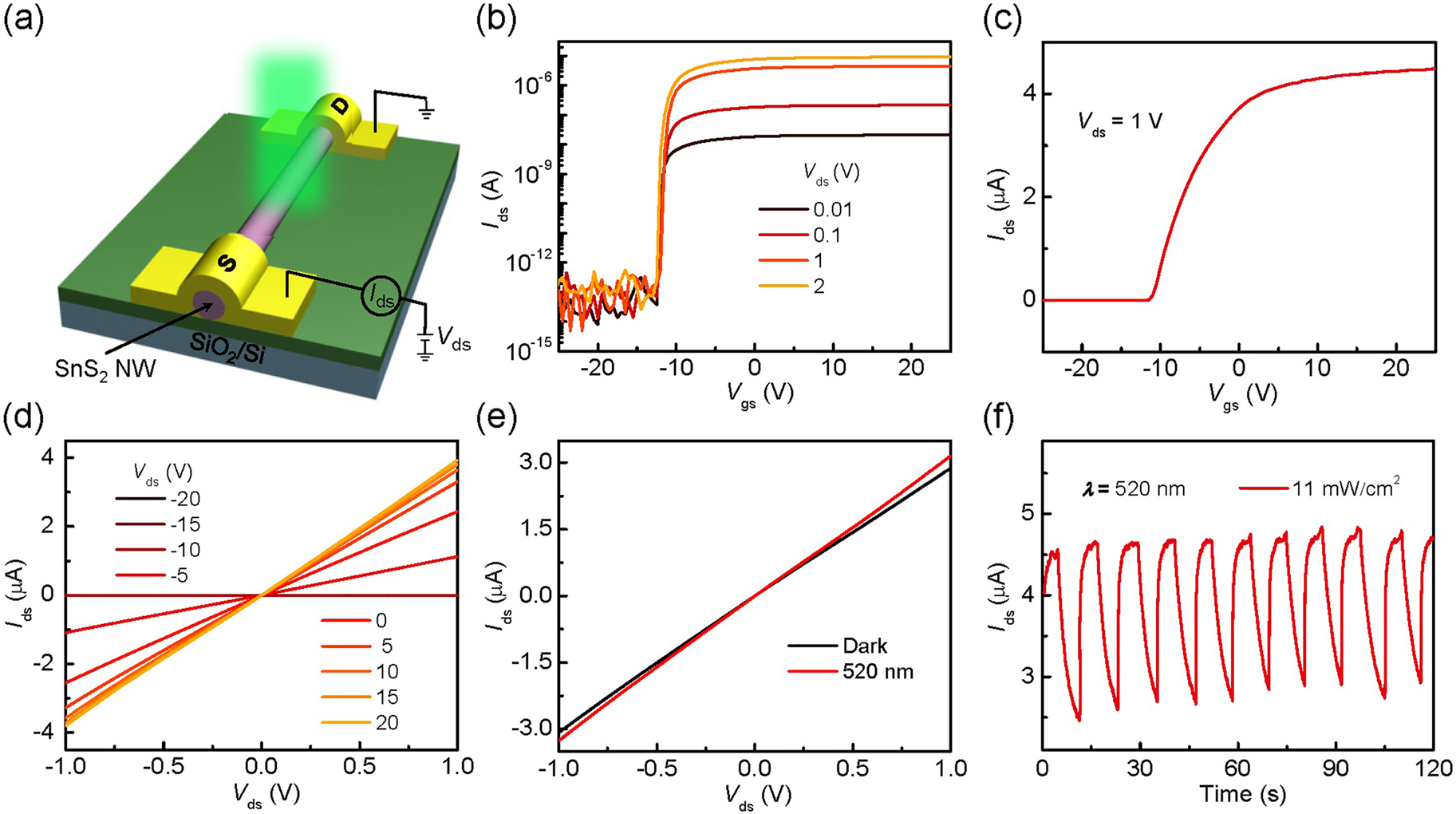
Electrical and optoelectronic properties of the single SnS2 NW back-gated FET. (a) Schematic diagram of the single SnS2 NW back-gated FET photodetector. (b) I ds–V gs transfer characteristics of the SnS2 NW FET at different bias voltages V ds. (c) Linear plot of I ds–V gs transfer characteristics at V ds = 1 V. (d) I ds–V ds output characteristics of the device, the back-gated voltage interval is 5 V. (e) I ds–V ds output characteristics of the device in dark and under the illumination of 520 nm laser, measured without additional back-gated voltage. (f) Photocurrent response of the device under optical chopping at V ds = 1 V without additional back-gated voltage (520 nm, 11 mW cm−2).
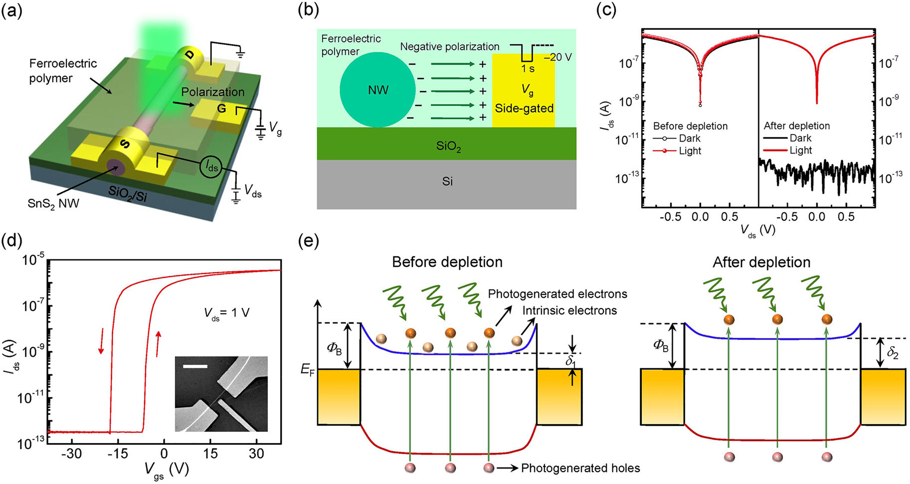
Schematic diagrams, polarization characteristics and energy band diagrams of ferroelectric side-gated single SnS2 NW photodetector. (a) Schematic illustration of ferroelectric side-gated single SnS2 NW photodetector. (b) The cross-sectional structure and schematic diagram of the device in negative polarization state. (c) Before and after being depleted by the ferroelectric polymer film, I ds–V ds characteristics of the device in the dark and upon illumination (520 nm, 11 mW cm−2). (d) I ds–V gs transfer curves of the device with local field regulation by P(VDF-TrFE) ferroelectric polymer and side-gated voltage. The inset is the SEM image of the SnS2 NW side-gated FET. (e) Energy band diagrams before and after depletion. E C is the minimum conduction band energy, E V is the maximum valence band energy, E F is the Fermi level energy, Φ B is the Schottky barrier height, and δ is the height from bottom of conduction band to the Fermi level energy. The bottom of E C rises upward and δ increases after being depleted.
The photoresponse characteristics of SnS2 NW photodetector without additional back-gated voltage (520 nm, 11 mW cm−2) are displayed in Figure 2f. Due to the surface states and crystal quality, the rise and fall time of SnS2 NW photodetectors are about 1.1 and 4.3 s [4, 28−31]. Further, the SnS2 NW photodetector exhibits a relatively low I ph/I dark ratio because of the large dark current. Therefore, to suppress the dark current we employed P(VDF-TrFE) polymer as side-gate, in which the strong local polarization field can fully deplete the carriers suppressing the dark current. The structure diagram of the device is shown in Figure 3a. The SEM image of a representative side-gated SnS2 NW device is given in the inset of Figure 3d, the distance between the NW and the side-gated electrode is 240 nm. The polarization intensity generated by ferroelectric polymer films is much higher than that of gate electrostatic field in transistors [31−36]. Figure S1 shows the hysteresis line of P(VDF-TrFE) capacitor, the coercive voltage is about 7.9 V and the remnant polarization value is about 5.2 μC cm−2, indicating the strong polarization performance of ferroelectric polymer [32]. Therefore, the stable residual polarization induced by negative voltage can largely deplete the carriers. Even the negative gate voltage is removed, the device still maintains the depletion state. Figure S2 shows the retention characteristics of the device after depletion. The device remained in the depleted state for more than 60 000 s, indicating that the device can work stably for a long time without additional negative gate voltage. Figure 3d shows the transfer properties of SnS2 NW FETs with local field regulation by P(VDF-TrFE) ferroelectric polymer dielectric and side-gated voltage. The linear curve is shown in Figure S3 in the Supplementary Materials. The hysteresis loops along the counterclockwise direction indicate that the ferroelectric local field is well regulated and has strong residual polarization characteristics [31, 32]. Noted that the dark current is suppressed to 3 × 10⁻¹³ A for side-gated voltage less than −17.2 V because of the residual polarization of the ferroelectric polymer film.
The negative polarization can deplete the intrinsic carriers in NW. For example, when a negative voltage of −20 V and pulse width of 1 s is introduced to the side-gated electrode, the ferroelectric polymer film is polarized with polarization direction from NW to the side-gated electrode. So, most free electrons in the SnS2 NW channel were depleted by the ultra-high polarization electrostatic field, as shown in Figure 3a and b. The schematic diagrams of the ferroelectric side-gated SnS2 nanowire structure before depletion and after depletion are shown in Figure S4 in the Supplementary Materials. After the electrons in the NW are depleted, the conduction band energy level rises upward, and the channel current drops below pA, in a depleted state. The energy band diagram before and after depletion is shown in Figure 3e. Because of the residual polarization in ferroelectric polymer, the dark current is largely suppressed and decreased to below 10−12 A (Figure 3c), even after removing the side-gated voltage [34]. With reduced dark current, the performance of NW photodetectors was dramatically improved. For example, the I ph/I dark ratio was improved from less than 1 to 107 and the photocurrent was also improved from 0.49 to 2.74 µA with the introduction of a strong polarization electric field. The mechanism of polarization-manipulated photodetection is shown in Figure 3e. Before depletion, the dark current comes from the thermionic emission and tunneling of the intrinsic carriers. Under illumination, the photo-generated electron–hole pairs contribute to the photocurrent together with the dark current to form the total channel current. With negative polarization, the electrons in the NW are depleted and the conduction band minimum rises upward, then the channel current under illumination is mainly attributed to the photo-generated electron–hole pairs [6, 34, 35].
Next, the photoresponse of the device with depletion was further characterized. Figure 4a shows the photo-induced I ds–V ds curves of polarization-depleted SnS2 NW photodetectors. The extracted I ph as a function of light intensity is shown in Figure 4b. The results show that the photocurrent I ph obviously depends on the light intensity (P), which can be expressed as [4] I ph = cP k , where k is 0.7 through the fitting of I ph–P curve. These results indicate complicated processes of photo-generated electron–hole generation, capture, and recombination in the SnS2 NW device [4, 7].
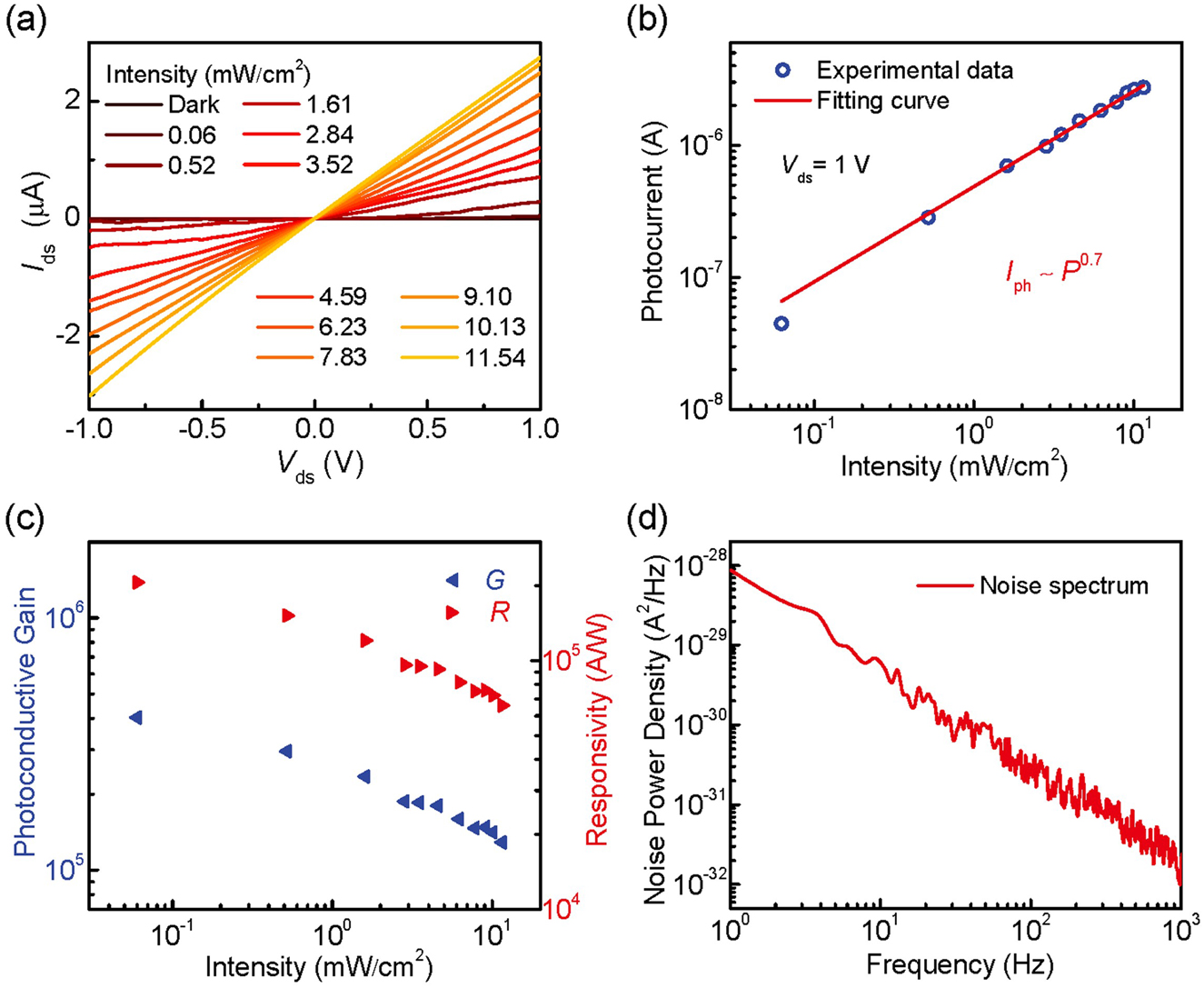
Photoresponse properties and noise power density spectra of ferroelectric side-gated single SnS2 NW photodetector. (a) I ds–V ds characteristics of the photodetector under various intensities (520 nm) after being depleted, without additional gate voltage. (b) Dependence of photocurrent on various intensities, at V ds = 1 V. (c) Dependence of photoconductive gain and responsivity on various intensities, at V ds = 1 V. (d) Noise power density spectra of the device at V ds = 1 V.
To evaluate the conversion efficiency and photoresponse of the SnS2 NW photodetector, the key parameters such as photoconductive gain (G), responsivity (R), and detectivity (D*) are characterized, and their dependence on the light intensity are also studied, as shown in Figures 4c and 5a. The photoconductive gain G of the device is defined as G = N
e/N
ph, where N
e and N
ph, respectively, represent the electron–hole pairs number and the photons number absorbed by NW in unit time [3, 31]. The G can be defined as G = (I
ph/e)/(PA/hν) [3, 31], where hν is the energy of the incident photon, e is the charge of electron, and A is the effective irradiated region of the photodetector. The effective irradiated region could be estimated through the cross-sectional area of SnS2 NW, which can be expressed as A = L × d, where L is the length of the NW channel, d is the diameter of the NW [3, 31]. The responsivity or sensitivity is also a key parameter expressing the ability of the photodetector to convert light signals into electrical signals, which can be expressed as the ratio of the output photocurrent signal of the detector to the incident light power, expressed as R = I
ph/(PA) [3, 32, 37]. Figure 4c presents the G and R of the photodetector at various light intensities and V
ds = 1 V. The results show that the G is 4.0 × 10⁵ and R is up to 2.1 × 10⁵ A W−1 under the low light intensity of 0.06 mW cm−2. Obviously, because of the high mobility of the device, the carrier transit time in the channel is short leading to high gain [3, 7]. The specific detectivity represents the minimum detectable signal of the photodetector, which is defined as D* = (AB)1/2/(NEP) [3, 38], where B and NEP represent the electrical bandwidth and the NEP. NEP is generally related to three main noise sources, namely shot noise, Johnson noise, and flicker noise (1/f noise) [34, 38]. Noise power density spectra of a single SnS2 NW photodetector was measured by a noise spectrum analyzer at 1 V bias, as shown in Figure 4d. Figure S5 shows the noise power density spectra of the device under different bias voltages. The low-frequency noise characteristics of the device at 0.1 and 1 V bias are close to the background noise at 0 V bias [34]. When the frequency is low, 1/f noise plays a dominant role, thermal noise and shot noise are independent of frequency and are not obviously observed, which is mainly because of the device’s low dark current [34, 39]. The NEP can be presented as

Detectivity, spectral and time response characterizations of ferroelectric side-gated single SnS2 NW photodetector. (a) Specific detectivity of the photodetector under various intensities, at V ds = 1 V. (b) Spectral response of the device at different illumination wavelengths from 350 to 1000 nm under light intensity of 3.8 mW cm−2, V ds = 1 V. (c) Photocurrent response of the device under optical chopping (520 nm, 11 mW cm−2) at V ds = 1 V, without additional gate voltage. (d) Time-resolved photocurrent response of the device.
Figure 5a shows that the D* is up to 1.3 × 10¹⁶ Jones at a low light intensity of 0.06 mW cm−2. Under the same conditions, D* with polarization depletion is at least two orders of magnitude higher than that of device without polarization depletion due to the reduced dark current. The SnS2 NW photodetectors with ultra-high R and D* show better performance than other photodetectors based on Tin sulfides SnS and SnS2 nanostructure reported, as shown in Table 1. Noted that the shot noise caused by dark current would be considered as the main factor restricting the device detectivity at a larger frequency range [3]. Therefore, the suppression of dark current is a critical way to improve the detectivity of the device. With ferroelectric polarization to suppress the dark current, the SnS2 NW photodetectors show an ultrahigh detectivity of 1.3 × 10¹⁶ Jones.
Comparison of the critical parameters for tin sulfides SnS and SnS2 nanostructure photodetectors.
| Photodetectors | I on/I off | Rise time | Fall time | Responsivity (A W−1) | Detectivity (Jones) | References |
|---|---|---|---|---|---|---|
| SnS NW | 1.5 | 1.2 ms | 15.1 ms | 1.6 × 10⁴ | 2.4 × 10¹² | [7] |
| SnS NB | 102 | 36 ms | 7 ms | 3 × 10² | 6 × 10⁹ | [8] |
| SnS NS | 1.3 | 5.1 ms | 8.8 ms | 156 | 2.94 × 10¹⁰ | [9] |
| SnS2 NS | 106 | 22 ms | 11 ms | 100 | [12] | |
| SnS2 NS | 103 | 5 µs | 7 µs | 8.8 × 10⁻³ | 2 × 10⁹ | [13] |
| SnS2 NS | 102 | 20 ms | 16 ms | 261 | 1.9 × 10¹⁰ | [18] |
| SnS2 NS | 2.3 | 40 ms | 80 ms | 1.1 × 10³ | 1012 | [40] |
| SnS2 NW | 107 | 56 ms | 91 ms | 2.1 × 10⁵ | 1.3 × 10¹⁶ | This work |
-
NW, nanowire; NB, nanobelt; NS, nanosheet.
The spectral response characteristics of SnS2 NW photodetector from 350 to 1000 nm are displayed in Figure 5b. Noted that the device still shows photoresponse even beyond the cut-off wavelength of 590 nm (E g ∼ 2.1 eV). The extended detection wavelength may come from the changes of surface electron–hole distribution and band structures induced by a strong ferroelectric polarization field [32, 37]. Figure S5 shows the photoresponse properties of ferroelectric side-gated SnS2 NW photodetector after depletion under deep ultraviolet illumination (280 nm). The device exhibits ultra-sensitive photoresponse and wider spectrum detection from ultraviolet to near-infrared [32, 36]. The time-resolved photoresponse was conducted under 520 nm illumination, shown in Figure 5c. The SnS2 NW device exhibits good switching periodicity and stability, and the I light/I dark ratio is as high as 107. To precisely measure the device’s rise and fall times, a digital oscilloscope was applied to monitor fast-changing photocurrent signals [41, 42]. Figure 5d shows the time-resolution photocurrent response, and the rise time and fall time are 56 and 91 ms respectively. The rise and fall time are tens of times faster than those without ferroelectric polarization. The faster response and recovery time exhibit the faster generation and recombination of electron–hole pairs, which may be related to ultra-high ferroelectric polarization local field generated by P(VDF-TrFE) ferroelectric polymer [30, 34, 43].
4 Conclusions
In this work, we demonstrated CVD-grown SnS2 NWs for photodetectors. To reduce the dark current, the ferroelectric side-gate was integrated with SnS2 NW photodetectors. The dark current is significantly suppressed and minimized after depletion through the ultra-high electrostatic polarization, even after removing the side-gated voltage. The ferroelectric side-gated devices show a large photoconductive gain, ultra-high detectivity and responsivity, rapid response speed, and good spectral response characteristics from ultraviolet to near-infrared. This work opens new avenues for ferroelectric-manipulated photodetection technology.
Funding source: Science Foundation of Educational Commission of Hubei Province of China
Award Identifier / Grant number: T2020008
Funding source: Natural Science Foundation of Hubei Province of China
Award Identifier / Grant number: 2018CFB567
Funding source: National Natural Science Foundation of China
Award Identifier / Grant number: 11774054, 12075036, 11947077, 62005303
Funding source: Hubei Education Department Science and Technology Research Project
Award Identifier / Grant number: B2019040
-
Author contribution: All the authors have accepted responsibility for the entire content of this submitted manuscript and approved submission.
-
Research funding: The research was supported by the National Natural Science Foundation of China (Grant No. 11774054, 12075036, 11947077, 62005303), Science Foundation of Educational Commission of Hubei Province of China (Grant No. T2020008), Natural Science Foundation of Hubei Province of China (Grant No. 2018CFB567) and Hubei Education Department Science and Technology Research Project (Grant No. B2019040).
-
Conflict of interest statement: The authors declare no conflicts of interest.
References
[1] X. F. Duan, Y. Huang, Y. Cui, et al.., “Indium phosphide nanowires as building blocks for nanoscale electronic and optoelectronic devices,” Nature, vol. 409, pp. 66–69, 2001. https://doi.org/10.1038/35051047.Search in Google Scholar PubMed
[2] J. Zhu, Z. F. Yu, G. F. Burkhard, et al.., “Optical absorption enhancement in amorphous silicon nanowire and nanocone arrays,” Nano Lett., vol. 9, pp. 279–282, 2009. https://doi.org/10.1021/nl802886y.Search in Google Scholar PubMed
[3] X. Liu, L. L. Gu, Q. P. Zhang, et al.., “All-printable band-edge modulated ZnO nanowire photodetectors with ultra-high detectivity,” Nat. Commun., vol. 9, p. 4007, 2014. https://doi.org/10.1038/ncomms5007.Search in Google Scholar PubMed PubMed Central
[4] N. Guo, W. D. Hu, L. Liao, et al.., “Anomalous and highly efficient InAs nanowire phototransistors based on majority carrier transport at room temperature,” Adv. Mater., vol. 26, pp. 8203–8209, 2014. https://doi.org/10.1002/adma.201403664.Search in Google Scholar PubMed
[5] M. Luo, F. Ren, N. Gagrani, et al.., “Polarization-independent indium phosphide nanowire photodetectors,” Adv. Opt. Mater., vol. 8, p. 2000514, 2020. https://doi.org/10.1002/adom.202000514.Search in Google Scholar
[6] Z. H. Wang and B. Nabet, “Nanowire optoelectronics,” Nanophotonics, vol. 4, pp. 491–502, 2015. https://doi.org/10.1515/nanoph-2015-0025.Search in Google Scholar
[7] D. S. Zheng, H. H. Fang, M. S. Long, et al.., “High-performance near-infrared photodetectors based on p-type SnX (X= S, Se) nanowires grown via chemical vapor deposition,” ACS Nano, vol. 12, pp. 7239–7245, 2018. https://doi.org/10.1021/acsnano.8b03291.Search in Google Scholar PubMed
[8] X. Zhou, L. Gan, Q. Zhang, et al.., “High performance near-infrared photodetectors based on ultrathin SnS nanobelts grown via physical vapor deposition,” J. Mater. Chem. C, vol. 4, pp. 2111–2116, 2016. https://doi.org/10.1039/c5tc04410c.Search in Google Scholar
[9] G. Z. Liu, Y. Li, B. Li, et al.., “High-performance photodetector based on two-dimensional Tin (II) sulfide (SnS) nanoflakes,” J. Mater. Chem. C, vol. 6, pp. 10036–10041, 2018. https://doi.org/10.1039/c8tc03501f.Search in Google Scholar
[10] L. Wu, Z. Xie, L. Lu, et al.., “Few-layer tin sulfide: a promising black-phosphorus-analogue 2D material with exceptionally large nonlinear optical response, high stability, and applications in all-optical switching and wavelength conversion,” Adv. Opt. Mater., vol. 6, p. 1700985, 2018. https://doi.org/10.1002/adom.201700985.Search in Google Scholar
[11] Y. J. Gong, H. T. Yuan, C. L. Wu, et al.., “Spatially controlled doping of two-dimensional SnS2 through intercalation for electronics,” Nat. Nanotechnol., vol. 13, pp. 294–299, 2018. https://doi.org/10.1038/s41565-018-0069-3.Search in Google Scholar PubMed
[12] Y. Huang, H. X. Deng, K. Xu, et al.., “Highly sensitive and fast phototransistor based on large size CVD-grown SnS2 nanosheets,” Nanoscale, vol. 7, pp. 14093–14099, 2015. https://doi.org/10.1039/c5nr04174k.Search in Google Scholar PubMed
[13] G. X. Su, V. G. Hadjiev, P. E. Loya, et al.., “Chemical vapor deposition of thin crystals of layered semiconductor SnS2 for fast photodetection application,” Nano Lett., vol. 15, pp. 506–513, 2015. https://doi.org/10.1021/nl503857r.Search in Google Scholar PubMed
[14] H. S. Song, S. L. Li, L. Gao, et al.., “High-performance top-gated monolayer SnS2 field-effect transistors and their integrated logic circuits,” Nanoscale, vol. 5, pp. 9666–9670, 2013. https://doi.org/10.1039/c3nr01899g.Search in Google Scholar PubMed
[15] D. De, J. Manongdo, S. See, et al.., “High on/off ratio field effect transistors based on exfoliated crystalline SnS2 nano-membranes,” Nanotechnology, vol. 24, p. 025202, 2013. https://doi.org/10.1088/0957-4484/24/2/025202.Search in Google Scholar PubMed
[16] M. S. Balogun, W. T. Qiu, J. H. Jian, et al.., “Vanadium nitride nanowire supported SnS2 nanosheets with high reversible capacity as anode material for lithium ion batteries,” ACS Appl. Mater. Interfaces, vol. 7, pp. 23205–23215, 2015. https://doi.org/10.1021/acsami.5b07044.Search in Google Scholar PubMed
[17] H. Y. Sun, M. Ahmad, J. Luo, et al.., “SnS2 nanoflakes decorated multiwalled carbon nanotubes as high performance anode materials for lithium-ion batteries,” Mater. Res. Bull., vol. 49, pp. 319–324, 2014. https://doi.org/10.1016/j.materresbull.2013.09.005.Search in Google Scholar
[18] X. Zhou, Q. Zhang, L. Gan, et al.., “Large-size growth of ultrathin SnS2 nanosheets and high performance for phototransistors,” Adv. Funct. Mater., vol. 26, pp. 4405–4413, 2016. https://doi.org/10.1002/adfm.201600318.Search in Google Scholar
[19] W. J. Yan, C. Z. Lv, D. Zhang, et al.., “Enhanced NO2 sensitivity in Schottky contacted n-type SnS2 gas sensors,” ACS Appl. Mater. Interfaces, vol. 12, pp. 26746–26754, 2020. https://doi.org/10.1021/acsami.0c07193.Search in Google Scholar PubMed
[20] X. D. Cui, W. W. Xu, Z. Q. Xie, et al.., “High-performance dye-sensitized solar cells based on Ag-doped SnS2 counter electrode,” J. Mater. Chem. A, vol. 4, pp. 1908–1914, 2016. https://doi.org/10.1039/c5ta10234k.Search in Google Scholar
[21] X. Chen, Y. Hou, B. Zhang, et al.., “Low-cost SnSx counter electrodes for dye-sensitized solar cells,” Chem. Commun., vol. 49, pp. 5793–5795, 2013. https://doi.org/10.1039/c3cc42679c.Search in Google Scholar PubMed
[22] Y. F. Huang, W. C. Jiao, Z. M. Chu, et al.., “SnS2 quantum dot-based optoelectronic flexible sensors for ultrasensitive detection of NO2 down to 1 ppb,” ACS Appl. Mater. Interfaces, vol. 12, pp. 25178–25188, 2020. https://doi.org/10.1021/acsami.0c05240.Search in Google Scholar PubMed
[23] A. J. Khimani, S. H. Chaki, S. M. Chauhan, et al.., “Influence of deposition techniques on quality and photodetection properties of tin disulfide (SnS2) thin films,” J. Mater. Sci. Mater. Electron., vol. 30, pp. 13118–13133, 2019. https://doi.org/10.1007/s10854-019-01675-5.Search in Google Scholar
[24] S. K. Panda, A. Antonakos, E. Liarokapis, et al.., “Optical properties of nanocrystalline SnS2 thin films,” Mater. Res. Bull., vol. 42, pp. 576–583, 2007. https://doi.org/10.1016/j.materresbull.2006.06.028.Search in Google Scholar
[25] M. Zervos, C. N. Mihailescu, J. Giapintzakis, et al.., “Surface passivation and conversion of SnO2 to SnS2 nanowires,” Mater. Sci. Eng. B, vol. 198, pp. 10–13, 2015. https://doi.org/10.1016/j.mseb.2015.03.006.Search in Google Scholar
[26] X. M. Zou, X. Q. Liu, C. L. Wang, et al.., “Controllable electrical properties of metal-doped In2O3 nanowires for high-performance enhancement mode transistors,” ACS Nano, vol. 7, pp. 804–810, 2013. https://doi.org/10.1021/nn305289w.Search in Google Scholar PubMed
[27] J. S. Miao, W. D. Hu, N. Guo, et al.., “Single InAs nanowire room-temperature near-infrared photodetectors,” ACS Nano, vol. 8, pp. 3628–3635, 2014. https://doi.org/10.1021/nn500201g.Search in Google Scholar PubMed
[28] S. Jeon, S. E. Ahn, I. Song, et al.., “Gated three-terminal device architecture to eliminate persistent photoconductivity in oxide semiconductor photosensor arrays,” Nat. Mater., vol. 11, pp. 301–305, 2012. https://doi.org/10.1038/nmat3256.Search in Google Scholar PubMed
[29] W. J. Luo, Q. C. Weng, M. S. Long, et al.., “Room-temperature single-photon detector based on single nanowire,” Nano Lett., vol. 18, pp. 5439–5445, 2018. https://doi.org/10.1021/acs.nanolett.8b01795.Search in Google Scholar PubMed
[30] H. L. Wang, F. Wang, H. Xia, et al., “Direct observation and manipulation of hot electrons at room temperature,” Natl. Sci. Rev., vol. 8, p. nwaa295, 2021. https://doi.org/10.1093/nsr/nwaa295.Search in Google Scholar PubMed PubMed Central
[31] D. S. Zheng, J. L. Wang, W. D. Hu, et al.., “When nanowires meet ultrahigh ferroelectric field-high-performance full-depleted nanowire photodetectors,” Nano Lett., vol. 16, pp. 2548–2555, 2016. https://doi.org/10.1021/acs.nanolett.6b00104.Search in Google Scholar PubMed
[32] X. D. Wang, P. Wang, J. L. Wang, et al.., “Ultrasensitive and broadband MoS2 photodetector driven by ferroelectrics,” Adv. Mater., vol. 27, pp. 6575–6581, 2015. https://doi.org/10.1002/adma.201503340.Search in Google Scholar PubMed
[33] M. Su, Z. Y. Yang, L. Liao, et al.., “Side-gated In2O3 nanowire ferroelectric FETs for high-performance nonvolatile memory applications,” Adv. Sci., vol. 3, p. 1600078, 2016. https://doi.org/10.1002/advs.201600078.Search in Google Scholar PubMed PubMed Central
[34] D. S. Zheng, H. H. Fang, P. Wang, et al.., “High-performance ferroelectric polymer side-gated CdS nanowire ultraviolet photodetectors,” Adv. Funct. Mater., vol. 26, pp. 7690–7696, 2016. https://doi.org/10.1002/adfm.201603152.Search in Google Scholar
[35] H. H. Fang and W. D. Hu, “Photogating in low dimensional photodetectors,” Adv. Sci., vol. 4, p. 1700323, 2017. https://doi.org/10.1002/advs.201700323.Search in Google Scholar PubMed PubMed Central
[36] X. T. Zhang, H. Huang, X. M. Yao, et al.., “Ultrasensitive mid-wavelength infrared photodetection based on a single InAs nanowire,” ACS Nano, vol. 13, pp. 3492–3499, 2019. https://doi.org/10.1021/acsnano.8b09649.Search in Google Scholar PubMed
[37] X. Gong, M. H. Tong, Y. J. Xia, et al.., “High-detectivity polymer photodetectors with spectral response from 300 nm to 1450 nm,” Science, vol. 325, pp. 1665–1667, 2009. https://doi.org/10.1126/science.1176706.Search in Google Scholar PubMed
[38] J. R. Manders, T.-H. Lai, Y. B. An, et al.., “Low-noise multispectral photodetectors made from all solution-processed inorganic semiconductors,” Adv. Funct. Mater., vol. 24, pp. 7205–7210, 2014. https://doi.org/10.1002/adfm.201402094.Search in Google Scholar
[39] S. P. Chang, C. Y. Lu, S. J. Chang, et al.., “Electrical and optical characteristics of UV photodetector with interlaced ZnO nanowires,” IEEE J. Sel. Top. Quant. Electron., vol. 17, pp. 990–995, 2011. https://doi.org/10.1109/jstqe.2010.2046884.Search in Google Scholar
[40] Y. Fu, G. Y. Gou, X. W. Wang, et al.., “High-performance photodetectors based on CVD-grown high-quality SnS2 nanosheets,” Appl. Phys. A, vol. 123, p. 299, 2017. https://doi.org/10.1007/s00339-017-0883-8.Search in Google Scholar
[41] H. H. Fang, W. D. Hu, P. Wang, et al.., “Visible light-assisted high-performance mid-infrared photodetectors based on single InAs nanowire,” Nano Lett., vol. 16, pp. 6416–6424, 2016. https://doi.org/10.1021/acs.nanolett.6b02860.Search in Google Scholar PubMed
[42] P. Wang, S. S. Liu, W. J. Luo, et al.., “Arrayed van der waals broadband detectors for dual-band detection,” Adv. Mater., vol. 29, p. 1604439, 2017. https://doi.org/10.1002/adma.201604439.Search in Google Scholar PubMed
[43] L. Y. Zhang, X. Q. Xiu, Y. W. Li, et al.., “Solar-blind ultraviolet photodetector based on vertically aligned single-crystalline β-Ga2O3 nanowire arrays,” Nanophotonics, vol. 9, pp. 4497–4503, 2020. https://doi.org/10.1515/nanoph-2020-0295.Search in Google Scholar
Supplementary Material
The online version of this article offers supplementary material (https://doi.org/10.1515/nanoph-2021-0480).
© 2021 Dingshan Zheng et al., published by De Gruyter, Berlin/Boston
This work is licensed under the Creative Commons Attribution 4.0 International License.
Articles in the same Issue
- Frontmatter
- Review
- Examples in the detection of heavy metal ions based on surface-enhanced Raman scattering spectroscopy
- Scalable and effective multi-level entangled photon states: a promising tool to boost quantum technologies
- Research Articles
- Observation of intensity flattened phase shifting enabled by unidirectional guided resonance
- Plasmonic nanocrystals on polycarbonate substrates for direct and label-free biodetection of Interleukin-6 in bioengineered 3D skeletal muscles
- Experimental demonstration of cylindrical vector spatiotemporal optical vortex
- Establishing exhaustive metasurface robustness against fabrication uncertainties through deep learning
- Investigation of dipole emission near a dielectric metasurface using a dual-tip scanning near-field optical microscope
- Multi-class, multi-functional design of photonic topological insulators by rational symmetry-indicators engineering
- Inverse design of organic light-emitting diode structure based on deep neural networks
- A wavelength and polarization selective photon sieve for holographic applications
- Direct-access mode-division multiplexing switch for scalable on-chip multi-mode networks
- Toward spectrometerless instant Raman identification with tailored metasurfaces-powered guided-mode resonances (GMR) filters
- Long-range qubit entanglement via rolled-up zero-index waveguide
- Pump-controlled RGB single-mode polymer lasers based on a hybrid 2D–3D μ-cavity for temperature sensing
- Unidirectional emission of phase-controlled second harmonic generation from a plasmonic nanoantenna
- Self-assembled multifunctional nanostructures for surface passivation and photon management in silicon photovoltaics
- Stoichiometric modulation on optical nonlinearity of 2D MoS x Se2−x alloys for photonic applications
- High-detectivity tin disulfide nanowire photodetectors with manipulation of localized ferroelectric polarization field