Observation of intensity flattened phase shifting enabled by unidirectional guided resonance
-
Zixuan Zhang


Abstract
Phase-only light modulation is an important functionality for many optoelectronic applications. Although modulation efficiency can be significantly improved by using optical resonances, resonance detuning is always accompanied with dramatic intensity variation that is less ideal. Here, we propose a method to achieve intensity-flattened phase shifting by utilizing the unidirectional guided resonance (UGR) – a novel class of topologically enabled guided resonance that only radiates toward a single side. Consequently, the incident excites resonances and generates phase shifting, but it transmits to only one out-going port without other choice, which flattens the transmittance. Theory and simulation agree well and confirm our findings, in particular when nonradiative loss has been taken into account. By directly measuring the intensity and phase responses of UGR samples, a dip depth of 0.43 is observed with nonradiative Q around 2500. We further predict a dip depth of 0.13 can be achieved with a reasonable nonradiative Q around 8000 in state-of-art fabrication precision, which is sufficient and useful for the applications ranging from light projection, flat metalens optics, optical phased array, to light detection and ranging.
1 Introduction
Phase shifting is an important functionality for a variety of optoelectronic applications. Examples range from phase modulators for optical communication [1–3], interferometry [4, 5], wave-front manipulation of metasurfaces [6–8] and beam steering of optical phased arrays [9–11]. Since phase accumulation relies on both the change of refractive index and structural geometry, various phase shifters are built from thermal-optically [12–14] or electro-optically [15–17] modifying refractive index, or alternatively, changing optical path in static [6, 18] or dynamic manners [10, 19]. However, achieving phase shifting in chip scale suffers from the insufficient efficiency in modifying refractive index, and limited footprint to change the light path. To overcome such shortcomings, optical resonances are usually applied [5, 20], [21], [22], [23], [24].
Optical resonances capture, trap the incident light, and release it in a period of photon lifetime. During this process, the phase of light dramatically changes according to the quality factor Q of resonances in a modal volume V [25]. By promoting the Q and shrinking the V [26], phase shifters are expected to be more efficient and compact. However, while resonance brings strong phase shifting, it is also accompanied with dramatic modification in intensity response at the same time [27], which makes it less ideal for many application scenarios. Therefore, it is theoretically interesting and practically important to find out whether it is possible to realize phase shifting alone with flattened intensity varying, when optical resonances are introduced.
Here, we theoretically propose that nearly perfect intensity-invariant phase shifting can be achieved by utilizing a novel class of topologically enabled unidirectional guided resonances (UGRs) [28] in a photonic crystal (PhC) slab, and experimentally observe in realistic samples that the intensity varying is indeed dramatically flattened during the phase shifting. UGRs are unique since they only radiate toward a single side of PhC slab while completely forbid the radiation on the other side. This phenomenon origins from the consequence of topological charge evolution – the winding number of topological defects [29] in polarization vector field characterizing the radiation [30–35]. Specifically, integer topological charges correspond to a complete elimination of light escaping, known as the bound states in the continuum (BIC) [36, 37]. By breaking structural symmetries, an integer topological charge splits into two half-integer charges, carried by two circular polarized (CP) states in opposite helicities [38]. Through tuning structure parameters, the half-charges combine and restore as an integer charge at a single-side of PhC but remain separated at the other side, consequently, creating UGRs. Theory and experiment have confirmed the existence and effectiveness of UGRs [28].
The principle of the intensity flattened phase shifting relies on the UGRs for closing extra radiation channels. When an incident light goes through the PhC slab, part of the light transmit and reflect directly, while the other part couples into the resonance and radiates out. Unlike conventional guided resonances that radiate toward both upper and lower sides, the UGRs only radiate to one single side, which implies that all the light coupled into the UGR would eventually return to the same channel, resulting in phase shifting with unchanged intensity. This feature separates the intensity and phase responses of a single resonance, which would be particularly useful for manipulating wave-fronts in a flexible way to realize flat metalens, programmable metasurfaces, and large-scale optical phase arrays.
2 Principle and theory
We start by considering an arbitrary guided resonance embedded in a uniform medium whose in-plane momentum is specified as k. In general, the interaction between incident light and resonance can be depicted by a 4-port model of temporal coupled mode theory (TCMT) [39], as illustrated in Figure 1a. Assuming a plane-wave incident with in-plane momentum k inputs from Port 3 (left-plane), a part of the incident doesn’t interact with the resonance but directly passes through to Port 2 or reflects to Port 4 (mid-plane), while the other part excites the resonance under phase-matching condition, which radiates toward Port 2 and 4, respectively (right-plane). Therefore, observed from Port 2 and 4, the transmittance and reflectance depend on how much incident energy coupled to the resonance, which can be quite different under on- or off-resonance excitation.
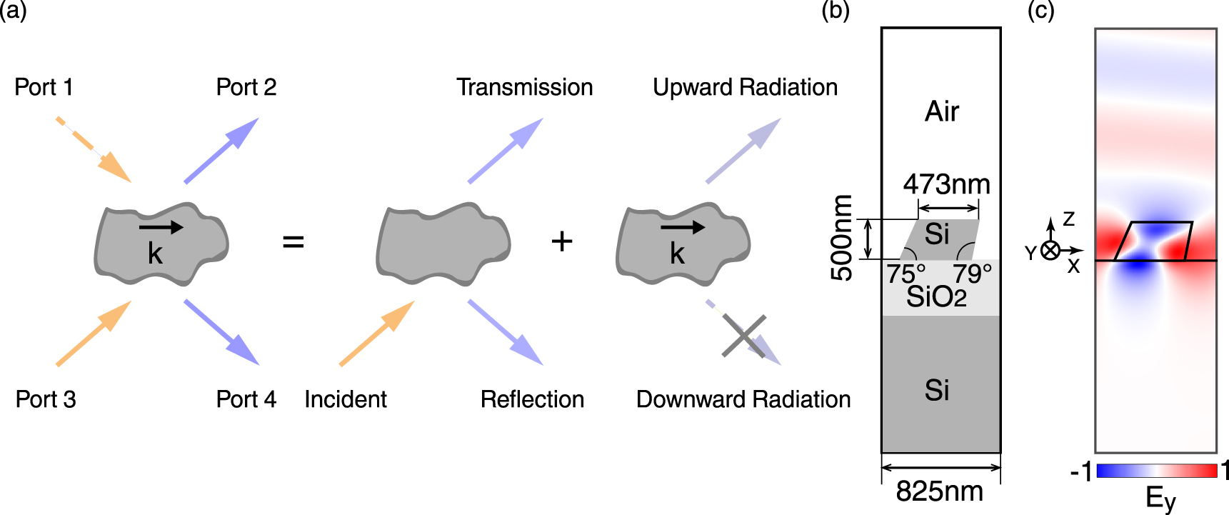
Theory of guided resonance excitation and radiation.
(a) A schematic for the four-port TCMT model. Left panel: the guided resonance with in-plane momentum k couples to the outside with four channels. Middle panel: part of the incident from Port 3 reflects and transmits directly without interacting with the resonance. Right panel: the resonance radiates toward the upper and lower sides, while the downward radiation is forbidden by the UGR. (b) The cross-section of unit-cell for a UGR design on SOI wafer. (c) The E y field pattern of UGR in a unit-cell calculated from numerical simulation.
Such a process can be modeled by using TCMT [40]. Here, we assume weak coupling, linearity, energy conservation, and time-reversal symmetry in the system. Although the incident wave only couples to resonance and out-going waves with the same k (conservation of Bloch momentum), to describe time-reversal symmetry constraints for general geometries and incident angles, we need to include the resonance at −k as well, resulting in a two-resonance, four-port model:
in which:
Here, A 1,2 are the amplitudes of resonances at k and −k, but their center frequencies are necessarily identical due to the law of reciprocity, then we denote it as ω 0; τ and τ nr represent the radiative and nonradiative lifetime of resonance, respectively. S ± are the amplitudes of the input and out-going waves; K and D are the coupling matrices that depict the strength of coupling into and out of the resonance, using subscripts (i = 1, 2, 3, 4) to denote the 4 ports as shown in Figure 1a; C is the scattering matrix for the direct (nonresonant) transmission and reflection through the resonance.
Since time-reversal flips the two resonances at k
±, we have d
i
= κ
i
. By imposing the constraint of energy-conservation, we got
Furthermore, we assume the guided resonance is a UGR at in-plane momentum of k, namely the resonance only radiates toward Port 2 while Port 4 is closed. A realistic design is presented in Figure 1b and c, as we elaborated in our previous work [28]. Briefly, the structure consists of a series of equally spaced one-dimensional bars in a period of 825 nm, fabricated on a silicon-on-insulator (SOI) wafer with a silicon layer of 500 nm and silica box layer of 2 μm. The silicon bar is trapezoidal in general, showing that the structure possess no symmetry in 180° rotation (C 2) or up–down mirror (σ z ). The upper surface of the trapezoid is 473 nm and the two side-walls are in angles of 75° and 79°, respectively. The modal pattern of E y field at resonance wavelength of 1551 nm is illustrated in Figure 1c, confirming the UGR is singled-sided radiative. The quality factor Q r of the UGR is 277.
At UGRs, we have d
4 = 0. Together with the relations of
Therefore, S 34 and S 32 can also be simplified as:
As a result, under the limit that nonradiative loss is negligible, i.e., τ nr → ∞, we derive that the reflectance and transmittance become:
From Eqs. (9) and (10), we find that the reflectance and transmittance upon UGR are pinned to the background reflection and transmission, and don’t exhibit any features of the resonance. Namely from the intensity measurement, the resonance becomes invisible, which is quite different from conventional observation of guided resonances. We confirm this finding from numerical simulations by using the commercial finite-element simulation software COMSOL Multiphysics. As presented in Figure 2a, the simulation agrees well with the theory and consistently indicates that, the intensity response is indeed invariant from on- to off-resonance. Noteworthy that, the Fabry–Perot background model that was assumed in previously reported results [39, 40] is not suitable for our case, see Supplementary Section 1 for more details and discussions.

Characterization of reflectance and transmittance near a UGR from numerical simulations (bold lines) and TCMT theory (narrow lines).
(a) Intensity and (b) phase responses without nonradiative loss. Reflectance and transmittance are pinned to the background reflectivity and transmissivity as R = |r|2 and T = |t|2. Transmittance exhibits phase shifting of 2π. (c) Intensity and (d) phase responses while the nonradiative loss is taken into account. A dip shows upon the transmittance that is a feature of resonance, characterized by normalized dip depth (T bg − T dip)/T bg. Phase shifting of 2π upon transmittance preserves under nonradiative loss. (e) Normalized dip depths for varying nonradiative Q nr calculated from TCMT theory. The maximum dip depth appears at a critical coupling condition of Q r = Q nr and then drops till 0 with Q nr → ∞. The transmittance flattens as to a dip depth of 0.13 for Q nr around 8000, showing as the bold-blue line in (c).
Nevertheless, the incident from Port 3 truly excites the resonance. From Eq. (8), we find that the phase upon transmission observed from Port 2 experiences a shifting of 2π when scanning through the UGR resonance in a range of 20 nm, supported by the theory and simulations presented in Figure 2b, which is exactly the behavior of intensity flattened phase shifting we desired.
In realistic samples, the lifetime of resonances also depends on those nonradiative processes such as material absorption, out-of-plane scatterings, and lateral leakage. For our UGR design presented in Figure 1b, although material absorption is negligible since silicon is transparent in telecommunication wavelength and lateral leakage is omitted since infinite periodicity is assumed, scattering loss caused by fabrication imperfection (hole fluctuations and non-uniformity, surface roughness, etc.) are still inevitable in practices. Different from the radiations that emit toward specific directions, nonradiative energy dissipation is not directional and cannot be directly observed from the out-going ports. When taking such nonradiative losses into account, we have the reflectance and transmittance written as:
Noticed from Eq. (12) that the reflectance R still pins to the background reflectivity |r|2, namely no resonance feature appears on it. This is not surprising because the UGR eliminates any downward radiation to Port 4. However, the transmittance T observed from Port 2 would be modified by the nonradiative lifetime τ nr according to Eq. (13). As a typical example shown in Figure 2c and d, the phase shifting behavior preserves under nonradiative losses, but the transmittance is no longer the same as the background |t|2 and exhibits a feature of “dip”. To capture the nonradiative loss in numerical simulation, we apply an imaginary part α to the permittivity of silicon as ɛ si = 12.11 + jα. As illustrated in Figure 2c and d, the simulation result agrees well with the theory by assuming α = 0.0046 for a nonradiative Q nr = τ nr ω 0/2 = 3010 for an example.
Phase shifting is expected to be perfect intensity invariant in the limit of τ nr → ∞. Under the absence of nonradiative loss, we use T bg to denote the transmittance at the center frequency of UGR. When nonradiative loss is applied, we propose a figure-of-merit called “normalized dip depth” to characterize the flatness of transmittance. Specifically, we denote the transmittance at the dip as T dip, and define the normalized dip depth as (T bg − T dip)/T bg. We further calculate the depths under a series of Q nr from 10 to 105 as presented in Figure 2e. The maximum depth appears at the critical-coupling condition of Q r = Q nr [41], which implies that the transmittance reaches T dip = 0, i.e., no light can be observed from Port 2. Nevertheless, for Q nr > Q r, the flatness of transmittance improves with increasing Q nr, and eventually approaches to 0 for τ nr → ∞. In particular, we find that a normalized dip depth of about 0.13 can be achieved for a nonradiative Q nr around 8000. As illustrated in Figure 2c, depth of about 0.13 has been quite flat for practical usage. Given that a Q nr around 8000 is not quite challenging for state-of-art fabrication precision, we conclude that the proposed method of intensity flattened phase shifting is feasible.
Noteworthy that, different from those plasmonic/dielectric metasurfaces platforms working at off-resonance region [42], the intensity-flatten behaviors presented in this work are direct consequences of the directionally emission characteristics of UGR as an eigen state in PhC slab. Besides, since UGRs are topologically robust in any 2D parameter space [28], the geometries of UGR design can be freely scaled and continuously tuned, which is promising for the applications of different purposes.
3 Experiments and results
To verify our theoretical findings, we measure the intensity and phase responses of the UGR by applying an incident input from Port 3 and observe from Port 2 and 4, as schematically shown in Figure 1a. The samples used here are the same as our previous work [28], in which the characteristics of UGRs had been investigated in great details. Briefly, the UGRs are realized in an SOI wafer that consists of a layered structure of silicon/silica/silicon stacks, with the thickness of 500 nm, 2 μm, and 725 μm, respectively. The samples are fabricated using silica hard mask, followed by reactive ion etching with wedge-shaped holder to create trapezoidal air-holes, and chemical-mechanical polished to mirror finish the bottom facet. The detailed structural parameters are shown in Figure 1b. The SEM images of our sample are presented in Figure 3b. For more details of the UGR samples, please refer to our previous work [28].
![Figure 3:
The experimental setup and sample characterization.
(a) Schematic of the experimental setup. The polarizers (dashed-box) are inserted to block direct reflected and transmitted light for characterizing the resonance itself by using cross-polarization technique [28]; while they are removed for reflectance and transmittance measurement. The reference light (dashed line) and signal light (solid line) form Michelson interferometer configurations. L, lens; Obj, objective; PD, photodetector; CCD, charge-coupled device; POL, polarizer; BS, beam splitter; 4f, relay 4f optical system. (b) Scanning electron microscope (SEM) image of the fabricated UGR sample from a side views. (c) Measured radiation spectrum of UGR (blue cross) and the fitting curve (red line), Q
tot = 250 is obtained.](/document/doi/10.1515/nanoph-2021-0393/asset/graphic/j_nanoph-2021-0393_fig_003.jpg)
The experimental setup and sample characterization.
(a) Schematic of the experimental setup. The polarizers (dashed-box) are inserted to block direct reflected and transmitted light for characterizing the resonance itself by using cross-polarization technique [28]; while they are removed for reflectance and transmittance measurement. The reference light (dashed line) and signal light (solid line) form Michelson interferometer configurations. L, lens; Obj, objective; PD, photodetector; CCD, charge-coupled device; POL, polarizer; BS, beam splitter; 4f, relay 4f optical system. (b) Scanning electron microscope (SEM) image of the fabricated UGR sample from a side views. (c) Measured radiation spectrum of UGR (blue cross) and the fitting curve (red line), Q tot = 250 is obtained.
As schematically shown in Figure 3b, the measurement system is capable of observing transmission and reflection simultaneously, which is similar to our previous work [28]. A tunable telecommunication laser in the C + L band is first sent through a polarizer (POL) before it is focused by a lens (L1) onto the rear focal plane (RFP) of an infinity-corrected objective lens (Obj). The incident angle is tuned by moving L1 in the x–y plane, to excite the UGR at the given in-plane momentum k. The transmitted and reflected lights are collected by two identical objective lenses, followed by a 4f system that adjusts the magnification ratio to best fit the CCD camera and photo-detector (PD). When characterizing the eigenstate of the resonance, additional orthogonal-aligned polarizers are inserted into the transmission arm and the reflection arm to suppress the direct light but leave the resonance radiation passing through. The insertion losses of individual optical components are calibrated carefully in order to normalize the measured intensity. By scanning the wavelength, both reflectance and transmittance spectra are recorded.
In order to observe the phase shifting from the UGR, we adopt Michelson interferometer configuration on transmission and reflection arms, respectively. As shown in Figure 3a, the incident is divided by a beam splitter (BS) into signal light (solid line), and reference light (dash line). The signal light goes the same path as in the intensity measurement, while the reference light is mirror reflected to arrive at the CCD camera and generates interference patterns on it. By fine-tuning the positions and orientations of the mirrors, the optical path difference between the signal and reference light is aligned to zero, which creates concentric interference fringes of equal inclination. Similar to standard Michelson interferometer, phase shifting is observed from accounting the fringe shifting. To precisely extract the phase shift from interference fringes, we adopt a spatial correlations method and please see Supplementary Section 2 for the details.
The UGR is excited by on-resonance pumping technique, accordingly, Fano line-shape is observed as shown in Figure 3c. The total quality factor Q tot = 250 is extracted by numerically fitting the radiation spectra, which is close but lower than the numerical simulation of Q r = 277, because the surface roughness and fabrication disorder raise nonradiative scatterings losses. According to the relationship 1/Q tot = 1/Q nr + 1/Q r. The nonradiative quality factor is estimated as Q nr = 2500.
Next, we measure the reflectance and transmittance and present the results in Figure 4a. As expected, the reflectance is smooth and exhibits no feature of resonance, while a “dip” is observed from transmittance, and its normalized dip depth is read as about 0.43. The observed phenomena agree well with the theoretical predication of Figure 2c. For quantitative comparison, we apply Q nr = 2000 into the TCMT model and found out the experimental result is consistent with theory as shown in Figure 4a, proving the effectiveness of flattened intensity response when the UGR is applied.

Measured transmittance and reflectance and compassion to numerical simulations.
(a) Intensity and (b) phase responses of transmittance and reflectance. The reflectance shows no feature of resonance and is flat in the phase response. Differently, a dip appears upon the transmittance because nonradiative scattering loss, with the dip depth reading as 0.43. The phase shifting of 2π is observed from the transmittance. (c) Fringe patterns at 3 specified wavelengths marked in (b). For the transmission (top-panel), a phase shifting of 2π is observed from fringe shifting through the point W to Y. While for the reflection (bottom), the pattern are almost steady across the same wavelengths scanning.
Further, we directly observe the phase shifting upon transmitted and reflected lights. At a specified wavelength, concentric interference fringes are recorded by the CCD camera, and the phase shift is extracted by using the spatial correlations method. As illustrated in Figure 4b, the phase of reflected light barely changes, while the phase of transmitted experiences a shifting of 2π when the wavelength scans from 1540 to 1556 nm. The theory and simulation match with each other under the assumption of Q nr = 2500 (lines vs. markers). Moreover, the phase shifting process is evident from interference patterns. We pick three individual wavelengths, and plot the fringe patterns in Figure 4c, which are marked as W, X, Y for the transmission and W′, X′, Y′ for the reflection, respectively. Observed from the transmission, the central part of the interference pattern evolves from bright to dark, and then back to bright through wavelength scanning, which is distinct feature of phase shifting. During the same process, the interference patterns of reflection are almost steady and remain as dark. For more details about the fringe evaluation, please see the Supplementary Video.
gives a video clip.
4 Conclusions
To summarize, we propose and demonstrate a new method to realize phase-only transmission in principle and observe the phase shifting with flattened intensity variation in experiments. The method utilizes the unique feature of topologically enabled UGRs, which only radiates toward a single side of the PhC slab but completely forbids the radiation toward the other side. Different from conventional guided resonances, the UGRs close one port for light going into and out while leaving the other as an opened channel. Consequently, although the incident excites the resonance and generates phase shifting, it transmits to only one out-going port without other choices, and therefore, the transmittance becomes invariant with respect to the detuning of resonance.
We present comprehensive investigation by using the TCMT theory and FEM simulation. The theory and simulation agree well and validate the proposed method. Furthermore, we take the nonradiative loss into account since it is somehow inevitable in realistic samples, and has observed an intensity flattening by a dip depth of 0.43 for a nonradiative Q nr around 2500. We estimate that a Q nr around 8000 is sufficient to obtain a dip depth of 0.13, which is indeed fairly flat for many applications, and such level of precision is feasible for state-of-art fabrication. The proposed method paves the way to further improving the performance for a variety of optoelectronic applications, ranging from three-dimensional video projection, flat metalens optics, to optical phased arrays and light detection and ranging.
Funding source: Major Key Project of PCL
Award Identifier / Grant number: PCL2021A14
Funding source: National Key Research and Development Program of China http://dx.doi.org/10.13039/501100012166
Award Identifier / Grant number: 2018YFB2201704
Award Identifier / Grant number: 2020YFB1806405
Funding source: China Postdoctoral Science Foundation
Award Identifier / Grant number: 2021M690239
Funding source: National Natural Science Foundation of China http://dx.doi.org/10.13039/501100001809
Award Identifier / Grant number: 61922004
Award Identifier / Grant number: 62135001
Funding source: Open Fund of the State Key Laboratory of Integrated Optoelectronics
Acknowledgments
We thank Bo Zhen, Jicheng Jin and Hengyun Zhou for the discussions, and High-performance Computing Platform of Peking University for the support of numerical simulations.
-
Author contribution: All the authors have accepted responsibility for the entire content of this submitted manuscript and approved submission.
-
Research funding: This work was supported by National Key Research and Development Program of China (Grant No. 2020YFB1806405, 2018YFB2201704), the National Natural Science Foundation of China (Grant No. 61922004, 62135001), China Postdoctoral Science Foundation funded project (Grant No. 2021M690239), Major Key Project of PCL (Grant No. PCL2021A14), and the Open Fund of the State Key Laboratory of Integrated Optoelectronics.
-
Conflict of interest statement: The authors declare no conflicts of interest regarding this article.
References
[1] Q. Xu, B. Schmidt, S. Pradhan, and M. Lipson, “Micrometre-scale silicon electro-optic modulator,” Nature, vol. 435, pp. 325–327, 2005. https://doi.org/10.1038/nature03569.Suche in Google Scholar PubMed
[2] D. J. Thomson, F. Y. Gardes, J. M. Fedeli, et al.., “50-Gb/s silicon optical modulator,” IEEE Photon. Technol. Lett., vol. 24, pp. 234–236, 2012. https://doi.org/10.1109/lpt.2011.2177081.Suche in Google Scholar
[3] M. Zhang, B. Buscaino, C. Wang, et al.., “Broadband electro-optic frequency comb generation in a lithium niobate microring resonator,” Nature, vol. 568, pp. 373–377, 2019. https://doi.org/10.1038/s41586-019-1008-7.Suche in Google Scholar PubMed
[4] E. Chow, A. Grot, L. W. Mirkarimi, M. Sigalas, and G. Girolami, “Ultracompact biochemical sensor built with two-dimensional photonic crystal microcavity,” Opt. Lett., vol. 29, pp. 1093–1095, 2004. https://doi.org/10.1364/ol.29.001093.Suche in Google Scholar PubMed
[5] J. Lv, X. Yin, J. Jin, et al.., “Demonstration of a thermo-optic phase shifter by utilizing high-q resonance in high-index-contrast grating,” Opt. Lett., vol. 43, pp. 827–830, 2018. https://doi.org/10.1364/ol.43.000827.Suche in Google Scholar
[6] A. Arbabi, Y. Horie, M. Bagheri, and A. Faraon, “Dielectric metasurfaces for complete control of phase and polarization with subwavelength spatial resolution and high transmission,” Nat. Nanotechnol., vol. 10, pp. 937–943, 2015. https://doi.org/10.1038/nnano.2015.186.Suche in Google Scholar PubMed
[7] Q. Wang, E. T. F. Rogers, B. Gholipour, et al.., “Optically reconfigurable metasurfaces and photonic devices based on phase change materials,” Nat. Photonics, vol. 10, pp. 60–65, 2016. https://doi.org/10.1038/nphoton.2015.247.Suche in Google Scholar
[8] G. Kafaie Shirmanesh, R. Sokhoyan, R. A. Pala, and H. A. Atwater, “Dual-gated active metasurface at 1550 nm with wide (>300°) phase tunability,” Nano Lett., vol. 18, pp. 2957–2963, 2018. https://doi.org/10.1021/acs.nanolett.8b00351.Suche in Google Scholar PubMed
[9] P. F. McManamon, P. J. Bos, M. J. Escuti, et al.., “A review of phased array steering for narrow-band electrooptical systems,” Proc. IEEE, vol. 97, pp. 1078–1096, 2009. https://doi.org/10.1109/jproc.2009.2017218.Suche in Google Scholar
[10] T. K. Chan, M. Megens, B.-W. Yoo, et al.., “Optical beam steering using an 8 × 8 MEMS phased array with closed-loop interferometric phase control,” Opt. Express, vol. 21, pp. 2807–2815, 2013. https://doi.org/10.1364/oe.21.002807.Suche in Google Scholar
[11] M. J. Heck, “Highly integrated optical phased arrays: photonic integrated circuits for optical beam shaping and beam steering,” Nanophotonics, vol. 6, pp. 93–107, 2017. https://doi.org/10.1515/nanoph-2015-0152.Suche in Google Scholar
[12] J. Sun, E. Timurdogan, A. Yaacobi, E. S. Hosseini, and M. R. Watts, “Large-scale nanophotonic phased array,” Nature, vol. 493, pp. 195–199, 2013. https://doi.org/10.1038/nature11727.Suche in Google Scholar PubMed
[13] D. Kwong, A. Hosseini, J. Covey, et al.., “On-chip silicon optical phased array for two-dimensional beam steering,” Opt. Lett., vol. 39, pp. 941–944, 2014. https://doi.org/10.1364/ol.39.000941.Suche in Google Scholar PubMed
[14] J. K. Doylend, M. J. R. Heck, J. T. Bovington, J. D. Peters, L. A. Coldren, and J. E. Bowers, “Two-dimensional free-space beam steering with an optical phased array on silicon-on-insulator,” Opt. Express, vol. 19, pp. 21595–21604, 2011. https://doi.org/10.1364/oe.19.021595.Suche in Google Scholar PubMed
[15] G. T. Reed, G. Mashanovich, F. Y. Gardes, and D. J. Thomson, “Silicon optical modulators,” Nat. Photonics, vol. 4, pp. 518–526, 2010. https://doi.org/10.1038/nphoton.2010.179.Suche in Google Scholar
[16] Q. Xu and M. Lipson, “All-optical logic based on silicon micro-ring resonators,” Opt. Express, vol. 15, pp. 924–929, 2007. https://doi.org/10.1364/oe.15.000924.Suche in Google Scholar PubMed
[17] J. C. Hulme, J. K. Doylend, M. J. R. Heck, et al.., “Fully integrated hybrid silicon two dimensional beam scanner,” Opt. Express, vol. 23, pp. 5861–5874, 2015. https://doi.org/10.1364/oe.23.005861.Suche in Google Scholar
[18] S.-Q. Li, X. Xu, R. Maruthiyodan Veetil, V. Valuckas, R. Paniagua-Domínguez, and A. I. Kuznetsov, “Phase-only transmissive spatial light modulator based on tunable dielectric metasurface,” Science, vol. 364, pp. 1087–1090, 2019. https://doi.org/10.1126/science.aaw6747.Suche in Google Scholar PubMed
[19] T. Bifano, “Adaptive imaging: MEMS deformable mirrors,” Nat. Photonics, vol. 5, pp. 21–23, 2011. https://doi.org/10.1038/nphoton.2010.297.Suche in Google Scholar
[20] M. W. Pruessner, T. H. Stievater, M. S. Ferraro, and W. S. Rabinovich, “Thermo-optic tuning and switching in SOI waveguide Fabry-Perot microcavities,” Opt. Express, vol. 15, pp. 7557–7563, 2007. https://doi.org/10.1364/oe.15.007557.Suche in Google Scholar PubMed
[21] Y. Zhou, M. C. Y. Huang, C. Chase, et al.., “High-index-contrast grating (HCG) and its applications in optoelectronic devices,” IEEE J. Quant. Electron., vol. 15, pp. 1485–1499, 2009. https://doi.org/10.1109/jstqe.2009.2021145.Suche in Google Scholar
[22] W. S. Fegadolli, L. Feng, M. M.-U. Rahman, J. E. B. Oliveira, V. R. Almeida, and A. Scherer, “Experimental demonstration of a reconfigurable silicon thermo-optical device based on spectral tuning of ring resonators for optical signal processing,” Opt. Express, vol. 22, pp. 3425–3431, 2014. https://doi.org/10.1364/oe.22.003425.Suche in Google Scholar
[23] K. Padmaraju, J. Chan, L. Chen, M. Lipson, and K. Bergman, “Thermal stabilization of a microring modulator using feedback control,” Opt. Express, vol. 20, pp. 27999–28008, 2012. https://doi.org/10.1364/oe.20.027999.Suche in Google Scholar
[24] M. R. Watts, “Adiabatic microring resonators,” Opt. Lett., vol. 35, pp. 3231–3233, 2010. https://doi.org/10.1364/ol.35.003231.Suche in Google Scholar PubMed
[25] W. Bogaerts, P. De Heyn, T. Van Vaerenbergh, et al.., “Silicon microring resonators,” Laser Photon. Rev., vol. 6, pp. 47–73, 2012. https://doi.org/10.1002/lpor.201100017.Suche in Google Scholar
[26] E. J. R. Vesseur, F. J. de Abajo, and A. Polman, “Broadband Purcell enhancement in plasmonic ring cavities,” Phys. Rev. B, vol. 82, p. 165419, 2010. https://doi.org/10.1103/physrevb.82.165419.Suche in Google Scholar
[27] S. K. Chamoli, G. Verma, S. Singh, et al.., “Phase change material-based nano-cavity as an efficient optical modulator,” Nanotechnology, vol. 32, p. 095207, 2021. https://doi.org/10.1088/1361-6528/abcb7a.Suche in Google Scholar PubMed
[28] X. Yin, J. Jin, M. Soljačić, C. Peng, and B. Zhen, “Observation of topologically enabled unidirectional guided resonances,” Nature, vol. 580, pp. 467–471, 2020. https://doi.org/10.1038/s41586-020-2181-4.Suche in Google Scholar PubMed
[29] N. D. Mermin, “The topological theory of defects in ordered media,” Rev. Mod. Phys., vol. 51, pp. 591–648, 1979. https://doi.org/10.1103/revmodphys.51.591.Suche in Google Scholar
[30] B. Zhen, C. W. Hsu, L. Lu, A. D. Stone, and M. Soljačić, “Topological nature of optical bound states in the continuum,” Phys. Rev. Lett., vol. 113, p. 257401, 2014. https://doi.org/10.1103/physrevlett.113.257401.Suche in Google Scholar PubMed
[31] E. N. Bulgakov and D. N. Maksimov, “Topological bound states in the continuum in arrays of dielectric spheres,” Phys. Rev. Lett., vol. 118, p. 267401, 2017. https://doi.org/10.1103/physrevlett.118.267401.Suche in Google Scholar
[32] Y. Zhang, A. Chen, W. Liu, et al.., “Observation of polarization vortices in momentum space,” Phys. Rev. Lett., vol. 120, p. 186103, 2018. https://doi.org/10.1103/physrevlett.120.186103.Suche in Google Scholar PubMed
[33] H. M. Doeleman, F. Monticone, W. den Hollander, A. Alu, and A. F. Koenderink, “Experimental observation of a polarization vortex at an optical bound state in the continuum,” Nat. Photonics, vol. 12, pp. 397–401, 2018. https://doi.org/10.1038/s41566-018-0177-5.Suche in Google Scholar
[34] J. Jin, X. Yin, L. Ni, M. Soljačić, B. Zhen, and C. Peng, “Topologically enabled ultrahigh-q guided resonances robust to out-of-plane scattering,” Nature, vol. 574, pp. 501–504, 2019. https://doi.org/10.1038/s41586-019-1664-7.Suche in Google Scholar PubMed
[35] X. Yin and C. Peng, “Manipulating light radiation from a topological perspective,” Photon. Res., vol. 8, pp. B25–B38, 2020. https://doi.org/10.1364/prj.403444.Suche in Google Scholar
[36] J. von Neuman and E. Wigner, “Uber merkwurdige diskrete Eigenwerte. Uber das Verhalten von Eigenwerten bei adiabatischen Prozessen,” Phys. Z., vol. 30, pp. 467–470, 1929.Suche in Google Scholar
[37] C. W. Hsu, B. Zhen, A. D. Stone, J. D. Joannopoulos, and M. Soljačić, “Bound states in the continuum,” Nat. Rev. Mater., vol. 1, p. 16048, 2016. https://doi.org/10.1038/natrevmats.2016.48.Suche in Google Scholar
[38] W. Liu, B. Wang, Y. Zhang, et al.., “Circularly polarized states spawning from bound states in the continuum,” Phys. Rev. Lett., vol. 123, p. 116104, 2019. https://doi.org/10.1103/physrevlett.123.116104.Suche in Google Scholar PubMed
[39] S. Fan, W. Suh, and J. D. Joannopoulos, “Temporal coupled-mode theory for the Fano resonance in optical resonators,” J. Opt. Soc. Am. A, vol. 20, pp. 569–572, 2003. https://doi.org/10.1364/josaa.20.000569.Suche in Google Scholar PubMed
[40] H. Zhou, B. Zhen, C. W. Hsu, et al.., “Perfect single-sided radiation and absorption without mirrors,” Optica, vol. 3, pp. 1079–1086, 2016. https://doi.org/10.1364/optica.3.001079.Suche in Google Scholar
[41] J. Lee, B. Zhen, S.-L. Chua, et al.., “Observation and differentiation of unique high-Q optical resonances near zero wave vector in macroscopic photonic crystal slabs,” Phys. Rev. Lett., vol. 109, p. 067401, 2012. https://doi.org/10.1103/PhysRevLett.109.067401.Suche in Google Scholar PubMed
[42] K. E. Chong, L. Wang, I. Staude, et al.., “Efficient polarization-insensitive complex wavefront control using Huygens’ metasurfaces based on dielectric resonant meta-atoms,” ACS Photonics, vol. 3, p. 9, 2016. https://doi.org/10.1021/acsphotonics.5b00678.Suche in Google Scholar
Supplementary Material
The online version of this article offers supplementary Material (https://doi.org/10.1515/nanoph-2021-0393).
© 2021 Zixuan Zhang et al., published by De Gruyter, Berlin/Boston
This work is licensed under the Creative Commons Attribution 4.0 International License.
Artikel in diesem Heft
- Frontmatter
- Review
- Examples in the detection of heavy metal ions based on surface-enhanced Raman scattering spectroscopy
- Scalable and effective multi-level entangled photon states: a promising tool to boost quantum technologies
- Research Articles
- Observation of intensity flattened phase shifting enabled by unidirectional guided resonance
- Plasmonic nanocrystals on polycarbonate substrates for direct and label-free biodetection of Interleukin-6 in bioengineered 3D skeletal muscles
- Experimental demonstration of cylindrical vector spatiotemporal optical vortex
- Establishing exhaustive metasurface robustness against fabrication uncertainties through deep learning
- Investigation of dipole emission near a dielectric metasurface using a dual-tip scanning near-field optical microscope
- Multi-class, multi-functional design of photonic topological insulators by rational symmetry-indicators engineering
- Inverse design of organic light-emitting diode structure based on deep neural networks
- A wavelength and polarization selective photon sieve for holographic applications
- Direct-access mode-division multiplexing switch for scalable on-chip multi-mode networks
- Toward spectrometerless instant Raman identification with tailored metasurfaces-powered guided-mode resonances (GMR) filters
- Long-range qubit entanglement via rolled-up zero-index waveguide
- Pump-controlled RGB single-mode polymer lasers based on a hybrid 2D–3D μ-cavity for temperature sensing
- Unidirectional emission of phase-controlled second harmonic generation from a plasmonic nanoantenna
- Self-assembled multifunctional nanostructures for surface passivation and photon management in silicon photovoltaics
- Stoichiometric modulation on optical nonlinearity of 2D MoS x Se2−x alloys for photonic applications
- High-detectivity tin disulfide nanowire photodetectors with manipulation of localized ferroelectric polarization field