Super-regular femtosecond laser nanolithography based on dual-interface plasmons coupling
-
Hongbo Xie
 and
Jianjun Yang
and
Jianjun Yang


Abstract
Advances in femtosecond laser-material interaction facilitate the extension of maskless optical processing to the high efficiency and deep-subwavelength scale. Here, a hybrid plasmon lithography technique has been demonstrated by irradiating near-infrared femtosecond laser pulses onto the Si material coated with thin Cr films in a vacuum chamber, and superior nanograting structures are found to deeply penetrate through the thin Cr film into the underlying Si substrate. In stark contrast to the common ripple structures formed on the Si surface, the Cr-layer mediated Si nanograting structures not only exhibit the spatially super-regular arrangements with a deep-subwavelength period of 355 nm but also present the nonsinusoidal sharp-edged groove geometry with a large depth-to-width aspect ratio of 2.1. Theoretical analyses and calculations reveal that the anomalous structure characterizations are physically ascribed to the excitation of dual-interface coupled plasmons in the thin metal layer, which possess the squeezed spatial wavelength and the periodic columnar intensity distributions. Moreover, the further deepening of periodic nanostructures into the Si substrate is also elucidated by the simulation of electric field enhancements at the bottom of shallow grooves under irradiation of subsequent laser pulses. In combination with a wet etching process, the Si nanograting structures can be modified into the smooth and narrow-mouthed V-profiles, whose optical measurements show a near omnidirectional antireflection especially in the visible range of 565–750 nm, which is expected for the design of advanced photonic devices.
1 Introduction
Nanoscale structuring of material surfaces is of paramount importance in many areas of modern science and technology because well-designed surface structures can effectively manipulate the physicochemical properties of materials [1], [2], [3], [4]. At present, the commercial high precision fabrication technology is usually based on nanoimprinting and multi-step mask lithography with photon, electron, or ion beams [5], [6], [7], but there are some intrinsic shortcomings in high cost, low throughput, and limited flexibility. With the development of femtosecond laser processing, an alternative method called femtosecond laser-induced periodic surface structuring was introduced. This technique can directly process almost all types of materials (including metals, semiconductors, and dielectrics) efficiently in subwavelength or even deep-subwavelength scales [8], [9], [10], endowing the surface a variety of functions, such as antireflection [11, 12], form birefringence [13], and antitribology [14]. However, the obtained laser-induced periodic surface structures (LIPSSs) usually have a poor and irregular spatial distribution, such as bending, breaking, and bifurcation, which consequently creates an obstacle to their further practical implementation.
Following long-standing efforts, researchers have succeeded in improving the quality of LIPSSs on many materials. For strongly absorbing metals, one-dimensional (1D) or two-dimensional (2D) uniform periodic surface structures in the subwavelength scale have been reported by a few groups via adopting either the high-repetition-rate infrared femtosecond laser or the temporally delayed double femtosecond lasers [15], [16], [17], [18], [19]. As for semiconductors, particularly the Si material extensively used in optoelectronic and microelectronic devices, Mario et al. has reported the uniform fabrication of nonablative amorphous-crystalline Si grating structures using a femtosecond laser phase modification strategy [20]. Moreover, the structure morphology was further modulated by Huang et al. using a selective wet etching method [21, 22]. Additionally, the uniform formation of ablated LIPSSs has been also demonstrated on the Si surface by Zhang et al. using a temporally shaped femtosecond laser very recently [23]. However, all these reported Si grating structures are always characterized by a small depth-to-width aspect ratio and a subwavelength period close to the incident laser wavelength.
The underlying mechanism of LIPSSs is mostly attributed to interference between the incident light and its excited surface plasmon polaritons (SPPs) [24], [25], [26]. In other words, the passively excited SPPs play a predominant role in the characterizations of LIPSSs. Noticeably, most previous studies of LIPSSs concentrated on the surface of bulk materials, wherein the transverse magnetic mode of SPPs is usually excited on the interface of surrounding air (or other substances) and materials upon femtosecond laser irradiation. Such a single-interface SPPs excitation is often characterized by a wavelength slightly smaller than the incident light, a long propagation length, and an exponentially decaying intensity distribution into the material [15, 27]. However, as for a thin metal film, SPP modes can be excited simultaneously at the two interfaces of thin-film (top and bottom) and then couple together, forming the long- or short-range hybrid SPP modes with a film thickness-dependent wavelength [28], [29], [30]. In this case, the field of SPP excitation on one side can transfer the energy to the other side by tunneling throughout the film, resulting in the modulated energy distributions. Although the hybrid SPP modes have been extensively investigated in both theory and experiments, they are mainly considered for potential applications in waveguide optics and sensors with a weak propagation signal [31, 32]. To the best of our knowledge, only a few attempts have been reported about their ultra-intense applications for the ablation of materials [33, 34].
We here report the superior nanostructuring of Si material by the excitation of dual-interface coupled plasmons in the upper thin Cr layer under irradiation of femtosecond laser pulses. Much different from the common observations, the obtained Si nanograting structures exhibit some distinct features including the super-regular appearance with a deep-subwavelength period, and the nonsinusoidal ablation profile with a large aspect ratio. A physical scenario for the Cr-layer mediated ultrafine laser nanopatterning of Si is disclosed by the theoretical analyses and simulations. Additionally, the Si nanograting structures can be further modulated into narrow-mouthed V-shaped profiles after wet etching treatment, showing a near omnidirectional antireflection in the visible range.
2 Results and discussion
2.1 Fabrication of super-regular Si nanograting structures
An experimental setup for our femtosecond laser nanolithography is schematically illustrated in Figure 1. A detailed description can be seen in Section 4 .
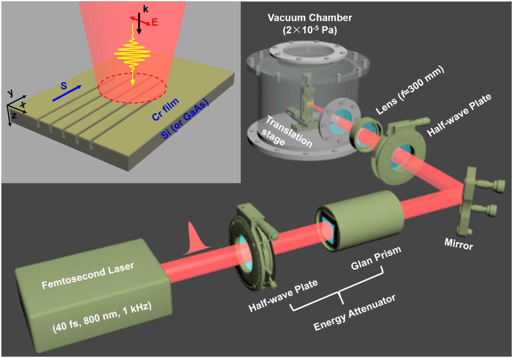
A schematic diagram for super-regular femtosecond laser nanolithography on the Cr/Si material based on dual-interface plasmonic coupling. Here, the sample is placed within a vacuum chamber with an air pressure of P = 2.0 × 10⁻⁵ Pa. The inset shows the superior formation of nanograting arrays via a line-scanning process. Here, k represents the wave vector of the incident laser; E for the electric-field vector or the polarization direction of the incident light, S for the direction of the sample scanning.
Figure 2(a) shows typical scanning electron microscope (SEM) images of the achieved surface structures on a sample material of 25 nm thick Cr/Si after irradiation with laser pulses at an energy E = 3.53 µJ (F = 22.5 mJ/cm2). It is clear that the sample surface exhibits 1D periodic grating-like structures with the remarkable uniformity of spatial distribution, which sharply contrasts with the observed features of bending, breaking, and bifurcation in traditional LIPSSs. The spatial orientation of these structures is always found to be perpendicular to the direction of the laser polarization [see Supplementary Material (S1)]. Importantly, such structural uniformity can be robustly extended over the whole laser scanning area, where a long-range spatial uniformity can be also identified by the fractional change of the structural period [see Supplementary Material (S2)]. Moreover, the dynamic formation ranges of the uniform structures are also experimentally investigated in terms of the laser fluence and scanning velocity. It was found that the grating structures show great stability to the laser parameters [see Supplementary Material (S3)]. From the corresponding magnified SEM images, we can find that the grating structures are composed of the periodical ablative grooves. The spatial period of these groove structures is measured to be as small as Λ25 = 355 ± 4 nm, less than half of the incident laser wavelength (800 nm). Moreover, for each ablated groove, two sharp cutting edges are clearly identified in accompany with numerous nanoscale grains aggregated on the nearby ridges. The observation of rough grating surface is supposed to result from the deposition of molten materials flowing out of the ablated grooves onto the nearby ridges, which subsequently develops into the quasi-periodic nanograins due to Rayleigh-Plateau liquid instability [35]. Figure 2(b) shows an image of the two-dimensional fast Fourier transformation (2D-FFT) of the nanograting structures, where the tiny spots in alignment indicate the high spatial regularity of the structural distribution. The measured frequency interval of f = 2.84 µm−1 between the adjacent spots corresponds to an average spatial period of 1/f = 352 nm, matching well with the direct measurement from the SEM image.
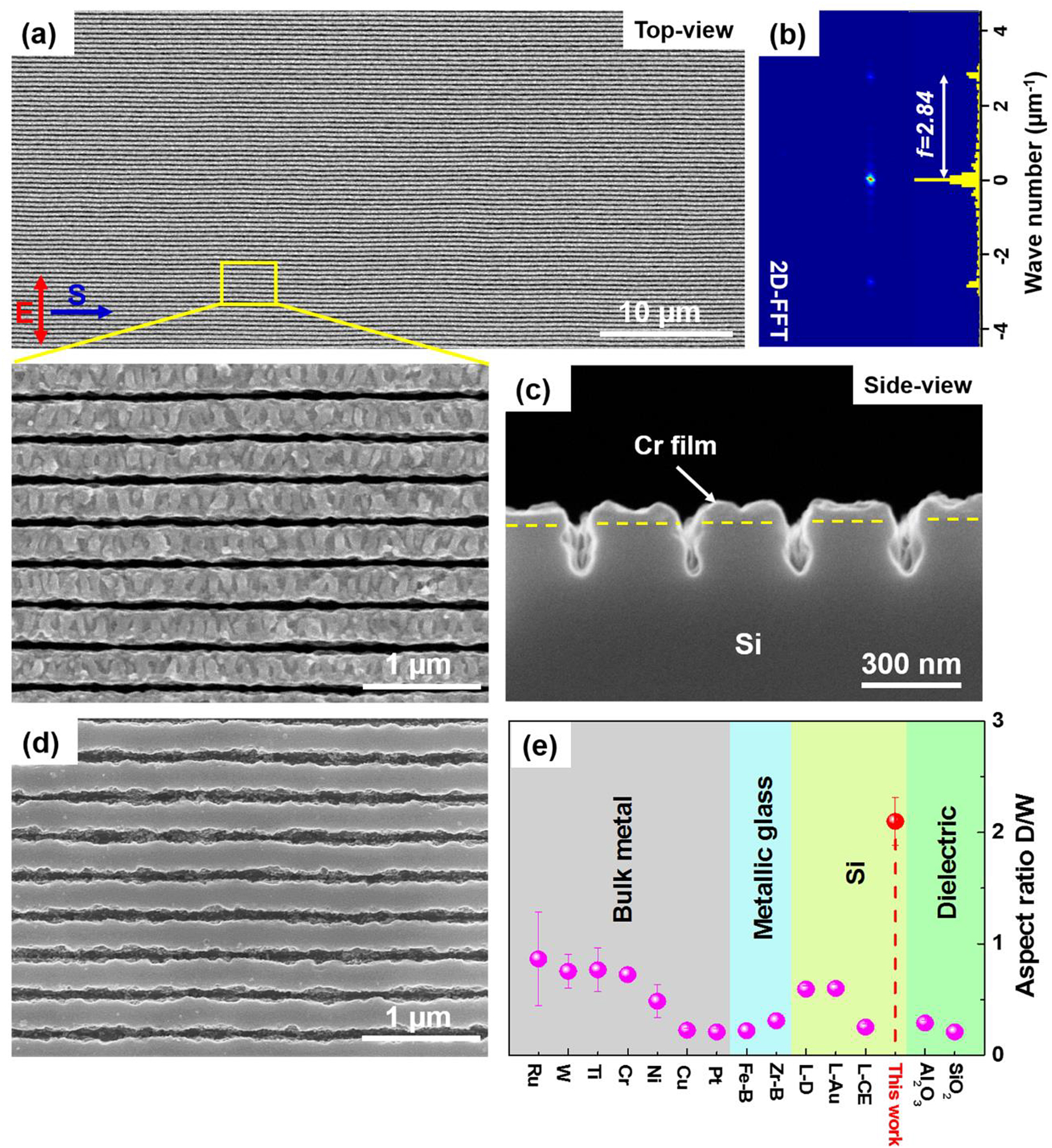
(a) SEM images (top view) of the laser-induced ablative nanograting structures on the surface of 25 nm thick Cr/Si sample. E and S represent the direction of the light polarization and sample scanning. (b) Calculated 2D-FFT image of the ablated grating structures, indicating a highly regular arrangement of the groove structures with a spatial period of 352 nm. (c) SEM image (side view) of the laser-induced nanograting structures, exhibiting an anomalously narrow-necked cross-sectional profile and a penetrating ablation into the Si substrate. (d) SEM image of the laser-induced nanograting structures on the Si substrate after removing 25 nm thick Cr layer by a Cr etchant solution. (e) Illustration of the depth-to-width aspect ratios for reported laser-induced nanograting structures and the Si nanograting structures in our work. Here, Fe-B and Zr-B represent Fe-based and Zr-based metallic glass, respectively; L-D for LIPSSs on the Si material directly processed by femtosecond laser pulses; L-Au for LIPSSs on the Si material coated with Au films; L-CE for LIPSSs on the Si material processed by the chemical etching assisted femtosecond laser modification.
Figure 2(c) depicts a side-view SEM image of the laser-induced grating structures. Interestingly, the ablated grooves exhibit narrow-necked profiles with a large width at both ends and a small width in the middle region, rather than the sinusoidal geometry usually observed on the surface of bulk materials [36], [37], [38]. More importantly, such fine grating structures are found to be deeply imprinted into the underlying Si substrate instead of restricting to the upper Cr layer. Remarkably, when the residual Cr films were removed by the Cr etchant solution, the Si nanograting structures exhibit an ultra-smooth and clean surface without ablation debris, as shown in Figure 2(d), much different from the surface of LIPSSs produced by direct irradiation of femtosecond laser pulses. The groove width and depth of the Si nanograting structures are measured to be W = 85 ± 7 nm and D = 178 ± 9 nm, respectively, exhibiting a large depth-to-width aspect ratio of γ = D/W = 2.1. In comparison with the reported LIPSSs on different materials [18, 21, 36], [37], [38], [39], [40], [41], [42], [43], [44], [45], the aspect ratio of Si nanograting structures in our experiments presents a considerably large value, as shown in Figure 2(e). In addition, our experiments further confirmed that such peculiar structures can be also formed on other substrates coated with thin Cr film, such as Si (110) or GaAs, which indicates the extensibility of our technique [see Supplementary Material (S4)]. In general, the Cr-layer mediated Si nanograting structures are unique, much different from the observations on material surfaces directly irradiated by femtosecond laser pulses in ambient air.
2.2 Influence of the metal film thicknesses on the structure formation
We also carried out experiments on Cr films with different thicknesses t = 50 nm, 100 nm, and a Cr bulk using different laser fluences F = 24.0, 25.1, and 30.3 mJ/cm2, respectively, as shown in Figure 3(a)–(c). Clearly, from these outcomes, we can conclude that the spatial regularity of the laser-induced structures strongly depends on the film thickness. For example, for a film thickness of 50 nm, the surface structures still display a very similar high regularity to that of 25 nm thick Cr film. However, when the thickness of Cr film increases to 100 nm or the bulk dimension, the laser-induced structures begin to possess breaking and splitting phenomena. According to Ref. [46], a concept of the dispersion of structure orientation angles (DSOA) can be introduced to quantitatively characterize the structural regularity. The related results for the formed surface structures on different Cr film thicknesses are plotted in Figure 3(d). Each DSOA curve shows a peak value near 0° and quickly decays with the increasing angles, which indicates that the structural orientation is mainly concentrated in the horizontal direction. Specifically, a half-maximum-full-width value (δθ) of the DSOA curve can essentially represent the structural quality. The smaller the δθ is, the more regular the structures become. In our cases, the δθ value appears to increase with larger film thicknesses. Figure 3(e) illustrates some other reported δθ values for the typical configurations of LIPSSs [15, 18, 39, 47, 48]. It is evident that our obtained nanograting structures on 25 nm thick Cr/Si material exhibit a noteworthy spatial uniformity of δθ = 4 ± 0.5°. Furthermore, as the thickness of Cr metal film increases from 25 to 50 nm, and then 100 nm, the spatial period of the laser-induced structures shows a slowly decreasing trend with the measured values of Λ25 = 355 ± 4 nm, Λ50 = 323 ± 4 nm, and Λ100 = 292 ± 44 nm, respectively. However, for the bulk dimension of Cr material, the structural period dramatically increases up to Λbulk = 765 ± 29 nm.
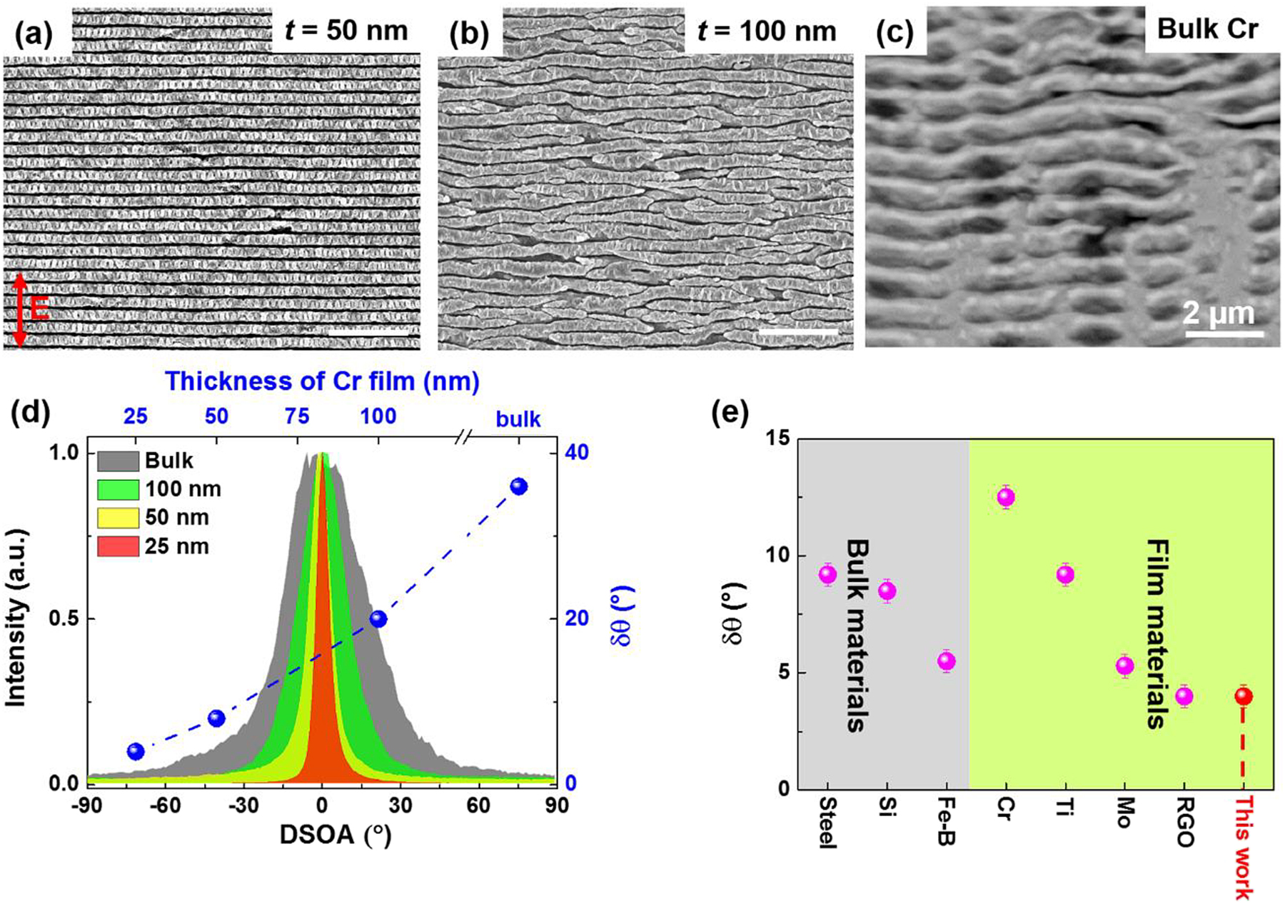
SEM images of the laser-induced surface structures on Cr films with different thicknesses.
(a) t = 50 nm, (b) t = 100 nm, and (c) bulk dimension. (d) Calculated DSOA curves and the corresponding half-maximum-full-width (δθ) values for the surface structure formation on different film thicknesses. (e) Summarization of the δθ values for the laser-induced structures reported in the published papers and formed on the 25 nm thick Cr/Si sample in our work. Here Fe-B indicates the material of Fe-based metallic glass; RGO for the reduced graphene oxide film.
2.3 Dual-interface plasmonic coupling for structure formation
The generally accepted mechanism for LIPSSs is attributed to the interference between the incident light and its excited SPPs. Under such circumstances, the incident Gaussian laser energy is first modulated into the periodic intensity fringes, and their ablation of the material surface subsequently results in the grating-like structures with a spatial orientation perpendicular to the direction of the laser polarization. This physical model works for the situation of the bulk Cr surface, in which the achieved structural period of Λbulk = 765 ± 29 nm nearly coincides with the single-interface SPP wavelength of 799 nm. However, this kind of physical picture does not provide a satisfactory explanation for the anomalous observations on the Cr/Si material; that is, the spatial period of the laser-induced structures is not only much smaller than that of the bulk material but also decreased with increasing the film thickness. To fully understand the underlying physics, we now provide an in-depth study of the laser-film interaction.
As for a thin metal film, hybrid SPP modes can be excited due to the perturbing effect of the lower interface upon the upper interface [49], which has been numerously demonstrated in both experiment and theory on noble metal films with tens of nanometers thickness [29, 50, 51]. The optical penetration depth of metal Cr is δ Cr = 18.4 nm at the wavelength of 800 nm, much larger than that of noble metals. Thus, it is feasible that two SPP modes are excited simultaneously at the upper and lower interfaces of a thin Cr film in our experiments, and then hybridize together generating dual-interface coupled plasmons. The dispersion relations of the dual-interface coupled SPPs are described in Supplementary Material (S5).
By solving the dispersion functions, with the parameters of ε 1 = 1, ε cr = −1.98 + i*21.88, and ε 3 = 13.65, we obtained two branches of the nonradiative mode for the dual-interface coupled plasmons, which are hereafter referred to as the hybrid SPP-1 and hybrid SPP-2 for the sake of convenience. Noticeably, the influence of nonequilibrium dynamics for Cr and Si materials on the excitation of hybrid SPPs can be negligible in our experiments [see Supplementary Material (S6)]. The calculated wavelengths of the two dual-interface coupled plasmons are dependent on the film thickness, as illustrated in Figure 4(a). Clearly, for the given range of thin-film thicknesses, the wavelength of the hybrid SPP-1 has smaller values compared to the case of hybrid SPP-2. With a gradual increase of the film thickness, the wavelength of the hybrid SPP-1 gradually reduces to 240 nm, which is almost identical to the individual SPP excitation on the Cr-Si interface. Analogously, the wavelength of the hybrid SPP-2 reaches 799 nm at larger film thicknesses, which is almost equal to the individual SPP excitation on the vacuum-Cr interface. More importantly, as shown in Figure 4(a), the measured structural periods for different Cr film thicknesses are in good agreement with the simulated wavelengths of the hybrid SPP-1, which indicates the underlying mechanism for our structure formation with the greatly reduced period. In addition, more evidence about the excitation of dual-interface coupled SPPs can be seen Supplementary Material (S5).
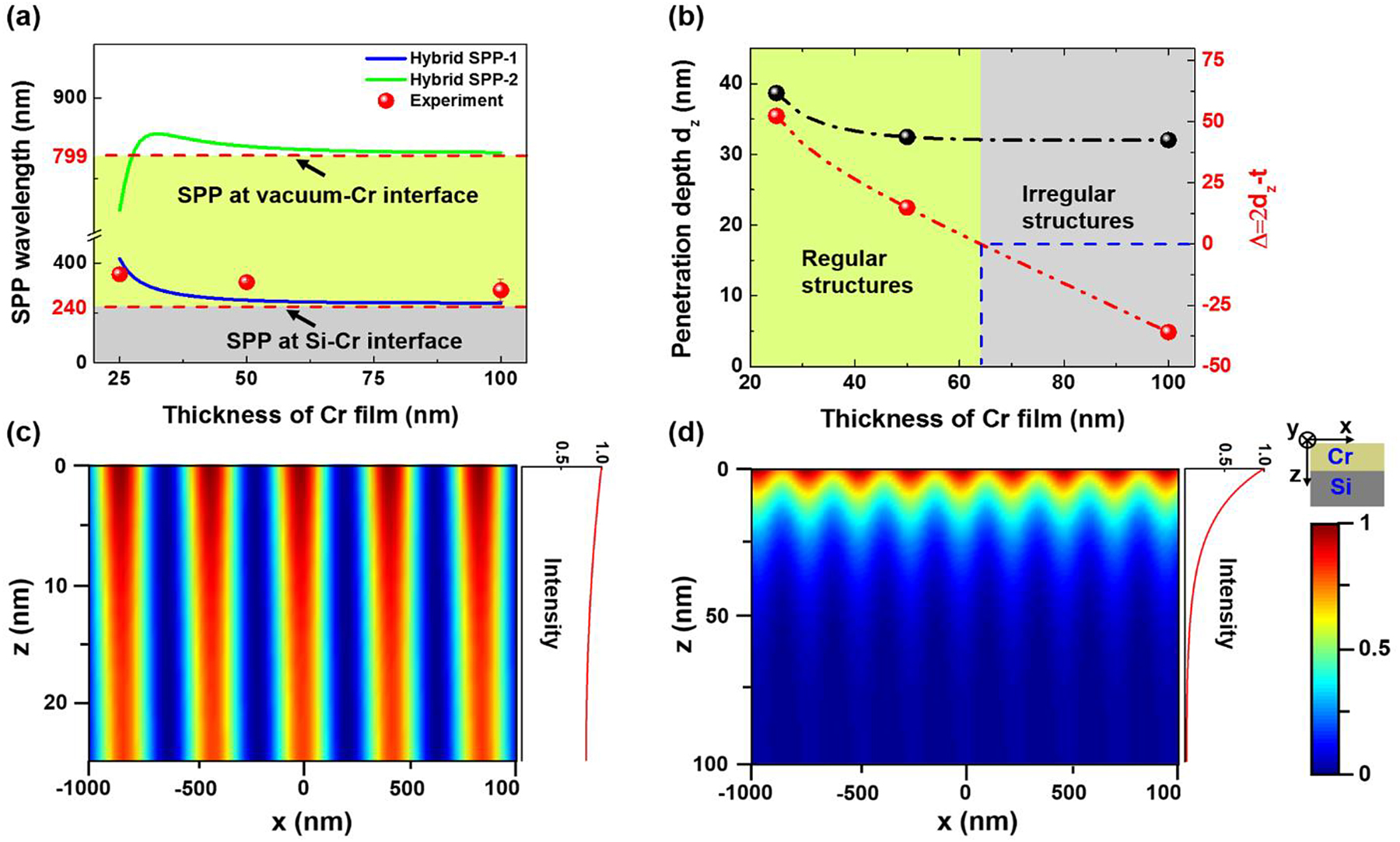
(a) Calculated wavelengths of the hybrid SPP-1 and SPP-2 versus the Cr film thickness. Red solid circles represent the measured period of the laser-induced structures on Cr metal film with different thicknesses. (b) Calculated optical penetration depths d z of the hybrid SPP-1 mode in Cr film (black color), and the values of Δ = 2d z − t (red color) as a function of the Cr film thickness t. The latter can be used for identifying the regular formation of the laser-induced structures. Simulations of spatially periodic intensity patterns from interference between the incident laser and the excited hybrid SPP-1 mode in Cr films with different thicknesses: (c) 25 nm (d) 100 nm.
The red curves on the right panels represent the retrieved intensity decaying situations along the film depth direction.
2.4 Physical origins of the structural regularity
Because of the complex physics involved, the spatial arrangement of the laser-induced structures can be affected by many factors. Recently, Iaroslav et al. reported that the regular formation of the surface structures is relevant to the spatial coherence of the excited SPPs, which could be easily preserved on a small irradiation area for a short SPP propagation length [15, 16]. However, we cannot simply use this concept to understand our experimental results, because the structural regularity becomes unsatisfactory for larger film thicknesses in spite of the bulk Cr material having a relatively short SPPs decay length of L SPP = 2.79 µm under 800 nm femtosecond laser irradiation. By comparing the experimental results of different film thicknesses with the calculated penetration depths d z of the hybrid SPP-1 mode, we can determine that the structure regularity is closely related to a physical parameter Δ = 2d z − t. Specifically, when Δ > 0, the laser-induced surface structures exhibit an exceptional spatial regularity; otherwise, the irregular formation of the structures becomes more apparent, as shown in Figure 4(b).
In order to elucidate the physical origins of the regular structure formation in the experiments, we simulated the spatial intensity distribution from interference between the incident laser and its excited hybrid SPP-1 for two different film thicknesses (t = 25 and 100 nm), as shown in Figure 4(c) and (d), respectively. In the case of 25 nm thick metal film (or Δ > 0), the resultant periodic intensity fringes starting from the upper surface are seen to extend across the whole Cr film with relatively homogeneous distribution, leading to the so-called periodic columnar intensity distribution (PCID). Within each PCID region, the optically excited hot electrons would like to rapidly transfer their energy to adjacent lattices via strong electron-phonon coupling, with negligible thermal diffusion due to the near homogenous energy distribution [52]. This results in the periodic slices of elevated lattice temperature throughout the thin film. When the ablation of Cr metal film occurs within the PCID regions, the escaped materials would like to take away most of the thermal energy and greatly diminish the residual heat in the film, leading to fewer molten traces left on the structures [53]. Notably, this kind of ablation cooling effect becomes more pronounced under the high vacuum environment, which can successfully explain the observation of sharp cutting edges for each ablated groove in the magnified SEM image of Figure 2(a).
Whereas, in the case of 100 nm thick film (i.e., Δ < 0), the simulated intensity of the periodic interference fringes is mainly located on the upper surface of the film (or the vacuum-Cr interface), and exponentially decays within an optical penetrating depth. Therefore, the spatially inhomogeneous intensity distribution is caused along the film depth direction, which is named as the point-spreading-like intensity distribution (PSID). Within each PSID region, the optically excited hot electrons on the surface would like to prominently diffuse into the greater depth due to the significant energy gradient, thus leading to a lowering of the energy density and lattice temperature. Furthermore, the ablation threshold increases for thicker films [54]. As a result, the amount of materials removed from the film becomes reduced. Accordingly, more residual thermal energy is left in the film to likely soften and melt the material with accompany of thermal instabilities, which finally gives rise to the external perturbations and stochastic disturbances on the structure arrangement [35]. In brief, the spatial distribution of laser-SPP interference intensities is highly dependent on the metal film thickness, which shows either nearly homogeneous depth-directional column profiles or the greatly inhomogeneous point spreading-like profiles. As a consequence, the severity of the electron diffusion within the localized energy regions determines the degree of material melting and the structure regularity.
2.5 Deepening of the nanograting structures into Si substrate
In our experiments, the ablative nanograting structures not only occur on the metal film but also deeply ablate into the Si substrate, reaching a total modulation depth of D total = 237 ± 22 nm. In order to fully understand the structuring process, we simulated the electric field distribution inside the columnar grooves with different depths under irradiation of subsequent femtosecond laser pulses using the Finite-Difference-Time-Domain (FDTD) method, and the corresponding results are shown in Figure 5(a)–(d). Here, the width and period of the grooves are given by 50 and 355 nm, respectively. The permittivity of Si material is taken as ε 3 = −4.95 + i*0.08 in consideration of the optically excited process [see Supplementary Material (S6)]. Clearly, for the relatively small groove depths (50–200 nm), the electric field enhancements more than 5 times are always seen to locate at the bottom of grooves, which make the main contribution to the continuous deepening process of grooves in spite of the high ablation threshold of nearly 200 mJ/cm2 for the Si substrate [55]. Moreover, the low air pressure environment (P = 2.0 × 10⁻⁵ Pa) is also beneficial to increase the groove depth via the acceleration of the ablation plume expansion and the suppression of the nanoparticle redeposition [56, 57]. However, at a relatively larger depth of 237 nm, a standing-wave-like electric field enhancement is found to appear in the longitudinal direction of grooves. The lower panel of Figure 5(d) shows that the electric field intensity is enhanced at least six-fold on two antinode positions marked by the dotted lines of A and B, respectively, which can seriously ablate the groove sidewalls resulting in the formation of anomalous narrow-necked geometry. Furthermore, our experiments also demonstrate that as the number of irradiating laser pulses further increases, the ablation regions on the groove sidewalls can be expanded again, eventually causing a collapse of groove ridges.
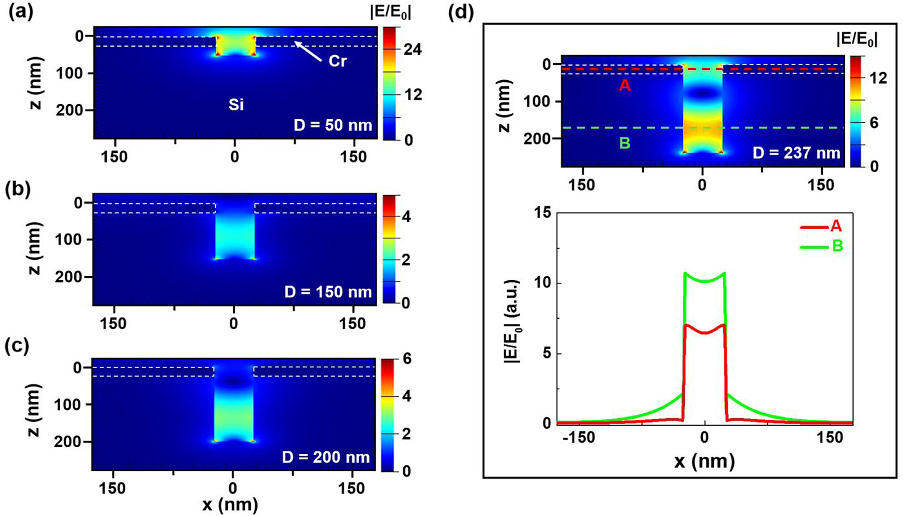
Simulations of the electric field distribution inside the columnar grooves with different depths under irradiation of femtosecond laser pulses.
(a) D = 50 nm, (b) D = 150 nm, (c) D = 200 nm, (d) D = 237 nm. The curves in the lower panel of (d) depict the electric field enhancement at two antinode positions marked by lines A and B in the upper panel of (d).
2.6 Angle-independent antireflection of structures on silicon
In this section, we employed a wet etching approach to further reduce the surface roughness and modify the structure geometry [see Supplementary Material (S7)]. Figure 6(a) and (b) shows the obtained Si nanograting structures after wet etching for 5 min, where the thin Cr layer was removed by the Cr etchant solution. Clearly, these structures are found to present an extremely smooth surface without the ablated debris or defects. Meanwhile, the cross-section of the grooves is modulated into a narrow-mouthed V-type profile (NMVP) with a mouth width of 202 nm. Undoubtedly, the generation of such exotic structure geometry originates from the laser-induced peculiar structures on the Si substrate, in sharp contrast to the formation of broad-mouthed V-shaped grooves by the traditional method [58]. Finally, the optical reflectivity of the periodic NMVP structures on the Si substrate was experimentally investigated using an angle-resolved micro-spectroscopy (ARMS, Ideaoptics), and the measured angular reflection (within a wavelength range of 400–1000 nm) for the p-polarized light is shown in Figure 6(c). It is seen that the optical reflection less than 10% is persistent for a relatively large incidence angle range (0–60°) in the spectrum range of 565–750 nm, in contrast to the previous studies of the antireflection measurement only concentrated at normal incidence [11, 12]. The remarkably decreased reflection extends much further away from the normal incidence, resulting in broadband near omnidirectional antireflection behaviors, which may have a great potential in Si-based solar cells. In physics, such angle-independent antireflection features are dominated by the efficient light trapping in NMVP structures [1, 59].
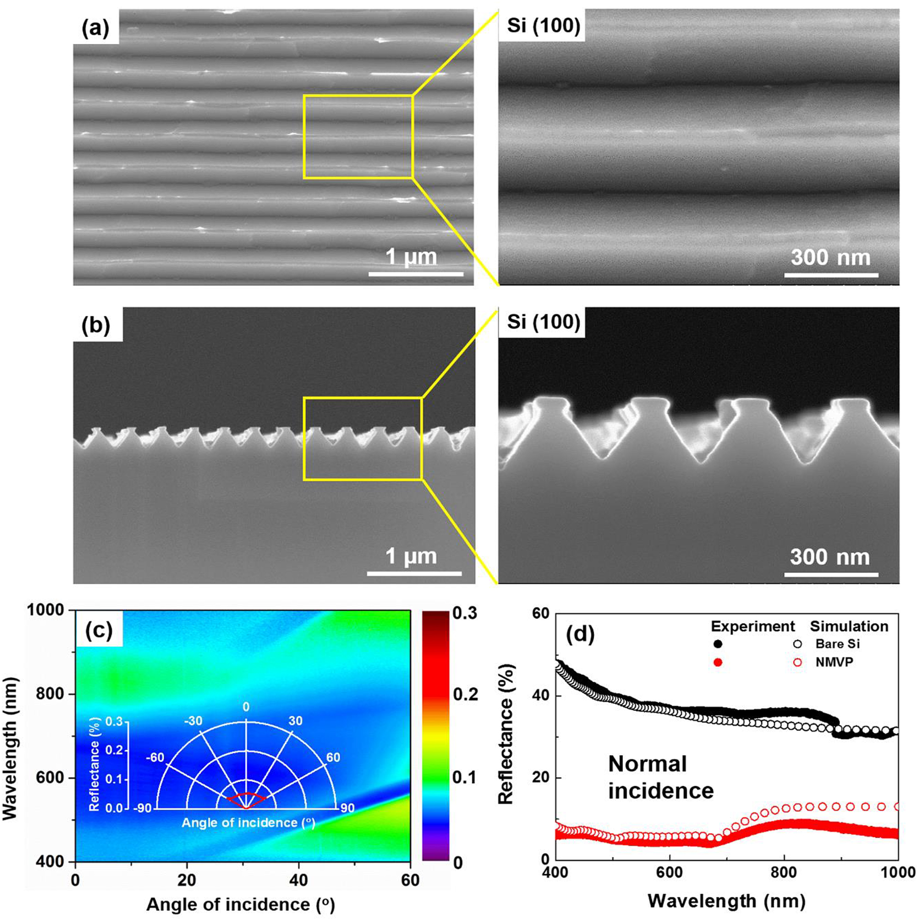
SEM images of the Si nanograting structures after wet etching for 5 min.
(a) Top-view and (b) side-view. (c) Measured incidence-angle dependence of the reflectance spectra for p-polarized light. The white polar coordinate illustrates the retrieved angular reflection intensity at the incident wavelength of 700 nm. (d) Measured (solid-circles) and simulated (void-circles) optical reflectivity for p-polarized light at normal incidence. Black: bare Si. Red: Si decorated with NMVP structures.
Figure 6(d) shows the optical reflection spectra for the NMVP structures at normal incidence. In comparison with the bare Si material, the optical reflection of the structured Si surface demonstrates an evident overall drop, especially down to only 5% in the visible wavelength range (565–750 nm), which is also smaller than that caused by the reported LIPSSs on Si material [11]. The calculated results show a good agreement with our measurement data. Moreover, the broadband antireflection performance was also found for s-polarized light, with the measured optical reflection values of approximately 25%.
3 Conclusions
In this work, a maskless and high-precision femtosecond laser surface structuring technique has been presented, involving the irradiation of 800 nm femtosecond laser on the Cr/Si material under high vacuum conditions. Using this technique, super-regular deep-subwavelength Si nanograting structures were achieved associated with an ultra-smooth surface and a large depth-to-width aspect ratio, which are hardly realized by direct femtosecond laser processing on the Si material. Importantly, the formation of such superior structures can be also generated on other semiconductor materials, indicating the extensibility of our technique. Besides, the spatial period and regular distribution of the nanograting structures were found to be closely dependent on the metal film thickness.
In theory, a physical model that involves the excitation of dual-interface coupled plasmons in thin metal films was proposed to explain the experimental observations. That is, the well-defined nanograting structures stem from the material ablation by the PCID patterns in the thin Cr film, in contrast to the PSID patterns in the thick Cr films. The parameter Δ = 2d z − t was defined as a criterion to identify the film thickness-dependent structure regularity. Moreover, the further deepening of structures into the Si material was also revealed by the simulation of the electric field inside the grooves under irradiation of subsequent laser pulses. With the assistance of wet etching, the Cr-layer mediated Si nanograting structures were further modified into the smooth NMVP structures, exhibiting a noticeable broadband angle-independent antireflection performance, especially in the spectrum range of 565–750 nm.
In conclusion, the thin Cr-layer mediated femtosecond laser lithography not only solved the common problem of irregular (or wavy) arrangement for LIPSSs at deep-subwavelength scales but also provided a novel method to fabricate the clean and smooth exotic structures on Si material for the efficient light trapping. Thus, we believe that it will be of interest to both fundamental science and practical applications.
4 Methods
A commercially available chirped pulse amplification of Ti:sapphire femtosecond laser system (Spectra-Physics HP-Spitfire 50) is employed for delivering horizontally polarized laser pulse trains at a repetition rate of 1 kHz. The central wavelength and time duration of the output laser pulses are λ = 800 nm and τ = 40 fs, respectively. The pulse energy is tuned by an energy attenuator that consists of a half-wave plate and a Glan prism, and the direction of the laser polarization is controlled by another half-wave plate. After that, the laser beam is focused by a lens (focal length: f = 300 mm; numerical aperture: N.A = 0.017) into a vacuum chamber with a magnesium fluoride (MgF2) window, in which a Cr/Si material (prepared by evaporating the thin Cr film onto an <100> oriented single crystal silicon) is mounted onto a three-dimensional translation stage. The selection of metallic Cr film is due to the large electron-phonon coupling coefficient (4.2 × 10¹⁷ W/m3 K), which can diminish the hot diffusion of electrons absorbing the laser energy and benefit the formation of LIPSSs [52]. The sample surface is positioned approximately 4 mm before the laser focus, on which the beam spot diameter is around φ = 141.4 µm (1/e 2 intensity). The average pulse fluence F is calculated following the traditional formula of F = 4E/(πφ 2), where E is the single pulse energy. During experiments, the sample is scanned perpendicular to the propagation direction of the laser beam with a slow velocity of V = 2 μm/s, producing nearly N = 7.1 × 10⁴ pulses that partially overlap within one spot area. The air in the chamber is exhausted down to the low pressure of P = 2.0 × 10⁻⁵ Pa, which can effectively prohibit the oxidation of Cr films during laser irradiation [see Supplementary Material (S8)]. The morphology of the laser-exposed surface is characterized by a scanning electron microscope (SEM, HITACHI, S-4800).
Funding source: National Natural Science Foundation of China http://dx.doi.org/10.13039/501100001809
Award Identifier / Grant number: 11674178
Award Identifier / Grant number: 11804334
Award Identifier / Grant number: 91750205
Funding source: K. C. Wong Education Foundation
Award Identifier / Grant number: GJTD-2018-08
Funding source: Jilin Provincial Science & Technology Development Project http://dx.doi.org/10.13039/100007847
Award Identifier / Grant number: 20180414019GH
Acknowledgment
The authors appreciate Chunlei Guo for the technical supports, Dandan Yan and Fei Xie for the preparation of experimental samples, and Yuhao Lei for the critical reading and comments support.
-
Author contributions: All the authors have accepted responsibility for the entire content of this submitted manuscript and approved submission.
-
Research funding: National Natural Science Foundation of China (Grant Nos. 91750205, 11674178, and 11804334); Jilin Provincial Science & Technology Development Project (Grant No. 20180414019GH); K. C. Wong Education Foundation (GJTD-2018-08).
-
Conflict of interest statement: The authors declare no competing financial interest.
References
[1] T. V. Teperik, F. J. Garciadeabajo, Y. Sugawara, and J. J. Baumberg, “Omnidirectional absorption in nanostructured metal surfaces,” Nat. Photonics, vol. 2, pp. 299–301, 2008, https://doi.org/10.1038/nphoton.2008.76.Search in Google Scholar
[2] T. Ebbesen, H. ELezec, H. Ghaemi, T. Thio, and P. Wolff, “Extraordinary optical transmission through sub-wavelength hole arrays,” Nature, vol. 391, pp. 667–669, 1998, https://doi.org/10.1038/35570.Search in Google Scholar
[3] X. Du and R. Jin, “Atomically precise metal nanoclusters for catalysis,” ACS Nano, vol. 13, pp. 7383–7387, 2019, https://doi.org/10.1021/acsnano.9b04533.Search in Google Scholar PubMed
[4] D. Wang, Q. Liu, Q. Sun, et al.., “Design of robust superhydrophobic surfaces,” Nature, vol. 582, pp. 55–59, 2020, https://doi.org/10.1038/s41586-020-2331-8.Search in Google Scholar PubMed
[5] Y. Chen and A. Pepin, “Nanofabrication: conventional and nonconventional methods,” Electrophoresis, vol. 22, pp. 187–207, 2001, https://doi.org/10.1002/1522-2683(200101)22:2<187::aid-elps187>3.0.co;2-0.10.1002/1522-2683(200101)22:2<187::AID-ELPS187>3.0.CO;2-0Search in Google Scholar
[6] B. Gates, Q. Xu, M. Stewart, D. Ryan, C. Willson, and G. Whitesides, “New approaches to nanofabrication: molding, printing, and other techniques,” Chem. Rev., vol. 105, pp. 1171–1196, 2005, https://doi.org/10.1021/cr030076o.Search in Google Scholar
[7] R. Pease and S. Chou, “Lithography and other patterning techniques for future electronics,” Proc. IEEE, vol. 96, pp. 248–270, 2008, https://doi.org/10.1109/jproc.2007.911853.Search in Google Scholar
[8] J. Wang and C. Guo, “Ultrafast dynamics of femtosecond laser-induced periodic surface pattern formation on metals,” Appl. Phys. Lett., vol. 87, p. 251914, 2005, https://doi.org/10.1063/1.2146067.Search in Google Scholar
[9] A. Borowiec and H. K. Haugen, “Subwavelength ripple formation on the surfaces of compound semiconductors irradiated with femtosecond laser pulses,” Appl. Phys. Lett., vol. 82, pp. 4462–4464, 2003, https://doi.org/10.1063/1.1586457.Search in Google Scholar
[10] Q. Wu, Y. Ma, R. Fang, Y. Liao, and Q. Yu, “Femtosecond laser-induced periodic surface structure on diamond film,” Appl. Phys. Lett., vol. 82, pp. 1703–1705, 2003, https://doi.org/10.1063/1.1561581.Search in Google Scholar
[11] A. Y. Vorobyev and C. Guo, “Antireflection effect of femtosecond laser-induced periodic surface structures on silicon,” Opt. Express, vol. 19, pp. A1031–A1036, 2011, https://doi.org/10.1364/oe.19.0a1031.Search in Google Scholar
[12] C. Yao, Y. Ye, B. Jia, et al.., “Polarization and fluence effects in femtosecond laser induced micro/nano structures on stainless steel with antireflection property,” Appl. Surf. Sci., vol. 425, pp. 1118–1124, 2017, https://doi.org/10.1016/j.apsusc.2017.07.157.Search in Google Scholar
[13] A. Cerkauskaite, R. Drevinskas, A. Solodar, I. Abdulhalim, and P. G. Kazansky, “Form-birefringence in ITO thin films engineered by ultrafast laser nanostructuring,” ACS Photonics, vol. 4, pp. 2944–2951, 2017, https://doi.org/10.1021/acsphotonics.7b01082.Search in Google Scholar
[14] J. Bonse, R. Koter, M. Hartelt, et al.., “Femtosecond laser-induced periodic surface structures on steel and titanium alloy for tribological applications,” Appl. Phys. A, vol. 117, pp. 103–110, 2014, https://doi.org/10.1007/s00339-014-8229-2.Search in Google Scholar
[15] I. Gnilitskyi, T. J. Y. Derrien, Y. Levy, N. M. Bulgakova, T. Mocek, and L. Orazi, “High-speed manufacturing of highly regular femtosecond laser-induced periodic surface structures: physical origin of regularity,” Sci. Rep., vol. 7, p. 8485, 2017, https://doi.org/10.1038/s41598-017-08788-z.Search in Google Scholar PubMed PubMed Central
[16] B. Öktem, I. Pavlov, S. Ilday, et al.., “Nonlinear laser lithography for indefinitely large-area nanostructuring with femtosecond pulses,” Nat. Photonics, vol. 7, pp. 897–901, 2013, https://doi.org/10.1038/nphoton.2013.272.Search in Google Scholar
[17] Q. Liu, N. Zhang, J. Yang, H. Qiao, and C. Guo, “Direct fabricating large-area nanotriangle structure arrays on tungsten surface by nonlinear lithography of two femtosecond laser beams,” Opt. Express, vol. 26, pp. 11718–11727, 2018.https://doi.org/10.1364/OE.26.011718.Search in Google Scholar PubMed
[18] Y. Lei, J. Yang, C. Cong, and C. Guo, “Fabrication of homogenous subwavelength grating structures on metallic glass using double-pulsed femtosecond lasers,” Opt. Laser. Eng., vol. 134, p. 106273, 2020, https://doi.org/10.1016/j.optlaseng.2020.106273.Search in Google Scholar
[19] X. Zheng, B. Zhao, J. Yang, Y. Lei, T. Zou, and C. Guo, “Noncollinear excitation of surface plasmons for triangular structure formation on Cr surfaces by femtosecond lasers,” Appl. Surf. Sci., vol. 507, p. 144932, 2020, https://doi.org/10.1016/j.apsusc.2019.144932.Search in Google Scholar
[20] M. Garcia-Lechuga, D. Puerto, Y. Fuentes-Edfuf, J. Solis, and J. Siegel, “Ultrafast moving-spot microscopy: birth and growth of laser-induced periodic surface structures,” ACS Photonics, vol. 3, pp. 1961–1967, 2016, https://doi.org/10.1021/acsphotonics.6b00514.Search in Google Scholar
[21] J. Huang, L. Jiang, X. Li, et al.., “Fabrication of highly homogeneous and controllable nanogratings on silicon via chemical etching-assisted femtosecond laser modification,” Nanophotonics, vol. 8, pp. 869–878, 2019, https://doi.org/10.1515/nanoph-2019-0056.Search in Google Scholar
[22] J. Huang, L. Jiang, X. Li, et al.., “Cylindrically focused nonablative femtosecond laser processing of long‐range uniform periodic surface structures with tunable diffraction efficiency,” Adv. Opt. Mater., vol. 7, p. 1900706, 2019, https://doi.org/10.1002/adom.201900706.Search in Google Scholar
[23] Y. Zhang, Q. Jiang, K. Cao, et al.., “Extremely regular periodic surface structures in a large area efficiently induced on silicon by temporally shaped femtosecond laser,” Photonics Res., vol. 9, p. 839, 2021, https://doi.org/10.1364/prj.418937.Search in Google Scholar
[24] E. V. Golosov, A. A. Ionin, Y. R. Kolobov, et al.., “Ultrafast changes in the optical properties of a titanium surface and femtosecond laser writing of one-dimensional quasi-periodic nanogratings of its relief,” J. Exp. Theor. Phys., vol. 113, pp. 14–26, 2011, https://doi.org/10.1134/s1063776111050025.Search in Google Scholar
[25] M. Huang, F. Zhao, Y. Cheng, N. Xu, and Z. Xu, “Origin of laser-induced near-subwavelength ripples: interference between surface plasmons and incident laser,” ACS Nano, vol. 3, pp. 4062–4070, 2009, https://doi.org/10.1021/nn900654v.Search in Google Scholar PubMed
[26] S. Sakabe, M. Hashida, S. Tokita, S. Namba, and K. Okamuro, “Mechanism for self-formation of periodic grating structures on a metal surface by a femtosecond laser pulse,” Phys. Rev. B, vol. 79, p. 033409, 2009, https://doi.org/10.1103/physrevb.79.033409.Search in Google Scholar
[27] W. L. Barnes, D. Alain, and T. W. Ebbesen, “Surface plasmon subwavelength optics,” Nature, vol. 424, pp. 824–830, 2003, https://doi.org/10.1038/nature01937.Search in Google Scholar PubMed
[28] J. J. Burke, G. I. Stegeman, and T. Tamir, “Surface-polariton-like waves guided by thin, lossy metal films,” Phys. Rev. B, vol. 33, pp. 5186–5201, 1986, https://doi.org/10.1103/physrevb.33.5186.Search in Google Scholar PubMed
[29] B. Frank, P. Kahl, D. Podbiel, et al.., “Short-range surface plasmonics: localized electron emission dynamics from a 60-nm spot on an atomically flat single-crystalline gold surface,” Sci. Adv., vol. 3, p. e1700721, 2017, https://doi.org/10.1126/sciadv.1700721.Search in Google Scholar PubMed PubMed Central
[30] F. Yang, J. R. Sambles, and G. W. Bradberry, “Long-range surface modes supported by thin films,” Phys. Rev. B, vol. 44, pp. 5855–5872, 1991, https://doi.org/10.1103/physrevb.44.5855.Search in Google Scholar PubMed
[31] K. MacDonald, Z. Samson, M. Stockman, and N. Zheludev, “Ultrafast active plasmonics,” Nat. Photonics, vol. 3, pp. 55–58, 2009, https://doi.org/10.1038/nphoton.2008.249.Search in Google Scholar
[32] Q. Min, C. Chen, P. Berini, and R. Gordon, “Long range surface plasmons on asymmetric suspended thin film structures for biosensing applications,” Opt. Express, vol. 18, pp. 19009–19019, 2010, https://doi.org/10.1364/oe.18.019009.Search in Google Scholar PubMed
[33] T. Derrien, R. Koter, J. Kruger, S. Hohm, A. Rosenfeld, and J. Bonse, “Plasmonic formation mechanism of periodic 100-nm-structures upon femtosecond laser irradiation of silicon in water,” J. Appl. Phys., vol. 116, p. 074902, 2014, https://doi.org/10.1063/1.4887808.Search in Google Scholar
[34] A. V. Dostovalov, T. J. Y. Derrien, S. A. Lizunov, et al.., “LIPSS on thin metallic films: new insights from multiplicity of laser-excited electromagnetic modes and efficiency of metal oxidation,” Appl. Surf. Sci., vol. 491, pp. 650–658, 2019, https://doi.org/10.1016/j.apsusc.2019.05.171.Search in Google Scholar
[35] J. D. Fowlkes, L. Kondic, J. Diez, Y. Wu, and P. D. Rack, “Self-assembly versus directed assembly of nanoparticles via pulsed laser induced dewetting of patterned metal films,” Nano Lett., vol. 11, pp. 2478–2485, 2011, https://doi.org/10.1021/nl200921c.Search in Google Scholar PubMed
[36] J. P. Colombier, F. Garrelie, N. Faure, et al.., “Effects of electron-phonon coupling and electron diffusion on ripples growth on ultrafast-laser-irradiated metals,” J. Appl. Phys., vol. 111, p. 024902, 2012, https://doi.org/10.1063/1.3676221.Search in Google Scholar
[37] M. H. Dar, R. Kuladeep, and V. Saikiran, “Femtosecond laser nanostructuring of titanium metal towards fabrication of low-reflective surfaces over broad wavelength range,” Appl. Surf. Sci., vol. 371, pp. 479–487, 2016, https://doi.org/10.1016/j.apsusc.2016.03.008.Search in Google Scholar
[38] A. Y. Vorobyev, V. S. Makin, and C. Guo, “Periodic ordering of random surface nanostructures induced by femtosecond laser pulses on metals,” J. Appl. Phys., vol. 101, p. 034903, 2007, https://doi.org/10.1063/1.2432288.Search in Google Scholar
[39] A. Ruiz de la Cruz, R. Lahoz, J. Siegel, G. F. Fuente, and J. Solis, “High speed inscription of uniform, large-area laser-induced periodic surface structures in Cr films using a high repetition rate fs laser,” Opt. Lett., vol. 39, pp. 2491–2494, 2014, https://doi.org/10.1364/ol.39.002491.Search in Google Scholar
[40] W. Zhang, G. Cheng, X. D. Hui, and Q. Feng, “Abnormal ripple patterns with enhanced regularity and continuity in a bulk metallic glass induced by femtosecond laser irradiation,” Appl. Phys. A, vol. 115, pp. 1451–1455, 2014, https://doi.org/10.1007/s00339-013-8062-z.Search in Google Scholar
[41] L. Hong, Rusli, X. C. Wang, H. Y. Zheng, H. Wang, and H. Y. Yu, “Femtosecond laser fabrication of large-area periodic surface ripple structure on Si substrate,” Appl. Surf. Sci., vol. 297, pp. 134–138, 2014, https://doi.org/10.1016/j.apsusc.2014.01.100.Search in Google Scholar
[42] P. Feng, L. Jiang, X. Li, W. Rong, K. Zhang, and Q. Cao, “Gold-film coating assisted femtosecond laser fabrication of large-area, uniform periodic surface structures,” Appl. Opt., vol. 54, p. 1314, 2015, https://doi.org/10.1364/ao.54.001314.Search in Google Scholar
[43] S. Schwarz, S. Rung, C. Esen, and R. Hellmann, “Homogeneous low spatial frequency LIPSS on dielectric materials generated by beam-shaped femtosecond pulsed laser irradiation,” J. Laser Micro Nanoeng., vol. 13, pp. 90–94, 2018, https://doi.org/10.2961/jlmn.2018.02.0007.Search in Google Scholar
[44] Q. Liang, Y. Zhong, Z. Fan, et al.., “Optical transmission during mid-infrared femtosecond laser pulses ablation of fused silica,” Appl. Surf. Sci., vol. 471, pp. 506–515, 2019, https://doi.org/10.1016/j.apsusc.2018.11.192.Search in Google Scholar
[45] S. I. Kudryashov, A. A. Nastulyavichus, I. N. Saraeva, A. A. Rudenko, D. A. Zayarny, and A. A. Ionin, “Deeply sub-wavelength laser nanopatterning of Si surface in dielectric fluids: manipulation by surface plasmon resonance,” Appl. Surf. Sci., vol. 519, p. 146204, 2020, https://doi.org/10.1016/j.apsusc.2020.146204.Search in Google Scholar
[46] J. Schindelin, C. T. Rueden, M. C. Hiner, and K. W. Eliceiri, “The ImageJ ecosystem: An open platform for biomedical image analysis,” Mol. Reprod. Dev., vol. 82, pp. 518–529, 2015, https://doi.org/10.1002/mrd.22489.Search in Google Scholar PubMed PubMed Central
[47] L. Wang, Q. D. Chen, X. W. Cao, et al.., “Plasmonic nano-printing: large-area nanoscale energy deposition for efficient surface texturing,” Light Sci. Appl., vol. 6, p. e17112, 2017, https://doi.org/10.1038/lsa.2017.112.Search in Google Scholar PubMed PubMed Central
[48] T. Zou, B. Zhao, W. Xin, et al.., “High-speed femtosecond laser plasmonic lithography and reduction of graphene oxide for anisotropic photoresponse,” Light Sci. Appl., vol. 9, p. 69, 2020, https://doi.org/10.1038/s41377-020-0311-2.Search in Google Scholar PubMed PubMed Central
[49] P. Ferguson, F. Wallis, and G. Chauvet, “Surface plasma waves in the noble metals,” Surf. Sci., vol. 82, pp. 255–269, 1979, https://doi.org/10.1016/0039-6028(79)90333-9.Search in Google Scholar
[50] A. Paliwal, M. Tomar, and V. Gupta, “Refractive index sensor using long-range surface plasmon resonance with prism coupler,” Plasmonics, vol. 14, pp. 375–381, 2018, https://doi.org/10.1007/s11468-018-0814-3.Search in Google Scholar
[51] J. C. Quail, J. G. Rako, and H. J. Simon, “Long-range surface-plasmon modes in silver and aluminum films,” Opt. Lett., vol. 8, pp. 377–379, 1983, https://doi.org/10.1364/ol.8.000377.Search in Google Scholar PubMed
[52] J. Hohlfeld, S. Wellershoff, J. Gudde, U. Conrad, V. Jahnke, and E. Matthias, “Electron and lattice dynamics following optical excitation of metals,” Chem. Phys., vol. 251, pp. 237–258, 2000, https://doi.org/10.1016/s0301-0104(99)00330-4.Search in Google Scholar
[53] C. Kerse, H. Kalaycioglu, P. Elahi, et al.., “Ablation-cooled material removal with ultrafast bursts of pulses,” Nature, vol. 537, pp. 84–88, 2016, https://doi.org/10.1038/nature18619.Search in Google Scholar PubMed
[54] S. Wellershoff, J. Hohlfeld, J. Gudde, and E. Matthias, “The role of electron-phonon coupling in femtosecond laser damage of metals,” Appl. Phys. A, vol. 69, pp. S99–S107, 1999, https://doi.org/10.1007/s003399900305.Search in Google Scholar
[55] L. Jiang, W. Han, X. Li, Q. Wang, F. Meng, and Y. Lu, “Crystal orientation dependence of femtosecond laser-induced periodic surface structure on (100) silicon,” Opt. Lett., vol. 39, pp. 3114–3117, 2014, https://doi.org/10.1364/ol.39.003114.Search in Google Scholar
[56] S. Juodkazis, H. Okuno, N. Kujime, S. Matsuo, and H. Misawa, “Hole drilling in stainless steel and silicon by femtosecond pulses at low pressure,” Appl. Phys. A, vol. 79, pp. 1555–1559, 2004, https://doi.org/10.1007/s00339-004-2846-0.Search in Google Scholar
[57] J. Jj Nivas, F. Gesuele, E. Allahyari, et al.., “Effects of ambient air pressure on surface structures produced by ultrashort laser pulse irradiation,” Opt. Lett., vol. 42, pp. 2710–2713, 2017, https://doi.org/10.1364/ol.42.002710.Search in Google Scholar PubMed
[58] A. Mavrokefalos, S. E. Han, S. Yerci, M. S. Branham, and G. Chen, “Efficient light trapping in inverted nanopyramid thin crystalline silicon membranes for solar cell applications,” Nano Lett., vol. 12, pp. 2792–2796, 2012, https://doi.org/10.1021/nl2045777.Search in Google Scholar PubMed
[59] A. Wirgin and A. Maradudin, “Resonant enhancement of the electric field in the grooves of bare metallic gratings exposed to S-polarized light,” Phys. Rev. B, vol. 31, pp. 5573–5576, 1985, https://doi.org/10.1103/physrevb.31.5573.Search in Google Scholar PubMed
Supplementary Material
The online version of this article offers supplementary material (https://doi.org/10.1515/nanoph-2021-0329).
Influence of laser polarization on the nanograting formation, Characterizations of the long-range spatial uniformity, Influences of laser fluence and scanning velocity on the nanograting formation, Extensibility of the nanograting structures on other substrate materials, Excitation of dual-interface coupled SPPs in thin Cr films, Influence of ultrafast dynamics of materials on the excitation of hybrid SPPs, Wet etching assisted modification of Si nanograting structures, Analysis of material compositions for nanograting structures (word).
© 2021 Hongbo Xie et al., published by De Gruyter, Berlin/Boston
This work is licensed under the Creative Commons Attribution 4.0 International License.
Articles in the same Issue
- Frontmatter
- Review
- Femtosecond laser micromachining for integrated quantum photonics
- Research Article
- Synthetic plasmonic lattice formation through invariant frequency comb excitation in graphene structures
- Nearly total optical transmission of linearly polarized light through transparent electrode composed of GaSb monolithic high-contrast grating integrated with gold
- Super-regular femtosecond laser nanolithography based on dual-interface plasmons coupling
- Inverse design of grating couplers using the policy gradient method from reinforcement learning
- Exfoliated Bi2Te3 nanoparticle suspensions and films: morphological and nonlinear optical characterization
- Experimental demonstration of broadband negative refraction at visible frequencies by critical layer thickness analysis in a vertical hyperbolic metamaterial
- Sensitive THz sensing based on Fano resonance in all-polymeric Bloch surface wave structure
- Photonic crystal nanobeam cavities with lateral fins
- Spectral tuning of diamond photonic crystal slabs by deposition of a thin layer with silicon vacancy centers
- Tailoring of plasmonic functionalized metastructures to enhance local heating release
- Fourier-component engineering to control light diffraction beyond subwavelength limit