Few picosecond dynamics of intraband transitions in THz HgTe nanocrystals
-
Thibault Apretna


Abstract
Optoelectronic devices based on intraband or intersublevel transitions in semiconductors are important building blocks of the current THz technology. Large nanocrystals (NCs) of Mercury telluride (HgTe) are promising semiconductor candidates owing to their intraband absorption peak tunable from 60 THz to 4 THz. However, the physical nature of this THz absorption remains elusive as, in this spectral range, quantum confinement and Coulomb repulsion effects can coexist. Further, the carrier dynamics at low energy in HgTe NCs, which strongly impact the performances of THz optoelectronic devices, is still unexplored. Here, we demonstrate a broad THz absorption resonance centered at ≈4.5 THz and fully interpret its characteristics with a quantum model describing multiple intraband transitions of single carriers between quantized states. Our analysis reveals the absence of collective excitations in the THz optical response of these self-doped large NCs. Furthermore, using optical pump-THz probe experiments, we report on carrier dynamics at low energy as long as 6 ps in these self-doped THz HgTe NCs. We highlight evidence that Auger recombination is irrelevant in this system and attribute the main carrier recombination process to direct energy transfer from the electronic transition to the ligand vibrational modes and to nonradiative recombination assisted by surface traps. Our study opens interesting perspectives for the use of large HgTe NCs for the development of advanced THz optoelectronic devices such as emitters and detectors and for quantum engineering at THz frequencies.
1 Introduction
Mercury telluride (HgTe) nanocrystals [1] (NCs) appear as a promising active material for low-cost infrared sensors [2]. In its bulk form, HgTe is a zero-band gap semiconductor, which means that the bandgap of HgTe NCs can potentially be reduced to zero eV [3], unlike infrared NCs such as lead chalcogenides that have their tunability limited by the bulk bandgap (≈0.4 eV for PbS) [4]. Over the past decade, rapid progress has been realized on the colloidal growth of HgTe NCs. Rogach et al. were the first to report the growth of such narrow bandgap II–VI NCs and obtained very small particles with a bandgap corresponding to 1300 nm [5]. The addition of a ripening step allowed Kovalenko et al. to push the absorption beyond the telecom range and reach 3 µm [6]. Later Keuleyan et al. reported absorption edges up to 5 µm [7], which can be extended up to 12 µm by the addition of a regrowth step [8]. Recently, Goubet et al. developed a high-temperature procedure for HgTe NCs in order to push the absorption of NCs to 200 µm (i.e. 1.5 THz) [9]. Such long-wavelength absorption is enabled by the growth of large NCs (up to 1 µm) with sizes above the HgTe Bohr radius (40 nm) [10]. While intensive efforts have been dedicated to the synthesis and device integration of short-wave [11, 12] and mid-wave [7, 13, 14] infrared NCs, very little work has to date been focused on the investigation of the electronic structure, charge transport, and optical properties of mercury chalcogenide THz NCs [10, 15].
In such large nanoparticles, the absorption spectrum presents interband absorption at high energy and a peak at low energy that is the signature of self-doping [16–19]. This doping mechanism is specific to narrow bandgap NCs and corresponds to a reduction of the NCs by the environment as the low confinement brings the Fermi level above the ground state of the conduction band (1 Se state). In this case, the carrier density is not driven by the introduction of extrinsic impurities but rather by the confinement, which tunes the relative position of the conduction band and the Fermi level [20]. As the cut-off is pushed toward higher wavelengths, the material becomes less confined, making the density of state denser and high carrier densities, up to several carriers per nanoparticle, can be observed [20, 21]. It thus raises a question about the physical origin of the low energy absorption resonance: is it the result of intraband absorption described by a 1 electron Hamiltonian or do collective plasmonic effects already occur? [22]. This question is of utmost importance for the realization of optoelectronic devices based on THz NCs. As the number of involved electrons rises, a stronger absorption can be achieved but the carrier lifetime is expected to drop quickly. In strongly doped NCs of tin-doped indium oxide, the decay of the photocarriers associated with the plasmonic absorption is as fast as 50 fs, which makes the material incompatible with the emission scheme and photodetection [23]. Here, we combine THz time-domain spectroscopy (THz-TDS) with Fourier transform infrared spectroscopy (FTIR) measurements to fully probe the absorption of self-doped large HgTe NCs in the THz spectral range. We develop a microscopic model including both quantum confinement and thermal carrier distribution effects to interpret this broad THz absorbance and unveil the dominant contribution of intraband excitations of individual carriers over collective excitations. Furthermore, using optical pump-THz probe measurements, we probe the dynamics of nonequilibrium carriers at low energies in these large HgTe NCs and report on carrier dynamics as long as few picoseconds attributed to resonant and nonresonant nonradiative carrier recombination processes.
2 Results and discussion
We start by growing HgTe NCs using the procedure developed by Goubet et al. [9]. Briefly, mercury chloride and trioctylphosphine telluride are simultaneously injected in hot (300 °C) oleylamine, used as coordinating solvent. After reaction quenching, the particles are cleaned and capped with 1-dodecanethiol ligands. The obtained NCs have large sizes according to electronic microscopy (see Figure 1A and S1 in Supplementary material) and X-ray diffraction (XRD) (see Figure S2 in Supplementary material). The Scherrer size extracted from the XRD pattern is L ≈ 90 nm, which is consistent with the small particles observed by electronic microscopy and suggests that the largest NCs are polycrystalline.
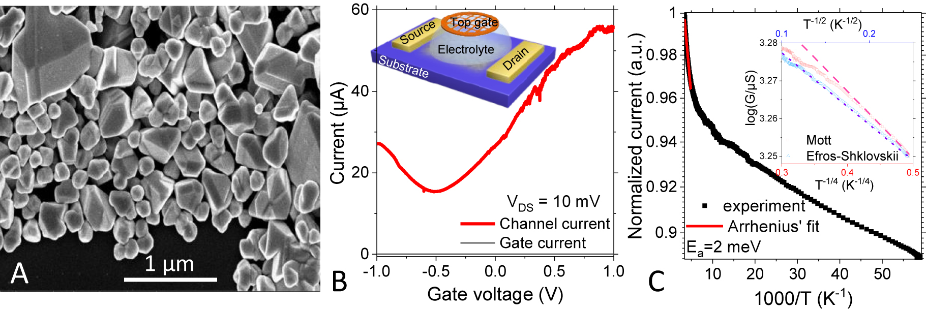
(A) Scanning electron microscopy image of large HgTe NCs. (B) Transfer curve (drain and gate current as a function of the applied gate bias) for a thin film made of large HgTe NCs used as the channel of an electrolytic transistor. Inset is a scheme of the field-effect transistor. (C) Current in logarithmic scale as a function of the temperature for a thin film made of large HgTe NCs. Arrhenius’ fit of the curve in the vicinity of room temperature leads to an activation energy of 2 meV. The inset is a plot of the log of the current as a function of T −1/2 and T −1/4.
We initially investigate the charge transport in the THz NCs. To make the material conductive we prepare a conductive ink [11, 24] in which the NCs end being capped with sulfide ions. Using this procedure, the obtained films are conductive and present an ohmic I–V curve, (see Figure S4 in Supplementary material). Upon cooling the conductance of the film slowly drops, see Figure 1C. The activation energy of the current, obtained by fitting the I–T curve close to room temperature is estimated to be 2 meV. For such quasi-metallic nanoparticles, the activation energy is mostly determined by the nanoparticle charging energy. Such low value (<k b T) for the charging energy indicates that charges in an array of large HgTe NCs behave almost as free charges. In this disordered array of NCs, the low-temperature transport is driven by variable range hopping [25, 26], whose temperature dependence gives insight into the charge delocalization [27] and bottleneck of transport. In particular, a Mott scaling (log(G) ∝ T −1/4, where G is the conductance) is expected when the density of state (availability of arrival state) is the transport bottleneck. On the other hand, when the carrier density is higher, only the Coulomb gap [26] drives the dot-to-dot transport and an Efros–Shklovskii scaling (log(G) ∝ T −1/2) is expected. Such behavior is typically the one observed in arrays of metallic nanoparticles [28]. From the inset of Figure 1C, we clearly see that the latter scaling fits better than the Mott case, confirming this quasi-metallic nature. Thus, these self-doped THz NCs contain high carrier densities up to several carriers per nanoparticle. To determine the nature of the carriers, we use a field-effect transistor configuration. As we anticipate a large carrier density in this very narrow bandgap semiconductor, we design an electrolytic transistor whose gate capacitance (≈1 μF cm−2) allows both a large tunability of the carrier density of the NCs and air operation [29]. A scheme of the device is shown in the inset of Figure 1B. We obtain an ambipolar conductance with both hole and electron conduction. The on/off ratio is low (<4) which is consistent with the expected large thermally activated carrier density, but similar to what can be obtained in graphene using electrolyte gating [30, 31].
To study the optical properties of large HgTe NCs at low frequencies, we probe the transmittance of composite films, composed by the NCs, and their surrounding environment made of dodecanethiol ligands and air, using THz TDS. We probe HgTe composite films deposited on a high-resistivity silicon substrate and use a bare high-resistivity silicon substrate as a reference sample. The THz pulse transmitted through a HgTe sample (red line) shows a temporal shift and a decrease of the electric field relative to the pulse transmitted through a reference sample (black line), as reported in Figure 2A. Applying a Fourier transform on the two recorded time-resolved electric fields, we obtain the amplitude spectra (see insert Figure 2A) and the transmittance of the composite film in the frequency domain,
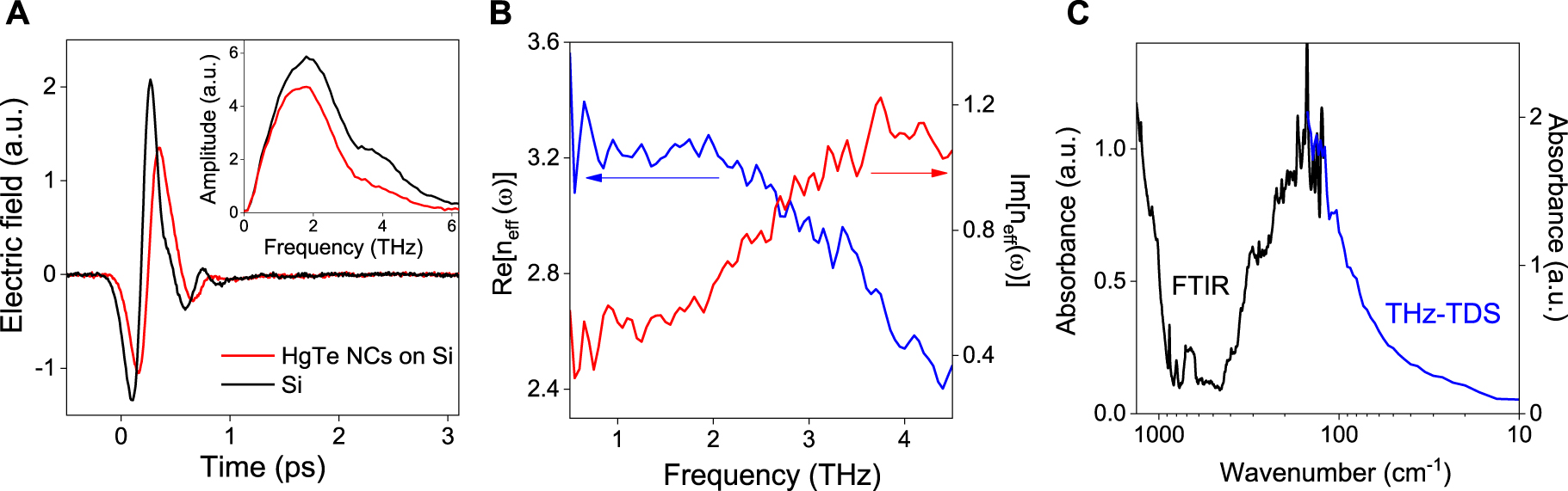
(A) The electric fields of the THz pulses transmitted through the HgTe composite film sample (red line) and through the Si substrate reference sample (black). Inset: corresponding amplitude spectra obtained by fast Fourier transform of the temporal traces. (B) The real and imaginary part of the effective index
To gain insight into the physical origin of the THz absorption resonance, we model a HgTe NC as a cubic (size L) hard-box and assume a parabolic effective mass description (m
e
* = 0.03m0). The one-electron wave functions of this model, labeled by the positive integers (n, k, l), are
where factor 2 accounts for the spin degeneracy, and we have used the fact that the electric field in the Oz direction only couple states with the same (k, l) quantum numbers. The intraband linear susceptibility of an NC,
which is the standard form of the linear susceptibility, as composed of an ensemble of Lorentzian terms weighted by the population factors
where ε
M is the relative dielectric constant of the environment of the particles and
To include in the calculation the inhomogeneous distribution of sizes of the ensemble of NCs forming the composite film, we introduce the average absorption cross-section:
Figure 3A shows the result of calculations based on the full quantum-mechanical model of the normalized absorbance of the composite film,
![Figure 3:
(A) Calculations based on the full quantum-mechanical model of the normalized absorbance of the composite film, A(ω) (red line), for a chemical potential μ = 8 meV, a broadening of γ = 10 meV, a size distribution reported in Figure S4 and experimental data obtained from THz-TDS and FTIR measurements (blue dots). (B) The absorption cross-section per unit volume of individual NCs,
C
abs
(
ω
;
L
)
/
V
NC
${C}_{\text{abs}}(\omega ;L)/{V}_{\text{NC}}$
, for NC sizes ranging from L = 1000 nm to L = 50 nm, assuming μ = 8 meV and γ = 10 meV. Inset: Peak frequency of
C
abs
(
ω
;
L
)
${C}_{\text{abs}}(\omega ;L)$
as a function of 1/L
2 in semi-log scale reflecting more quantum confinement of carriers as NCs become smaller. (C) Real,
Re
[
ϵ
(
ω
)
]
$\mathrm{Re}[{\epsilon}(\omega )]$
, and imaginary parts,
Im
[
ϵ
(
ω
)
]
$\mathrm{Im}[{\epsilon}(\omega )]$
, of the intraband permittivity as a function of the photon frequency, for a HgTe NC of size L = 92 nm, µ = 8 meV and
γ
$\gamma $
= 10 meV. For comparison, dashed curves are the real and imaginary parts of the permittivity based on classical Drude model.](/document/doi/10.1515/nanoph-2021-0249/asset/graphic/j_nanoph-2021-0249_fig_003.jpg)
(A) Calculations based on the full quantum-mechanical model of the normalized absorbance of the composite film, A(ω) (red line), for a chemical potential μ = 8 meV, a broadening of γ = 10 meV, a size distribution reported in Figure S4 and experimental data obtained from THz-TDS and FTIR measurements (blue dots). (B) The absorption cross-section per unit volume of individual NCs,
To evaluate the interplay between the quantum mechanical transitions and collective excitations, we calculate the real part,
The photoresponse of NCs at THz frequencies under optical excitation at 800 nm wavelength is now presented. For this purpose, the HgTe NC film is deposited in a z-cut quartz substrate. The silicon substrate is replaced by a quartz substrate to avoid any absorption of the optical pump light by the substrate. The incident pump fluence is 6 μJ cm−2 corresponding to a photoexcited carrier density in the range of 1016 cm−3. This difference of the THz electric field transmitted through the NCs with and without optical pumping, expressed as |ΔE(t)| = |E
ON(t) − E
OFF(t)|, is reported in Figure 4A, for a delay after the optical pump excitation of 2 ps. We observe that |ΔE(t)| shows a faster transient than the THz electric field pulse transmitted without illumination with a derivative-like temporal shape. The photoexcitation changes the electron density of the NCs and leads to a heating of the carrier distribution. Indeed, after photoexcitation at high energy (1.55 eV), the electron/hole populations are both redistributed by ultrafast intraband scattering to low energy states that are not Pauli blocked as
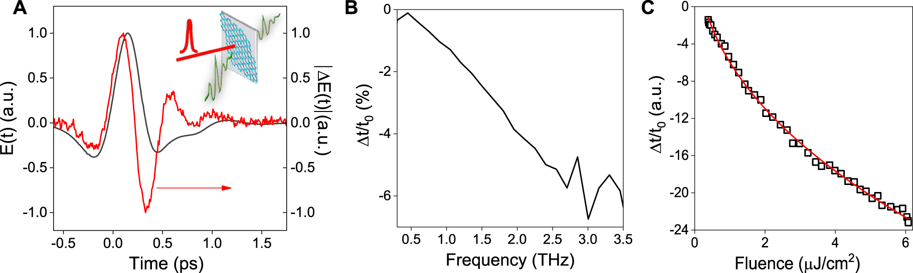
(A) The pulse transmitted through the composite HgTe film E(t) (left) and the difference of the THz electric field transmitted through the NCs with and without optical pumping, expressed as |ΔE(t)| = |E ON(t) − E OFF(t)| (right). (B) Amplitude spectrum of the pump-induced change in transmission, Δt(ω)/t 0(ω) for a delay after the optical pump excitation of 2 ps and an incident pump fluence of 6 μJ cm−2. Δt(ω) is the difference of the transmission with and without photoexcitation, Δt(ω) = t ON(ω) − t OFF(ω). (C) The peak amplitude of Δt/t 0 as a function of the incident optical pump fluence from 0.4 μJ cm−2 to 6 μJ cm−2. The red line is a fit by a square root law.
Finally, we investigate the dynamics of the observed photoinduced change in THz transmission in the HgTe NCs. Figure 5A reports −Δt/t 0 at the peak of the THz pulse as a function of the pump–probe delay time τ for a pump fluence of 6 μJ cm−2. The temporal evolution of −Δt/t 0 first rises with a characteristic time of ≈2 ps, reaches a maximum, and then decays over the next few tens of picoseconds. These observations can be explained as follows. The photocarriers are generated by the optical pump at high energies (within 100 fs). At first, the THz absorption does not change. The THz absorption only increases after the photoexcited carrier distribution cooled down to low energy states, within 1–2 ps. The photoexcited carriers are then trapped and recombine within 6 ps, where the THz absorption decreases back to its original value. The initial rise time of 2 ps is consistent with the intraband carrier–carrier and electron–optical phonon scattering in large NCs. Indeed, the weak confinement energies and high density of states in large NCs (≈100 nm diameters) lead to the efficient carrier–carrier scattering between the photoexcited carriers and the carriers in the Fermi sea, and to efficient electron–phonon coupling as even the lowest electronic states are separated by only one or two optical-phonon energies. Note that other intraband relaxation mechanisms relying on near-field energy transfer to electronic states mediated by the surface states or to molecular vibrations of the surface ligands, previously reported in strongly confined NCs of smaller sizes, are less dominant in these large NCs [40]. The decay time of −Δt/t 0 is well described by a mono-exponential decay function (red line) with a value as long as τ = 6 ps. By varying the optical pump pulse fluences from 0.08 to 0.57 μJ cm−2, the dynamics of −Δt/t 0 are still well-described by an approximatively constant relaxation time of ≈2 ps followed by a mono-exponential recombination time. Figure 5B shows that the recombination times extracted from the dynamics of −Δt/t 0 rise linearly with increasing pump fluence. We observe that the frequency dependence of Δt/t 0 is constant for all-optical pump fluences. As shown in Figure 5C, the frequency-resolved photoinduced change in transmission at different times after excitation with the pump pulse reveals that the photoinduced transmission change is progressively suppressed over the entire bandwidth of the THz probe. Importantly, the carrier recombination time of few picoseconds supports our conclusion that collective excitations are negligible since sub-picosecond decays are expected for photocarriers associated with the plasmonic absorption [23].
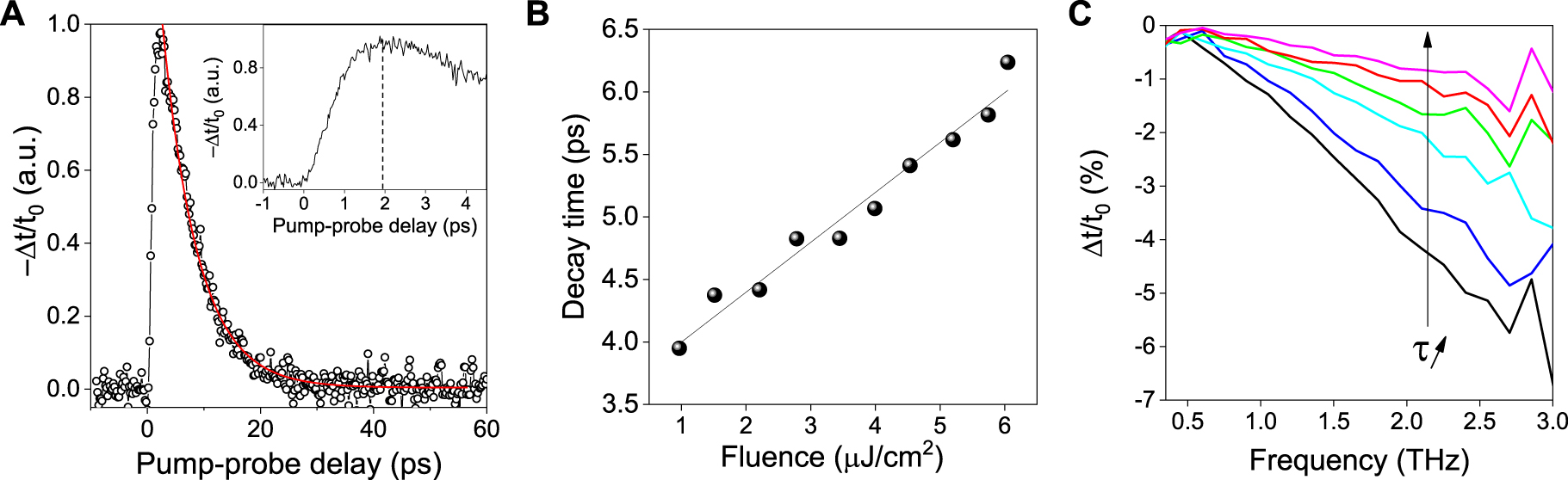
(A) The dynamics of the change of the transmission −Δt/t 0 as a function of the pump–probe delay time. (B) Decay time of −Δt/t 0 as a function of the incident optical pump fluence, showing a slow-down of the decay as the incident fluence is increased. (C) Frequency-dependent differential transmittance spectra Δt(ω)/t 0(ω) measured at different pump–probe delay times from 2 ps to 9 ps.
This raises the question of the physical mechanism responsible for these few picoseconds recombination times. Recombination pathways for hot carriers can involve Auger recombination, scattering with the optical phonon of HgTe NCs, radiative recombination, the emission of vibration modes in ligands, and trap-assisted recombination. Auger recombination processes lead to faster decay at larger incident fluence [41], which is inconsistent with our experimental observations. Moreover, interband Auger relaxation time
3 Conclusion
In conclusion, the optical properties of large self-doped HgTe NCs in the full THz spectral range were studied and showed a broad THz resonant absorption centered at ≈4.5 THz. Combining experiments with microscopic calculations, we showed that the THz absorption results from multiple intraband transitions of single carriers between quantized states and that collective excitations are negligible in self-doped THz HgTe NCs. Also, we probe the dynamics of the photo-induced transmission changes at THz frequencies and report on a relaxation time of a few picoseconds. We highlight that Auger recombination is not the main relaxation mechanism at play in this system. We attribute the main carrier recombination pathways to a resonant energy transfer from the electronic transition to the ligand vibrational modes and nonresonant nonradiative recombination channels assisted by surface traps. Our analysis of these NCs will permit to exploit large HgTe NCs for quantum engineering at THz frequencies and for the development of THz photodetectors and emitters. Further investigation will be performed to enhance the doping in large HgTe NCs to induce plasmonic effects.
4 Methods
4.1 Nanomaterials
Chemical compounds Te powder (Sigma-Aldrich, 99.99%), mercury chloride (Sigma Adrich, 99%), trioctylphosphine (TOP, Alfa aesar, 90%), dodecanethiol (DDT, Sigma Aldrich), oleic acid (Sigma-Aldrich, 90%), oleylamine (Acros, 80–90%), sodium sulfide (Sigma-Aldrich, 99.5%), dimethylformamide (DMF, VWR, 98%), lithium perchlorate (LiClO4) (Sigma-Aldrich, 98%), polyethylene glycol (PEG) (MW = 6 kg mol−1), acetone (VWR), chloroform (VWR), toluene (VWR), and ethanol absolute anhydrous (VWR). Mercury compounds are highly toxic, handle them with special care. All chemicals are used as received except oleylamine that is centrifuged before being used.
1 M TOP:Te precursor 5.08 g of Te powder are mixed in 40 mL of TOP in a three-neck flask. The flask is brought under vacuum at room temperature for 5 min and then the temperature is raised to 100 °C and degassing is further conducted over the next 20 min. The atmosphere is then switched to N2 and the temperature is raised to 275 °C. The solution is stirred until a clear orange solution is obtained. The flask is then cooled down and the color switches to yellow. At room temperature, the flask is degassed again for 10 min. Finally, this solution is transferred to an air-free glove box for storage.
NCs synthesis The following synthesis protocol is used: 18 mL of oleylamine are placed under vacuum and heated to 120 °C for 1 h. Then the solution is placed under N2 atmosphere and heated up at 300 °C. A second solution is made by mixing 0.2 mmol of HgCl2 (54 mg) and 0.2 mL of TOP:Te (1 M) in 1.8 mL of oleylamine. The solution, containing mercury and tellurium is quickly injected (within 2 min after mixing) in the hot oleylamine. The solution color quickly turns dark brown and the reaction is carried out for 3 min. 1 mL of dodecanethiol is injected at 300 °C to quench the reaction. The heating mantle is removed, the flask cooled with a flow of air. Once the temperature is around 150 °C, 9 mL of toluene are quickly added to further stop the reaction. The content of the flask is split over two tubes and ethanol is added to precipitate the NCs from the solution. The colorless supernatant is discarded and the precipitate is redispersed in 3 mL of chloroform and few drops of dodecanethiol. The NCs are washed again with 20 mL of ethanol and redispersed in 3 mL of chloroform. This process is repeated a third time.
4.2 Transport
Ligand exchange procedure To prepare thin films of nanoparticles with different capping ligands, we used a liquid phase transfer approach where the NCs end up being S2− capped [50]. To do so, we dissolved Na2S in DMF. Some NCs dissolved in hexane are mixed with this solution until a phase transfer occurs. The nonpolar supernatant is discarded before fresh hexane gets added. The polar phase is further cleaned and after decantation, the hexane is removed again. This procedure is repeated three times. Then, ethanol is added to precipitate the NCs. After centrifugation, the clear supernatant is trashed and the formed pellet redispersed in fresh DMF.
Transistor fabrication Electrodes are fabricated using standard optical lithography methods. Briefly, the surface of a Si/SiO2 (400 nm thick) wafer is cleaned by sonication in acetone. The wafer is rinsed with isopropanol and finally cleaned using O2 plasma. AZ5214 resist is spin coated and baked at 110 °C for 90 s. The substrate is exposed under UV through a pattern mask for 2 s. The film is further baked at 125 °C for 2 min to invert the resist. Then a 40 s flood exposure is performed. The resist is developed using a bath of AZ726 for 32 s, before being rinsed with pure water. We then deposit 5 nm of Cr and 80 nm of gold using a thermal evaporator. The lift-off is performed by dipping the film for 1 h in acetone. The electrodes are finally rinsed using isopropanol and dried by airflow. The electrodes are 2 mm long and spaced by 10 μm. 500 mg of LiClO4 are mixed with 2.3 g of PEG on a hot plate in a nitrogen-filled glove box at 170 °C for 2 h. Once the PEG is molten, the white Li salt can be clearly seen and slowly get dissolved. After 2 h the solution has cooled down to RT and kept in a nitrogen-filled glovebox. The solution of HgTe NCs capped with S2− and dispersed in DMF is dropcasted onto the electrodes on a hot plate at 100 °C under an N2 environment. Meanwhile, the electrolyte is softened at 100 °C. The melted electrolyte is now clear and is brushed on the colloidal quantum dots (CQD) film. A copper grid is then deposited on the top of the electrolyte and used as the top gate.
Transport measurements are conducted in air at room temperature. The sample is connected to a dual-channel Keithley 2634B which applies drain and gate voltages and measures currents. For low temperature measurements, the sample is placed on the cold finger of a close-cycle cryostat and connected to the same sourcemeter.
4.3 THz time-domain spectroscopy and Fourier transform infrared spectroscopy
The THz-TDS experiment is based on 15 fs optical pulses at a central wavelength of 800 nm delivered by a mode-locked Ti:Sa laser of 80 MHz repetition rate. A large-area interdigitated photoconductive antenna is used for THz pulse emission and a 100 µm thick GaP crystal for coherent electro-optic detection [51]. The single-cycle THz pulse emitted by the photoconductive emitter is collimated and focused on the HgTe composite film, with a spot size diameter limited by diffraction [52]. All THz optics are surrounded by an enclosure purged with dry air to minimize water vapor absorption. FTIR measurements are performed using ATR configuration. All measurements are performed at room temperature. To probe the dynamic of hot carriers at low energies in the HgTe composite film, we carry out optical pump-THz probe measurements, in which the HgTe composite film is excited by optical pump pulses at a central wavelength of 800 nm, incoming at normal incidence. The near-infrared (NIR) pump is mechanically chopped at 9 kHz and the THz probe signal is modulated via square bias applied to the photoconductive antenna at 37 kHz. The pump-induced change in the transmission of the HgTe composite film is measured using a lock-in amplifier referenced to the sum of these frequencies. The temporal resolution of the optical pump-THz probe is limited by the duration of the THz probe pulse to ≈160 fs. The NIR pump spot diameter on the HgTe composite film is ≈ 125 µm. The thickness of the composite films investigated by the THz-TDS experiment is estimated from optical microscopy to d = 13.2 µm.
For infrared spectroscopy, we use a Thermo Fischer IS 50 in an ATR configuration. In this case, the NCs solution is simply dried on the diamond cell. A Globar source equivalent to a 700 °C blackbody is used as a/the source, the beam splitter is made of an XT-KBr beamsplitter for mid infrared (7500–400 cm−1 range) and using a Si beam splitter for the far infrared (2000–150 cm−1 range). The detector is a deuterated triglycine sulfate (DTGS) detector. Each spectrum is acquired with a 4 cm−1 resolution and average of 32 times.
Funding source: H2020 European Research Council 10.13039/501100000781
Award Identifier / Grant number: ERC consolidator grant no. 820133
Award Identifier / Grant number: ERC starting grant no.756225
Funding source: Agence Nationale de la Recherche 10.13039/501100001665
Award Identifier / Grant number: ANR-11-IDEX-0004-02
Award Identifier / Grant number: ANR-18CE30-0023-01
Award Identifier / Grant number: ANR-19-CE09-0017
Award Identifier / Grant number: ANR-19-CE09-0026
Award Identifier / Grant number: ANR-19-CE24-0022
Award Identifier / Grant number: ANR-20-ASTR-0008-01
Acknowledgments
The authors thank Ricardo Lobo for assistance with Fourier transform infrared spectroscopy measurements. The project is supported by ERC starting grant blackQD (grant n° 756225) and consolidator grant LEON (grant n° 820133). We acknowledge the use of clean-room facilities from the “Centrale de Proximité Paris-Center”. This work has been supported by the Region Ile-de-France in the framework of DIM Nano-K (grant dopQD). This work was supported by French state funds managed by the ANR within the Investissements d'Avenir program by Labex Matisse (ANR-11-IDEX-0004-02), and also by the grant FRONTAL (ANR-19-CE09-0017), IPER-Nano2 (ANR-18CE30-0023-01), Copin (ANR-19-CE24-0022), Graskop (ANR-19-CE09-0026), and NITQuantum (ANR-20-ASTR-0008-01).
-
Author contribution: All the authors have accepted responsibility for the entire content of this submitted manuscript and approved submission.
-
Research funding: This research was funded by ERC starting grant blackQD (grant n° 756225), consolidator grant LEON (grant n° 820133), Region Ile-de-France in the framework of DIM Nano-K (grant dopQD), Labex Matisse (ANR-11-IDEX-0004-02), FRONTAL (ANR-19-CE09-0017), IPER-Nano2 (ANR-18CE30-0023-01), Copin (ANR-19-CE24-0022), Graskop (ANR-19-CE09-0026) and NITQuantum (ANR-20-ASTR-0008-01).
-
Conflict of interest statement: The authors declare no conflicts of interest regarding this article.
References
[1] C. Gréboval, A. Chu, N. Goubet, C. Livache, S. Ithurria, and E. Lhuillier, “Mercury chalcogenide quantum dots: material perspective for device integration,” Chem. Rev., vol. 121, pp. 3627–3700, 2021. https://doi.org/10.1021/acs.chemrev.0c01120.Suche in Google Scholar
[2] E. Lhuillier and P. Guyot-Sionnest, “Recent progresses in mid infrared nanocrystal optoelectronics,” IEEE J. Sel. Top. Quant. Electron., vol. 23, 2017, Art no. 6000208. https://doi.org/10.1109/jstqe.2017.2690838.Suche in Google Scholar
[3] A. Svane, N. E. Christensen, M. Cardona, A. N. Chantis, M. van Schilfgaarde, and T. Kotani, “Quasiparticle band structures of β-HgS, HgSe, and HgTe,” Phys. Rev. B, vol. 84, 2011, Art no. 205205. https://doi.org/10.1103/physrevb.84.205205.Suche in Google Scholar
[4] J. M. Pietryga, R. D. Schaller, D. Werder, M. H. Stewart, V. I. Klimov, and J. A. Hollingsworth, “Pushing the band gap envelope: mid-infrared emitting colloidal PbSe quantum dots,” J. Am. Chem. Soc., vol. 126, pp. 11752–11753, 2004. https://doi.org/10.1021/ja047659f.Suche in Google Scholar
[5] A. Rogach, S. V. Kershaw, M. Burt, et al., “Colloidally prepared HgTe nanocrystals with strong room-temperature infrared luminescence,” Adv. Mater., vol. 11, pp. 552–555, 1999. https://doi.org/10.1002/(sici)1521-4095(199905)11:7<552::aid-adma552>3.0.co;2-q.10.1002/(SICI)1521-4095(199905)11:7<552::AID-ADMA552>3.0.CO;2-QSuche in Google Scholar
[6] M. V. Kovalenko, E. Kaufmann, Pachinger, et al.., “Colloidal HgTe nanocrystals with widely tunable narrow band gap Energies: from telecommunications to molecular vibrations,” J. Am. Chem. Soc., vol. 128, pp. 3516–3517, 2006. https://doi.org/10.1021/ja058440j.Suche in Google Scholar
[7] S. Keuleyan, E. Lhuillier, V. Brajuskovic, and P. Guyot-Sionnest, “Mid-infrared HgTe colloidal quantum dot photodetectors,” Nat. Photonics, vol. 5, pp. 489–493, 2011. https://doi.org/10.1038/nphoton.2011.142.Suche in Google Scholar
[8] S. E. Keuleyan, P. Guyot-Sionnest, C. Delerue, and G. Allan, “Mercury telluride colloidal quantum dots: electronic structure, size-dependent spectra, and photocurrent detection up to 12 µm,” ACS Nano, vol. 8, pp. 8676–8682, 2014. https://doi.org/10.1021/nn503805h.Suche in Google Scholar
[9] N. Goubet, A. Jagtap, C. Livache, et al.., “Terahertz HgTe nanocrystals: beyond confinement,” J. Am. Chem. Soc., vol. 140, pp. 5033–5036, 2018. https://doi.org/10.1021/jacs.8b02039.Suche in Google Scholar
[10] V. Rinnerbauer, K. Hingerl, M. Kovalenko, and W. Heiss, “Effect of quantum confinement on higher transitions in HgTe nanocrystals,” Appl. Phys. Lett., vol. 89, 2006, Art no. 193114. https://doi.org/10.1063/1.2387110.Suche in Google Scholar
[11] B. Martinez, J. Ramade, C. Livache, et al., “HgTe nanocrystal inks for extended short‐wave infrared detection,” Adv. Opt. Mater., vol. 7, 2019, Art no. 1900348. https://doi.org/10.1002/adom.201900348.Suche in Google Scholar
[12] A. Chu, B. Martinez, S. Ferré, et al.., “HgTe nanocrystals for SWIR detection and their integration up to the focal plane array,” ACS Appl. Mater. Interfaces, vol. 11, pp. 33116–33123, 2019. https://doi.org/10.1021/acsami.9b09954.Suche in Google Scholar PubMed
[13] X. Tang, M. M. Ackerman, M. Chen, and P. Guyot-Sionnest, “Dual-band infrared imaging using stacked colloidal quantum dot photodiodes,” Nat. Photonics, vol. 13, pp. 277–282, 2019. https://doi.org/10.1038/s41566-019-0362-1.Suche in Google Scholar
[14] M. H. Hudson, M. Chen, V. Kamysbayev, et al.., “Conduction band fine structure in colloidal HgTe quantum dots,” ACS Nano, vol. 12, pp. 9397–9404, 2018. https://doi.org/10.1021/acsnano.8b04539.Suche in Google Scholar PubMed
[15] E. Lhuillier, M. Scarafagio, P. Hease, et al.., “Infrared photodetection based on colloidal quantum-dot films with high mobility and optical absorption up to THz,” Nano Lett., vol. 16, pp. 1282–1286, 2016. https://doi.org/10.1021/acs.nanolett.5b04616.Suche in Google Scholar PubMed
[16] A. Jagtap, C. Livache, B. Martinez, et al.., “Emergence of intraband transitions in colloidal nanocrystals,” Opt. Mater. Express, vol. 8, p. 1174, 2018. https://doi.org/10.1364/ome.8.001174.Suche in Google Scholar
[17] K. S. Jeong, Z. Deng, S. Keuleyan, H. Liu, and P. Guyot-Sionnest, “Air-stable n-doped colloidal HgS quantum dots,” J. Phys. Chem. Lett., vol. 5, pp. 1139–1143, 2014. https://doi.org/10.1021/jz500436x.Suche in Google Scholar PubMed
[18] J. Kim, D. Choi and K. S. Jeong, “Self-doped colloidal semiconductor nanocrystals with intraband transitions in steady state,” Chem. Commun., vol. 54, pp. 8435–8445, 2018. https://doi.org/10.1039/c8cc02488j.Suche in Google Scholar PubMed
[19] I. Ramiro, O. Özdemir, S. Christodoulou, et al.., “Mid- and long-wave infrared optoelectronics via intraband transitions in PbS colloidal quantum dots,” Nano Lett., vol. 20, pp. 1003–1008, 2020. https://doi.org/10.1021/acs.nanolett.9b04130.Suche in Google Scholar PubMed PubMed Central
[20] B. Martinez, C. Livache, L. D. Notemgnou Mouafo, et al.., “HgSe self-doped nanocrystals as a platform to investigate the effects of vanishing confinement,” ACS Appl. Mater. Interfaces, vol. 9, pp. 36173–36180, 2017. https://doi.org/10.1021/acsami.7b10665.Suche in Google Scholar PubMed
[21] N. Goubet, C. Livache, B. Martinez, et al.., “Wave-function engineering in HgSe/HgTe colloidal heterostructures to enhance mid-infrared photoconductive properties,” Nano Lett., vol. 18, pp. 4590–4597, 2018. https://doi.org/10.1021/acs.nanolett.8b01861.Suche in Google Scholar PubMed
[22] P. Guyot-Sionnest, B. Wehrenberg, and D. Yu, “Intraband relaxation in CdSe nanocrystals and the strong influence of the surface ligands,” J. Chem. Phys., vol. 123, 2005, Art no. 074709. https://doi.org/10.1063/1.2004818.Suche in Google Scholar PubMed
[23] J. Qu, C. Livache, B. Martinez, et al.., “Transport in ITO nanocrystals with short- to long-wave infrared absorption for heavy-metal-free infrared photodetection,” ACS Appl. Nano Mater., vol. 2, pp. 1621–1630, 2019. https://doi.org/10.1021/acsanm.9b00067.Suche in Google Scholar
[24] M. Chen, X. Lan, X. Tang, et al.., “High carrier mobility in HgTe quantum dot solids improves mid-IR photodetectors,” ACS Photonics, vol. 6, pp. 2358–2365, 2019. https://doi.org/10.1021/acsphotonics.9b01050.Suche in Google Scholar
[25] H. Liu, A. Pourret, and P. Guyot-Sionnest, “Mott and Efros-Shklovskii variable range hopping in CdSe quantum dots films,” ACS Nano, vol. 4, pp. 5211–5216, 2010. https://doi.org/10.1021/nn101376u.Suche in Google Scholar PubMed
[26] A. L. Efros and B. I. Shklovskii, “Coulomb gap and low temperature conductivity of disordered systems,” J. Phys. C Solid State Phys., vol. 8, pp. L49–L51, 1975. https://doi.org/10.1088/0022-3719/8/4/003.Suche in Google Scholar
[27] T. Chen, K. V. Reich, N. J. Kramer, H. Fu, U. R. Kortshagen, and B. I. Shklovskii, “Metal-insulator transition in films of doped semiconductor nanocrystals,” Nat. Mater., vol. 15, pp. 299–303, 2016. https://doi.org/10.1038/nmat4486.Suche in Google Scholar PubMed
[28] H. Moreira, Q. Yu, B. Nadal, et al.., “Electron cotunneling transport in gold nanocrystal arrays,” Phys. Rev. Lett., vol. 107, 2011, Art no. 176803. https://doi.org/10.1103/physrevlett.107.176803.Suche in Google Scholar PubMed
[29] E. Lhuillier, S. Ithurria, A. Descamps-Mandine, et al.., “Investigating the n- and p-type electrolytic charging of colloidal nanoplatelets,” J. Phys. Chem. C, vol. 119, pp. 21795–21799, 2015. https://doi.org/10.1021/acs.jpcc.5b05296.Suche in Google Scholar
[30] W. Fu, L. Feng, G. Panaitov, et al.., “Biosensing near the neutrality point of graphene,” Sci. Adv., vol. 3, 2017, Art no. e1701247. https://doi.org/10.1126/sciadv.1701247.Suche in Google Scholar PubMed PubMed Central
[31] A. Robin, E. Lhuillier, X. Z. Xu, et al.., “Engineering the charge transfer in all 2D graphene-nanoplatelets heterostructure photodetectors,” Sci. Rep., vol. 6, p. 24909, 2016. https://doi.org/10.1038/srep24909.Suche in Google Scholar PubMed PubMed Central
[32] W. Szuszkiewicz, A. M. Witowski, and M. Grynberg Phys. Status Solidi B, vol. 87, pp. 637–645, 1978. https://doi.org/10.1002/pssb.2220870229.Suche in Google Scholar
[33] P. Rastogi, A. Chu, T. H. Dang, et al.., “Complex optical index of HgTe nanocrystal infrared thin films and its use for short wave infrared photodiode design,” Adv. Opt. Mater., vol. 9, 2021, Art no. 2002066. https://doi.org/10.1002/adom.202002066.Suche in Google Scholar
[34] K. Prashant, “Jain, plasmon-in-a-box: on the physical nature of few-carrier plasmon resonances,” J. Phys. Chem. Lett., vol. 5, p. 3112, 2014. https://doi.org/10.1021/jz501456t.Suche in Google Scholar PubMed
[35] X. Fan, W. Zheng, and D. Singh, “Light scattering and surface plasmons on small spherical particles,” Light Sci. Appl., vol. 3, p. e179, 2014. https://doi.org/10.1038/lsa.2014.60.Suche in Google Scholar
[36] H.-K. Nienhuys and V. Sundström, “Influence of plasmons on terahertz conductivity measurements,” Appl. Phys. Lett., vol. 87, 2005, Art no. 012101. https://doi.org/10.1063/1.1977213.Suche in Google Scholar
[37] J. Luther, P. Jain, T. Ewers, and A. P. Alivisatos, “Localized surface plasmon resonances arising from free carriers in doped quantum dots,” Nat. Mater., vol. 10, p. 361, 2011. https://doi.org/10.1038/nmat3004.Suche in Google Scholar PubMed
[38] K. Prashant, “Jain, plasmon-in-a-box: on the physical nature of few-carrier plasmon resonances,” J. Phys. Chem. Lett., vol. 5, p. 3112, 2014. https://doi.org/10.1021/jz501456t.Suche in Google Scholar
[39] A. M. Schimpf, N. Thakkar, C. E. Gunthardt, D. J. Masiello, and D. R. Gamelin, “Charge-tunable quantum plasmons in colloidal semiconductor nanocrystals,” ACS Nano, vol. 8, p. 1065, 2014. https://doi.org/10.1021/nn406126u.Suche in Google Scholar PubMed
[40] P. Guyot-Sionnest, B. Wehrenberg, and D. Yu, “Intraband relaxation in CdSe nanocrystals and the strong influence of the surface ligands,” J. Chem. Phys., vol. 123, 2005, Art no. 074709. https://doi.org/10.1063/1.2004818.Suche in Google Scholar PubMed
[41] J. Lim, Y. C. Choi, D. Choi, et al., “Ultrafast intraband Auger process in self-doped colloidal quantum dots,” Matter, vol. 4, pp. 1072–1086, 2021. https://doi.org/10.1016/j.matt.2020.12.026.Suche in Google Scholar
[42] C. Melnychuk and P. Guyot-Sionnest, “Auger suppression in n-type HgSe colloidal quantum dots,” ACS Nano, vol. 13, pp. 10512–10519, 2019. https://doi.org/10.1021/acsnano.9b04608.Suche in Google Scholar PubMed
[43] C. Melnychuk and P. Guyot-Sionnest, “Slow auger relaxation in HgTe colloidal quantum dots,” J. Phys. Chem. Lett., vol. 9, pp. 2208–2211, 2018. https://doi.org/10.1021/acs.jpclett.8b00750.Suche in Google Scholar PubMed
[44] J. Qu, P. Rastogi, C. Gréboval, et al.., “Electroluminescence from HgTe nanocrystals and its use for active imaging,” Nano Lett., vol. 20, no. 8, pp. 6185–6190, 2020. https://doi.org/10.1021/acs.nanolett.0c02557.Suche in Google Scholar PubMed
[45] S. Keuleyan, J. Kohler, and P. Guyot-Sionnest, “Photoluminescence of mid-infrared HgTe colloidal quantum dots,” J. Phys. Chem. C, vol. 118, pp. 2749–2753, 2014. https://doi.org/10.1021/jp409061g.Suche in Google Scholar
[46] P. Geiregat, A. J. Houtepen, L. K. Sagar, et al.., “Continuous-wave infrared optical gain and amplified spontaneous emission at ultralow threshold by colloidal HgTe quantum dots,” Nat. Mater., vol. 17, pp. 35–42, 2018. https://doi.org/10.1038/nmat5000.Suche in Google Scholar PubMed
[47] N. M. Abdelazim, Q. Zhu, Y. Xiong, et al.., “Room temperature synthesis of HgTe quantum dots in an aprotic solvent realizing high photoluminescence quantum yields in the infrared,” Chem. Mater., vol. 29, pp. 7859–7867, 2017. https://doi.org/10.1021/acs.chemmater.7b02637.Suche in Google Scholar
[48] C. T. Smith, M. A. Leontiadou, R. Page, P. O'Brien, and D. J. Binks, “Ultrafast charge dynamics in trap‐free and surface‐trapping colloidal quantum dots,” Adv. Sci., vol. 2, 2015, Art no. 1500088. https://doi.org/10.1002/advs.201500088.Suche in Google Scholar PubMed PubMed Central
[49] Q. Wen, S. V. Kershaw, S. Kalytchuk, et al.., “Impact of D2O/H2O solvent exchange on the emission of HgTe and CdTe quantum dots: polaron and energy transfer effects,” ACS Nano, vol. 10, pp. 4301–4311, 2016. https://doi.org/10.1021/acsnano.5b07852.Suche in Google Scholar PubMed
[50] A. Nag, M. V. Kovalenko, J.-S. Lee, W. Liu, B. Spokoyny, and D. V. Talapin, “Metal-free inorganic ligands for colloidal nanocrystals: S2–, HS–, Se2–, HSe–, Te2–, HTe–, TeS32–, OH–, and NH2– as surface ligands,” J. Am. Chem. Soc., vol. 133, pp. 10612–10620, 2011. https://doi.org/10.1021/ja2029415.Suche in Google Scholar PubMed
[51] J. Madéo, N. Jukam, D. Oustinov, et al., “Frequency tunable terahertz interdigitated photoconductive antennas,” Electron. Lett., vol. 46, pp. 611–613, 2010.10.1049/el.2010.0440Suche in Google Scholar
[52] M. Baillergeau, K. Maussang, T. Nirrengarten, et al.., “Diffraction-limited ultrabroadband terahertz spectroscopy,” Sci. Rep., vol. 6, p. 24811, 2016. https://doi.org/10.1038/srep24811.Suche in Google Scholar PubMed PubMed Central
Supplementary Material
The online version of this article offers supplementary material (https://doi.org/10.1515/nanoph-2021-0249).
© 2021 Thibault Apretna et al., published by De Gruyter, Berlin/Boston
This work is licensed under the Creative Commons Attribution 4.0 International License.
Artikel in diesem Heft
- Frontmatter
- Reviews
- The potential of SERS as an AST methodology in clinical settings
- Mesoscopic electrodynamics at metal surfaces
- Research Articles
- Broadband and ultrafast all-optical switching based on transition metal carbide
- Black phosphorus nanosheets and paclitaxel encapsulated hydrogel for synergistic photothermal-chemotherapy
- Magnetic plasmons induced in a dielectric-metal heterostructure by optical magnetism
- Single-shot imaging of surface molecular ionization in nanosystems
- Tunable nonlinear optical responses of few-layer graphene through lithium intercalation
- Heterostructured CuO@ZnO@Ag biomimetic setaria as wettability-switchable difunctional SERS substrate for trace pesticide and DNA detections
- Perfect metamaterial absorber improved laser-driven flyer
- Twist angle dependent absorption feature induced by interlayer rotations in CVD bilayer graphene
- Lab on optical fiber: surface nano-functionalization for real-time monitoring of VOC adsorption/desorption in metal-organic frameworks
- Local field effects in ultrafast light–matter interaction measured by pump-probe spectroscopy of monolayer MoSe2
- Microsphere-assisted manipulation of a single Ag nanowire
- Polarization-dependent mode coupling in hyperbolic nanospheres
- Few picosecond dynamics of intraband transitions in THz HgTe nanocrystals