Harmonic generation with multi-layer dielectric metasurfaces
-
Giuseppe Marino

 ,
Davide Rocco
,
Carlo Gigli
,
Grégoire Beaudoin
,
Davide Rocco
,
Carlo Gigli
,
Grégoire Beaudoin

Abstract
Metasurfaces have recently gained extensive interest because of their extraordinary optical behavior as artificial material interfaces with ultrahigh compactness. In this framework, dielectric platforms have newly become very promising for nonlinear nanophotonics, providing opportunities, especially for ultrafast optical switching, and high harmonic generation, opening the research field of nonlinear metaoptics. Up to now, nonlinear metaoptics have been mostly explored using single metasurfaces. However, in a long-term vision, the stacking of optical metasurfaces, very challenging in terms of fabrication, is one key goal of this research field. Here, we demonstrate a three-layer metasurface in the AlGaAs-on-insulator platform, which improves the second harmonic generation efficiency by more than one order of magnitude with respect to its one-layer counterpart. Our achievement paves the way toward phase-shaping multilayer and multifunctional all-dielectric metasurfaces.
1 Introduction
Photonics at the micro- and nano-scale has experienced a spectacular development in the last two decades, thanks to technological progress and capability of manipulating near and far fields of radiating nanoparticles. Plasmonic and high-contrast dielectric meta-atoms arranged in an ordered array, in two or three dimensions, have shown their potential for shaping nonlinear optical effects at the nanoscale [1], [2], [3], [4], [5], [6], [7], [8].
Harmonic generation and wavefront shaping can occur in all-dielectric open Mie resonators, depending on their nonlinear and scattering properties, as light at the fundamental frequency (FF) is coupled to their displacement currents. To this end, the resonator should have a characteristic size L and a refractive index n such that
Historically, the first nonlinear nanoresonator of this type was made of silicon and resulted in third-harmonic generation (THG) with two-order-of-magnitude higher efficiency than in bulk silicon [5]. To increase such efficiency, nanoresonators with multi-mode interference in the form of Fano resonances [9], [10], nonradiative anapole [11] or bound states in the continuum [12], [13] have been proposed. Moreover, a feedback mechanism provided by a gold mirror has been used to boost THG pumped at the anapole condition [14]. However, bulk silicon only exhibits relatively weak cubic nonlinearity and is affected by two-photon absorption at telecom wavelength, which limits the maximum FF power. Higher conversion efficiencies have been achieved with quadratic nonlinearity in noncentrosymmetric III-V semiconductors such as GaP [6], GaAs [15], and AlGaAs [7], [8], where resonators with low-quality factor (Q) have enabled second harmonic generation (SHG) efficiency
The special case of nonlinear metasurfaces and 2D nonlinear metamaterials, where the electromagnetic features are further engineered by the ordered structure of nonlinear meta-atoms, have attracted a great interest in the scientific community in the quest for molding the properties of light beyond what was previously possible [1, 17–20]. Their planar profiles make them particularly appealing, because of a simpler fabrication process than 3D metasurfaces and metamaterials and the long-sought promise for integration with on-chip nanophotonic devices [21], [22].
Different metasurfaces have already been demonstrated for several optical operations (lenses, imaging, harmonic generation, just to mention a few) [23], [24], and the natural question of how to design and engineer layered systems with stacked metasurfaces has been raised only recently [25], [26], [27], [28]. The research field is promising and potentially huge, with the long-term vision of multi-layer systems able to perform complex optical transformations by combining linear, nonlinear, passive, and active metasurfaces into a single device. However, this problem is very challenging, not only from the fabrication viewpoint but also for modeling, as full-wave simulations become easily too cumbersome for device engineering [29]. Apart from simple cases where the metasurface is placed in front of a reflector, to date, the issue has only been addressed in the linear regime [25], [26], [27], [28].
Recently, we demonstrated that a periodic structure of Mie resonators can achieve the independent control of the second harmonic (SH) radiation diagram and polarization [30], [31]. In those works, we defined an effective metasurface polarizability accounting for the perturbation of resonances from the isolated constituents, because of in-plane Bragg scattering. By engineering this polarizability, we were able to excite higher-Q resonances, whereas both preserving the polarization properties of single Mie-resonators and achieving SHG in the zero-diffracted order. Here, for the first time to our knowledge, we demonstrate a multi-layer semiconductor metasurface to perform SHG. Our specific answer to the problem of low conversion efficiency, which is currently at the forefront of research in nonlinear nanophotonics, is a three-layer stack (i.e., an optical triplet) in the AlGaAs platform, as illustrated in Figure 1. In such a system, the combination of three metasurfaces is experimentally demonstrated to increase SH frequency bandwidth and power conversion efficiencies. The multi-functional behavior of our triplet by means of beam shaping is also confirmed by the zero-order diffraction measured at the SH, resulting from the combination of the meta-atoms radiation and a 3D nonuniform array factor.
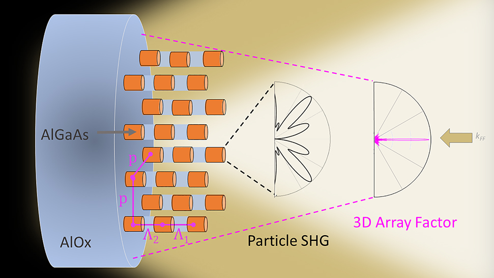
Schematic of a three-layer metasurface (Λ1 and Λ2 apart from each other) with SH emission pattern decomposed in SHG from the single nanoresonator (dark line) and array factor radiation from the 3D array with in-plane periodicity p (pink line).
Our results demonstrate properties which are very promising for a variety of applications, including nonlinear spectroscopy [32], [33], high lateral resolution imaging [34], photodynamic therapy [35], and photocatalysis [36].
The rest of this Letter is organized as follows: Sections 2 and 3 describe the design and fabrication of the three-layer nonlinear metasurface, respectively; in Section 4, measurements of SH frequency bandwidth and power efficiency of our triplet are reported and compared with 3D theoretical simulations.
2 Design
To achieve a feedback mechanism at the FF in the vertical direction, we piled up three layers of the nonlinear AlGaAs metasurface reported in [30], separated by layers of a low-index material, whose thickness is designed so as to maximize the FF internal energy in each meta-atom. The internal energy, E
int, is calculated as
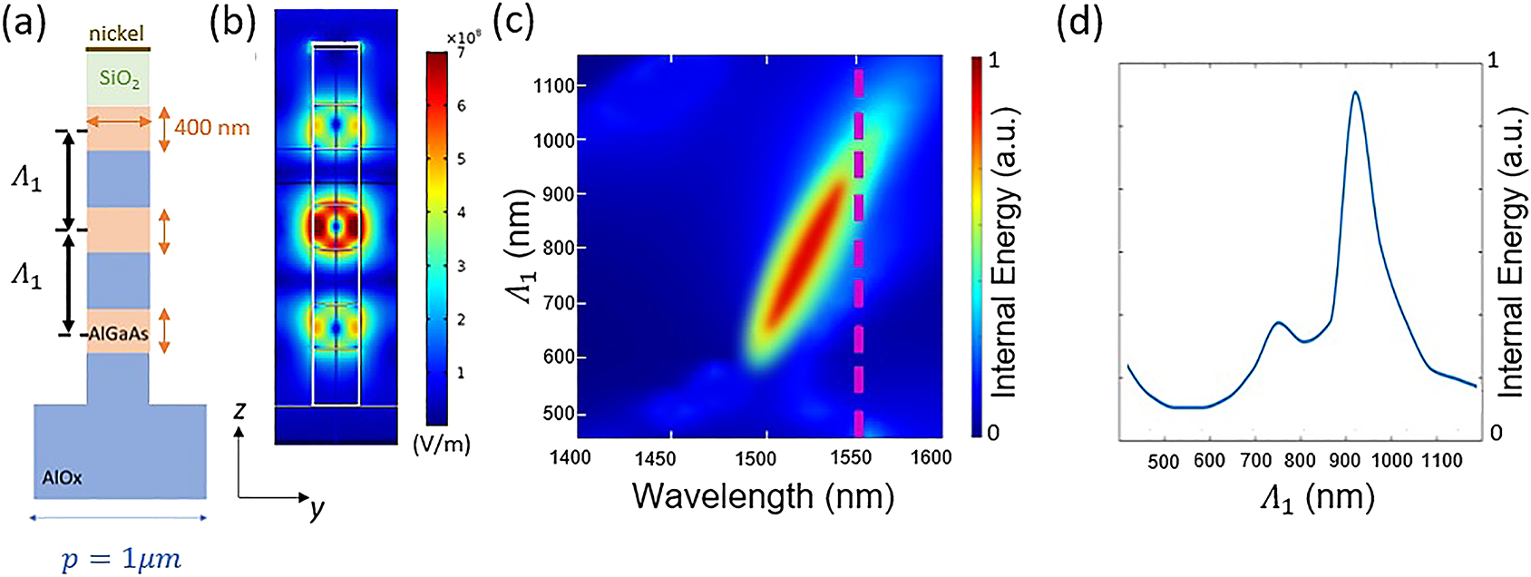
(a) Sketch of the proposed unitary cell with vertical spacing Λ1 = 900 nm and in-plane period p = 1 μm. Note that for the sake of coherence with the fabricated structure, the simulation includes additional cylinders of SiO2 and nickel on the top and of AlOx at the bottom, even though they are optically inactive (see Section S1 of the Supplementary Material) (b) Electric-field distribution for the triplet metasurfaces in (a). The pump is a y-polarized plane wave with 1 GW/cm2 intensity. (c) Internal energy inside the AlGaAs nanodisks vs. incident FF wavelength. (d) Internal energy vs. Λ1, for a pump wavelength λ = 1550 nm.
3 Fabrication
The metasurface triplet (see Figure 3) consists of three Al0.18Ga0.82As layers (orange regions in Figures 2a and 3a) separated by a low-index oxide spacer (AlOx, n = 1.6), with the whole stack lying on an optical substrate of AlOx (blue layers in Figures 2a and 3a). Following the technique that was established for single-layer metasurfaces [22], the epitaxial structure is grown by MOCVD on a (100)-GaAs wafer. It includes three Al0.98Ga0.02As layers to be selectively oxidized at a later stage (bottom layer of 1 µm and two upper layers of 500 nm), alternated with three Al0.18Ga0.82As layers to provide optical confinement. At each
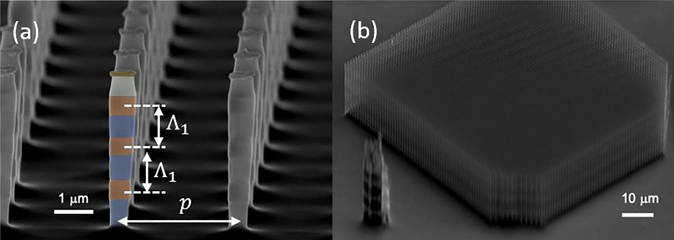
(a) Scanning Electron Microscope (SEM) image of three lines of a three-layer metasurface with
4 Results and discussions
The SHG from the three-layer metasurface is measured via a customized nonlinear microscope pumped with a 160 fs pulse, 1 MHz repetition rate, and
Figure 4a shows both numerical and measured SHG from the three-layer metasurface as a function of the pillar radius, for a fixed in-plane period p = 1.1 μm. Our numerical predictions are made for two different configurations: 1) three-layer metasurfaces made of identical pillars with nominal radius r (solid blue line); 2) three-layer metasurfaces made of pillars with distributed radii (dashed blue line), according to fabrication constraints (from top to bottom radii are: r + 10 nm, r − 10 nm, r − 30 nm, see Figure S3 in Supplementary Material). We numerically estimate an SHG efficiency almost equal to
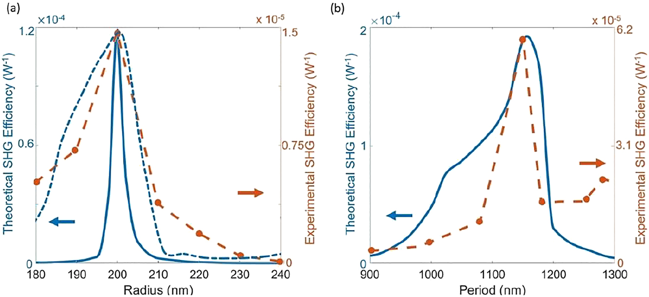
(a) Calculated three-layer metasurfaces with identical pillar radii r (blue solid curve), three-layer metasurfaces with distributed pillar radii r + 10 nm, r − 10 nm, r − 30 nm (blue dashed curve), and experimental (orange line) SHG efficiency vs. nanodisks radius, for p = 1100 nm, (b) Calculated (blue curve) and experimental (orange line) SHG efficiency vs. p for a pillar radius r = 200 nm. A negative shift of about 80 nm in the experimental period is added in the figure.
Figure 4b reports the SHG efficiency as a function of the metasurface period, for a fixed radius of 200 nm. Again, the maximum numerical estimation (blue line) of SHG efficiency is of the order of
Moreover, we have investigated the SHG radiation pattern of the three-layer metasurfaces. The peculiar spatial frequency selectivity, reported in Figure S3 of the Supplementary Material, recalls the zero-order diffraction already demonstrated for the single metasurface [30]. However, at variance with the latter, here the far-field SHG results from the contribution of the single-particle SH radiation and the 3D array factor, giving rise to more than one order of magnitude (15×) enhanced emission power, as aforementioned. Further design of these two parameters, out of the scope of this work, could result in fine beam shaping and improve the multi-functional behavior of the three-layer metasurfaces.
Finally, to disentangle the contribution of the vertical confinement from the in-plane Bragg scattering we have also investigated isolated three-layer nanoresonators, whose fabricated structure is imaged in Figure 3a. Experimentally, a diffraction-limited spot with a 2.4 µm waist was applied via a high-NA (=0.8) objective in the aforementioned microscopy working in reflection geometry. Figure 5a shows the typical two lobes expected from the isolated structure [40] with a maximum peak at around 45° from the normal, confirming that Mie-resonances involved in the SHG process are not affected by the vertical confinement. More importantly, looking at the normalized SHG efficiency as a function of the radius reported in Figure 5b (orange dashed line), the maximum value of
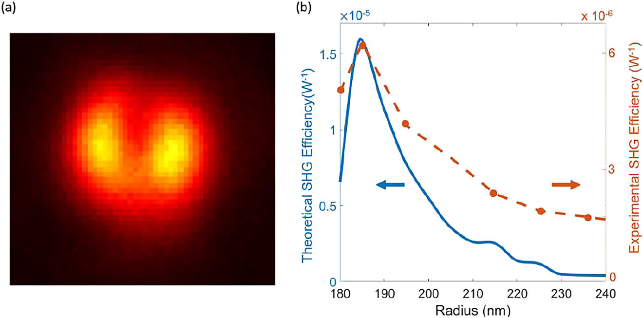
(a) Microscope image of SHG from in-plane isolated nano-resonator in the multilayer structure with radius equal to 185 nm. (b) Measured (orange curve) and calculated (blue curve) SHG efficiency from (a) as a function of radius.
5 Conclusion
We have designed, fabricated, and characterized a three-layer metasurface in AlGaAs platforms, proving the feasibility of enhanced SH generation. With respect to one-layer metasurface, we predict and measure more than one-order-of-magnitude (15×) enhanced SHG efficiencies. Beyond harmonic efficiency, the multi-functional behavior of the three-layer metasurfaces is proved by maintaining a high SH signal for different triplet radii. Our results pave the way to a multifunctional nonlinear platform via multi-layer all-dielectric metasurfaces.
Funding source: Ministero dell’Istruzione, dell’Università e della Ricerca
Award Identifier / Grant number: NOMEN (2017MP7F8F)
Funding source: RENATECH
Funding source: National Research Council Joint Laboratories
Award Identifier / Grant number: SAC.AD002.026 (OMEN)
Funding source: Agence Nationale de la Recherche
Award Identifier / Grant number: ANR-18-CE92-0043
Acknowledgments
The authors thank Félix Garreau De Loubresse and Amir Loucif for nanofabrication.
-
Author contributions: All the authors have accepted responsibility for the entire content of this submitted manuscript and approved submission.
-
Research funding: G.L. acknowledges financial support by ANR through the NANOPAIR project (ANR-18-CE92-0043). C.D.A. and G.L. acknowledge the National Research Council Joint Laboratories program, project SAC.AD002.026 (OMEN). CDA acknowledges the Italian Ministry of University and Research (MIUR) through the PRIN project NOMEN (2017MP7F8F). I.S. acknowledges the french RENATECH network.
-
Conflict of interest statement: The authors declare no conflicts of interest regarding this article.
References
[1] B. Wells, A. Y. Bykov, G. Marino, M. E. Nasir, A. V. Zayats, and V. A. Podolskiy, “Structural second-order nonlinearity in plasmonic metamaterials,” Optica, vol. 5, no. 12, pp. 1502–1507, 2018, https://doi.org/10.1364/optica.5.001502.Search in Google Scholar
[2] B. Corcoran, C. Monat, C. Grillet, et al.., “Green light emission in silicon through slow-light enhanced third-harmonic generation in photonic-crystal waveguides,” Nat. Photonics, vol. 3, no. 4, p. 206, 2009, https://doi.org/10.1038/nphoton.2009.28.Search in Google Scholar
[3] S. O. Yurchenko, K. I. Zaytsev, E. A. Gorbunov, et al.., “Enhanced third-harmonic generation in photonic crystals at band-gap pumping,” J. Phys. Appl. Phys., vol. 50, no. 5, p. 055105, 2017, https://doi.org/10.1088/1361-6463/aa53d4.Search in Google Scholar
[4] J. D. Joannopoulos, P. R. Villeneuve, and S. Fan, “Photonic crystals,” Solid State Commun., vol. 102, nos 2-3, pp. 165–173, 1997, https://doi.org/10.1016/s0038-1098(96)00716-8.Search in Google Scholar
[5] M. R. Shcherbakov, D. N. Neshev, B. Hopkins, et al.., “Enhanced third-harmonic generation in silicon nanoparticles driven by magnetic response,” Nano Lett., vol. 14, pp. 6488–6492, 2014, https://doi.org/10.1021/nl503029j.Search in Google Scholar PubMed
[6] J. Cambiasso, G. Grinblat, Y. Li, A. Rakovich, E. Cortés, and S. A. Maier, “Bridging the gap between dielectric nanophotonics and the visible regime with effectively lossless gallium phosphide antennas,” Nano Lett., vol. 17, no. 2, pp. 1219–1225, 2017, https://doi.org/10.1021/acs.nanolett.6b05026.Search in Google Scholar PubMed
[7] V. F. Gili, L. Carletti, A. Locatelli, et al.., “Monolithic AlGaAs second-harmonic nanoantennas,” Opt. Express, vol. 24, no. 14, pp. 15965–71, 2016, https://doi.org/10.1364/oe.24.015965.Search in Google Scholar
[8] R. Camacho-Morales, M. Rahmani, S. Kruk, et al.., “Nonlinear generation of vector beams from AlGaAs nanoantennas,” Nano Lett., vol. 16, no. 11, pp. 7191–7197, 2016, https://doi.org/10.1021/acs.nanolett.6b03525.Search in Google Scholar PubMed
[9] Y. Yang, W. Wang, A. Boulesbaa, et al.., “Nonlinear fano-resonant dielectric metasurfaces,” Nano Lett., vol. 15, pp. 7388–7393, 2015, https://doi.org/10.1021/acs.nanolett.5b02802.Search in Google Scholar PubMed
[10] B. Hopkins, A. E. Miroshnichenko, and Y. S. Kivshar, “All-dielectric nanophotonic structures: exploring the magnetic component of light,” Springer Opt. Sci., vol. 204, pp. 285–313, 2017, https://doi.org/10.1007/978-3-319-55438-9_10.Search in Google Scholar
[11] G. Grinblat, Y. Li, M. P. Nielsen, R. F. Oulton, and S. A. Maier, “Enhanced third harmonic generation in single germanium nanodisks excited at the anapole mode,” Nano Lett., vol. 16, pp. 4635–4640, 2016, https://doi.org/10.1021/acs.nanolett.6b01958.Search in Google Scholar PubMed
[12] L. Carletti, K. Koshelev, C. De Angelis, and Y. Kivshar, “Giant nonlinear response at the nanoscale driven by bound states in the continuum,” Phys. Rev. Lett., vol. 121, no. 3, p. 33903, 2018, https://doi.org/10.1103/physrevlett.121.033903.Search in Google Scholar
[13] K. Koshelev, S. Kruk, E. Melik-Gaykazyan, et al.., “Subwavelength dielectric resonators for nonlinear nanophotonics,” Science, vol. 367, no. 6475, pp. 288–292, 2020, https://doi.org/10.1126/science.aaz3985.Search in Google Scholar PubMed
[14] L. Xu, M. Rahmani, K. Z. Kamali, et al.., “Boosting third-harmonic generation by a mirror-enhanced anapole resonator,” Light Sci. Appl., vol. 7, no. 1, pp. 1–8, 2018, https://doi.org/10.1038/s41377-018-0051-8.Search in Google Scholar PubMed PubMed Central
[15] S. Liu, M. B. Sinclair, S. Saravi, et al.., “Resonantly enhanced second-harmonic generation using III–V semiconductor all-dielectric metasurfaces,” Nano Lett., vol. 16, no. 9, pp. 5426–5432, 2016, https://doi.org/10.1021/acs.nanolett.6b01816.Search in Google Scholar PubMed
[16] C. Gigli, T. Wu, G. Marino, A. Borne, G. Leo, and P. Lalanne, “Quasinormal-mode non-hermitian modeling and design in nonlinear nano-optics,” ACS Photonics, vol. 7, no. 5, pp. 1197–1205, 2020, https://doi.org/10.1021/acsphotonics.0c00014.Search in Google Scholar
[17] N. Segal, S. Keren-Zur, N. Hendler, and T. Ellenbogen, “Controlling light with metamaterial-based nonlinear photonic crystals,” Nat. Photonics, vol. 9, no. 3, p. 180, 2015, https://doi.org/10.1038/nphoton.2015.17.Search in Google Scholar
[18] L. Wang, S. S. Kruk, K. L. Koshelev, I. I. Kravchenko, B. Luther-Davies, and Y. S. Kivshar, “Nonlinear wavefront control with all-dielectric metasurfaces,” Nano Lett., vol. 18, no. 6, pp. 3978–3984, 2018, https://doi.org/10.1021/acs.nanolett.8b01460.Search in Google Scholar PubMed
[19] P. P. Vabishchevich, S. Liu, M. B. Sinclair, G. A. Keeler, G. M. Peake, and I. Brener, “Enhanced second-harmonic generation using broken symmetry III–V semiconductor Fano metasurfaces,” ACS Photonics, vol. 5, no. 5, pp. 1685–1690, 2018, https://doi.org/10.1021/acsphotonics.7b01478.Search in Google Scholar
[20] F. J. Löchner, A. N. Fedotova, S. Liu, et al., “Polarization-dependent second harmonic diffraction from resonant GaAs metasurfaces,” ACS Photonics, vol. 5, no. 5, pp. 1786–1793, 2018.10.1021/acsphotonics.7b01533Search in Google Scholar
[21] Yu. Nanfang and F. Capasso, “Flat optics with designer metasurfaces,” Nat. Mater., vol. 13, no. 2, pp. 139–150, 2014, https://doi.org/10.1038/nmat3839.Search in Google Scholar PubMed
[22] Overvig C. Adam, S. Malek, and Yu. Nanfang, “Multifunctional nonlocal metasurfaces,” Phys. Rev. Lett., vol. 125, no. 1, p. 017402, 2020, https://doi.org/10.1103/physrevlett.125.017402.Search in Google Scholar PubMed
[23] W. T. Chen, A. Y. Zhu, and F. Capasso, “Flat optics with dispersion-engineered metasurfaces,” Nat. Rev. Mater., vol. 5, pp. 604–620, 2020, https://doi.org/10.1038/s41578-020-0203-3.Search in Google Scholar
[24] K. Koshelev and Y. Kivshar, “Dielectric resonant metaphotonics,” ACS Photonics, vol. 8, no. 1, pp. 102–112, 2021, https://doi.org/10.1021/acsphotonics.0c01315.Search in Google Scholar
[25] S. Liu, G. A. Keeler, J. L. Reno, M. B. Sinclair, and I. Brener, “III–V semiconductor nanoresonators—a new strategy for passive, active, and nonlinear all‐dielectric metamaterials,” Adv. Opt. Mater., vol. 4, no. 10, pp. 1457–1462, 2016, https://doi.org/10.1002/adom.201600240.Search in Google Scholar
[26] S. Liu, A. Vaskin, S. Campione, et al.., “Huygens’ metasurfaces enabled by magnetic dipole resonance tuning in split dielectric nanoresonators,” Nano Lett., vol. 17, no. 7, pp. 4297–4303, 2017, https://doi.org/10.1021/acs.nanolett.7b01301.Search in Google Scholar PubMed
[27] K. Tanaka, D. Arslan, S. Fasold, et al.., “Chiral bilayer all-dielectric metasurfaces,” ACS Nano, vol. 14, no. 11, pp. 15926–15935, 2020, https://doi.org/10.1021/acsnano.0c07295.Search in Google Scholar PubMed
[28] A. Berkhout and A. F. Koenderink, “A simple transfer-matrix model for metasurface multilayer systems,” Nanophotonics, vol. 9, no. 12, pp. 3985–4007, 2020, https://doi.org/10.1515/nanoph-2020-0212.Search in Google Scholar
[29] J. Sperrhake, M. Falkner, S. Fasold, T. Kaiser, and T. Pertsch, “Equivalence of reflection paths of light and Feynman paths in stacked metasurfaces,” Phys. Rev. B, vol. 102, no. 24, p. 245108, 2020, https://doi.org/10.1103/physrevb.102.245108.Search in Google Scholar
[30] G. Marino, C. Gigli, D. Rocco, et al.., “Zero-order second harmonic generation from AlGaAs-on-insulator metasurfaces,” ACS Photonics, vol. 6, no. 5, pp. 1226–1231, 2019, https://doi.org/10.1021/acsphotonics.9b00110.Search in Google Scholar
[31] C. Gigli, G. Marino, S. Suffit, et al.., “Polarization-and diffraction-controlled second-harmonic generation from semiconductor metasurfaces,” JOSA B, vol. 36, no. 7, pp. E55–E64, 2019, https://doi.org/10.1364/josab.36.000e55.Search in Google Scholar
[32] M. Kauranen and A. V. Zayats, “Nonlinear plasmonics,” Nat. Photonics, vol. 6, no. 11, p. 737, 2012, https://doi.org/10.1038/nphoton.2012.244.Search in Google Scholar
[33] P. Segovia, G. Marino, A. V. Krasavin, et al.., “Hyperbolic metamaterial antenna for second-harmonic generation tomography,” Opt. Express, vol. 23, no. 24, pp. 30730–30738, 2015, https://doi.org/10.1364/oe.23.030730.Search in Google Scholar PubMed
[34] P. J. Campagnola and L. M. Loew, “Second-harmonic imaging microscopy for visualizing biomolecular arrays in cells, tissues and organisms,” Nat. Biotechnol., vol. 21, no. 11, p. 1356, 2003, https://doi.org/10.1038/nbt894.Search in Google Scholar PubMed
[35] A. Kachynski, A. Pliss, A. Kuzmin, et al.., “Photodynamic therapy by in situ nonlinear photon conversion,” Nat. Photonics, vol. 8, no. 6, p. 455, 2014, https://doi.org/10.1038/nphoton.2014.90.Search in Google Scholar
[36] C. Clavero, “Plasmon-induced hot-electron generation at nanoparticle/metal-oxide interfaces for photovoltaic and photocatalytic devices,” Nat. Photonics, vol. 8, no. 2, p. 95, 2014, https://doi.org/10.1038/nphoton.2013.238.Search in Google Scholar
[37] K. Choquette, C. Geib, R. Ashby, et al.., “Advances in selective wet oxidation of AlGaAs alloys,” IEEE J. Sel. Top. Quant. Electron., vol. 3, pp. 916–926, 1997, https://doi.org/10.1109/2944.640645.Search in Google Scholar
[38] O. Durand, F. Wyckzisk, J. Olivier, et al.., “Contraction of aluminum oxide thin layers in optical heterostructures,” Appl. Phys. Lett., vol. 83, pp. 2554–2556, 2003, https://doi.org/10.1063/1.1612893.Search in Google Scholar
[39] Y. Zhou, I. I. Kravchenko, H. Wang, J. R. Nolen, G. Gu, and J. Valentine, “Multilayer noninteracting dielectric metasurfaces for multiwavelength metaoptics,” Nano Lett., vol. 18, no. 12, pp. 7529–7537, 2018, https://doi.org/10.1021/acs.nanolett.8b03017.Search in Google Scholar PubMed
[40] L. Carletti, D. Rocco, A. Locatelli, et al.., “Controlling second-harmonic generation at the nanoscale with monolithic AlGaAs-on-AlOx antennas,” Nanotechnology, vol. 28, no. 11, p. 114005, 2017, https://doi.org/10.1088/1361-6528/aa5645.Search in Google Scholar PubMed
Supplementary Material
The online version of this article offers supplementary material (https://doi.org/10.1515/nanoph-2021-0008).
© 2021 Giuseppe Marino et al., published by De Gruyter, Berlin/Boston
This work is licensed under the Creative Commons Attribution 4.0 International License.
Articles in the same Issue
- Frontmatter
- Reviews
- An approach to emerging optical and optoelectronic applications based on NiO micro- and nanostructures
- Progress toward blue-emitting (460–475 nm) nanomaterials in display applications
- Research articles
- Harmonic generation with multi-layer dielectric metasurfaces
- High-efficiency and water-quenching-resistant Tb3+-based nanoparticles for single-particle imaging
- Topological guided-mode resonances at non-Hermitian nanophotonic interfaces
- Suspended silicon waveguide platform with subwavelength grating metamaterial cladding for long-wave infrared sensing applications
- Enhanced second-harmonic generation in monolayer MoS2 on suspended metallic nanostructures by plasmonic resonances
- Driving plasmonic nanoantennas at perfect impedance matching using generalized coherent perfect absorption
- Nanosecond-order long–short fluorescence lifetime switchable encryption with enlarged coding capacity
- Cooperative optical wavefront engineering with atomic arrays
- Plasmonic hot-electron photodetection with quasi-bound states in the continuum and guided resonances
- Difference-frequency generation in optically poled silicon nitride waveguides
- Three-dimensional plasmonic nano-router via optical antennas