Enhanced second-harmonic generation in monolayer MoS2 on suspended metallic nanostructures by plasmonic resonances
-
Qing Leng

 and
Xuejin Zhang
and
Xuejin Zhang

Abstract
Monolayer transition metal dichalcogenides (TMDs) possess large second-order nonlinear responses due to the broken inversion symmetry, which can extend their intriguing applications in nonlinear nanophotonics and optoelectronics. However, the atomic thickness of monolayer TMDs severely decreases the interaction length with free light with respect to bulk materials, leading to rather low second-harmonic generation (SHG) conversion efficiency. Here, we demonstrate a hybrid structure consisting of a monolayer MoS2 on a suspended perforated silver film, on which the SHG signal emitted from the monolayer MoS2 is enhanced by more than three orders of magnitude at room temperature. The pronounced SHG enhancement is attributed to the distinct electric field amplification nearby the nanoholes, which is induced by the symmetric surface plasmon polaritons (SPPs) existing in the ultrathin suspended silver grating. Our results reported here may establish the substrate-free engineering of nonlinear optical effects via plasmonic nanostructures on demand.
1 Introduction
Two-dimensional (2D) atomic crystals have attracted a tremendous amount of interest in science due to their unique physical properties and potential applications when the thickness is down to an atomic layer [1], [2], [3]. Different from graphene, transition metal dichalcogenides (TMDs) monolayer such as molybdenum disulfide (MoS2), has a direct optical band gap of 1.5–2.0 eV in visible range, leading to the enhanced linear optical properties with intriguing potential applications in nanophotonics and optoelectronics [4, 5]. Due to the broken inversion symmetry, the atomically thin monolayer TMDs can further exhibit an unusual nonlinear optical response [6], [7], [8], which can extend their potential applications, such as nonlinear holograms [9], electrical controlled nonlinear transistor [10], nonlinear plasmonic modulators [11], et al. TMDs with even number of layers belong to the centrosymmetric D 3d space group in accompany with the lack of second-order nonlinear susceptibility. While TMDs with odd number of layers, especially the monolayer TMDs, with a noncentrosymmetric D 3h space group, can produce strong second-harmonic generation (SHG) [12], [13], [14], [15], [16]. SHG is one of the most widely investigated parametric process that converts two photons of frequency ω into a single photon of frequency 2ω, which has become a reliable tool to identify crystal properties and orientation [17], [18], [19], [20]. However, the atomic thickness of the monolayer decreases the interaction between the TMDs and free light, leading to a low SHG conversion efficiency, which limits their practical applications. Some techniques using special spiral and pyramid-like TMD structures [21, 22], silicon waveguide [23], microcavity [24], and strain [25] have been used to enhance or tune the SHG conversion efficiency. On the other hand, the plasmonic resonances excited in metallic structures with strong electromagnetic field in the vicinity, can effectively enhances the light–matter interaction [26, 27]. For example, the hybrid plasmonic structure consisting of nonlinear nanomaterial and metal film can achieve the highly efficient SHG emission due to plasmon-assisted enhanced light–matter interaction [28], [29], [30]. Localized surface plasmon, such as gap plasmons excited in the nanoparticle/dielectric film/metallic film [31] or metal/dielectric/metal nanostructures [32, 33], possesses the extremely strong electromagnetic field, which can enhances the interaction between the TMDs and free light. However, random dispersion of metallic nanoparticle leads to the blocking and nonuniformity of light emission from TMDs. Surface plasmon polaritons (SPPs) can produces the homogeneous strong electromagnetic field in the surface of periodic structures, which can efficiently enhance the SHG emission of monolayer TMDs in the vicinity [34, 35].
Different to the previous reported metallic grating structures, here, we designed suspended metallic perforated structures, on which the metallic structures and the monolayer MoS2 are prepared on different sides of suspended SiN film (Figure 1a) in order to effectively avoid destruction or contamination. The square hole array supports the symmetric and antisymmetric SPPs insensitive to the polarization of incident laser. When the excitations of SPPs are adjusted to be in resonance with the fundamental wave (pump laser) at the wavelength 869 nm, a highly efficient SHG emission of monolayer MoS2 at wavelength 434.5 nm is obtained, which is more than three orders of magnitude larger than that of monolayer MoS2 on silicon. Theoretical analysis reveals that the enhanced electric field induced by the symmetric SPPs resonances and extraction coefficient modified by the metallic structures contribute to the SHG enhancement. Our results provide a way to tailor the nonlinear optical properties of monolayer TMDs, with potential applications for on-chip programmable nonlinear photonic devices.
2 Experimental
2.1 Growth of monolayer MoS2
Monolayer MoS2 flakes were grown on p-doped silicon coated with a 285 nm thick oxide layer (SiO2) by a chemical vapor deposition (CVD) in a three-zone furnace system. The MoO3 and S powers were placed in different zone of furnace. The system was firstly pumped down to 5 Pa and then input Ar to atmospheric pressure for removing oxygen (three times). The S powers were heated to 160 °C and maintained at constant for 25 min. At the same time, the MoO3 and Si substrate were heated and maintained at 630 °C and 750 °C for 15 min, respectively. During the growth process, the flow rate of Argon gas used as carrier was 80 sccm. The high-quality monolayer MoS2 with a crystal size ranging from 100 to 300 μm was obtained.
2.2 Fabrication of perforated Ag film and transferring of MoS2
A 40 nm thickness Ag film is sputtered on the side of the suspended SiN film, forming a suspended perforated Ag film. A square circular hole (radius of 180 nm) array with period of P is fabricated using the focused ion beam system (strata FIB 201, FEI Company, 30 keV Ga ions) in the suspended perforated Ag film. Then, a monolayer MoS2 is transferred on the other side of SiN film by a wet transfer approach. A layer of poly(methyl methacrylate) (PMMA, MW = 996 k, Sigma-Aldrich) was first spin coated on the monolayer MoS2 on SiO2/Si substrate as a transfer supporting layer and then baked at 160 °C for 10 min. The PMMA capped MoS2 was exfoliated from the SiO2/Si substrate in 1 M NaOH etchant solution at room temperature for about 30 min. After dilution of etchant and residues in deionized water, the PMMA-capped monolayer MoS2 was transferred onto the samples, followed by a 10 min baking process at 150 °C in the glove box. And finally the PMMA layer was cleaned in acetone.
2.3 Spectroscopy
The Raman, PL, and reflectance spectra of the samples were measured by a home-built confocal microphotoluminescence/Raman setup based on the Olympus optical microscope (Model BX53F) and Horiba Scientific Spectrometer (iHR550). In Raman and PL spectra measurement, a 532 nm CW laser was focused on the sample by a 100× objective lens with numerical aperture of 0.9. In reflection measurement, an (x-linearly polarization) light from the halogen lamp was incident on the sample by a 50× objective lens with numerical aperture of 0.75. For obtaining the reflectance of the samples, reflection from the Ag mirror is used as a reference.
The SHG measurements were conducted in a reflective configuration with normal incidence excitation. The pump light was supplied by a picosecond laser beam generated from a mode-locked Ti-sapphire oscillator (Coherent, Mira 900) with central wavelength of 869.6 nm, pulse duration 2 ps, and repetition rate 76 MHz. By a 50× objective, an x-linearly polarization excitation laser beam with a spot area about 3 μm2 was focused on the sample. The SHG signals were collected by the same objective without other analyzers. Thus, intensity of SHG was not influenced by the crystal orientation of the monolayer MoS2 [17]. The laser power was fixed at 0.54 mW for SHG measurements.
2.4 Simulation
Unit cell with area of P 2 is used to calculate the optical properties of the designed samples. Thicknesses of SiN and Ag films with a circular hole of radius 180 nm are set to 20 and 40 nm, respectively. A 0.615 nm thick MoS2 monolayer is covered on SiN film. The dielectric constant of SiN and Si are set as 4.21 and 11.67, respectively. The dielectric constant of Ag was determined from the experimental date by Palik. The relative permittivity of a monolayer MoS2 was obtained from Li et al. [36]. Background environment is assumed to be air with a permittivity of unity. A linear polarized light along x-axis propagates in the −z direction. The reflection spectra and the electric field distributions were calculated by the frequency-domain finite-element method. Bloch boundary conditions were applied to mimic the 2D nature of the geometry, and adaptive tetrahedral meshing was used in the simulations. All the simulations reached proper convergence.
3 Results and discussion
Figure 1a is schematic of our designed sample for detecting SHG signal. A MoS2 monolayer synthesized by chemical vapor deposition is transferred onto the suspended perforated metallic structures (the detailed fabrication process can be found in our previous work [37]). A 20 nm thickness SiN film separates MoS2 monolayer and Ag structures for avoiding the quench of SHG signal and minimizing the destruction and contamination of monolayer MoS2. A square array with circular holes (radius of 180 nm and period P) penetrates through the Ag film (see Methods for details on the fabrication process). In order to verify the quality of the sample, the optical microscope image and scanning electron micrograph (SEM) image of sample with P = 620 nm are shown in Figure 1b and c, from which one may observe that our prepared samples maintain good quality and cleanness after transferring MoS2 layer.
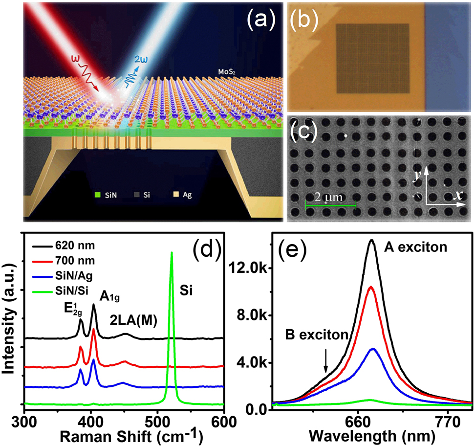
(a) Schematic of our designed sample for detecting second-harmonic generation (SHG) signal. (b) Optical microscope image of the sample with the size of 21.7 μm × 21.7 μm. (c) Scanning electron micrograph (SEM) of the structure with P = 620 nm, respectively. (d) The Raman spectra and (e) PL spectra of monolayer MoS2 on the different substrates.
At room temperature, Raman and photoluminescence (PL) spectra with a 532 nm laser excitation are detected and presented in Figure 1d and e, respectively. The monolayer MoS2 can be identified by the frequency difference between two strong Raman peaks at 384 (in-plane
In order to enhance the SHG signal of monolayer MoS2, we rational design the SPP resonance wavelength of the metallic structures covered with monolayer MoS2 to be well matched with that of fundamental wave (pump laser). Thus, plasmonic resonances properties of the designed samples with different period are firstly calculated by the frequency-domain finite-element method (FEM). We considered a metallic structure with period of 620 nm possessing a symmetric SPP resonance at wavelength 872 nm (Figure 2a), which is close to the wavelength 869.6 nm of experimental excitation laser. Here, symmetric SPP resonance mode can be identified by the electric field E z distributions with the opposite phase on the upper and lower surface which originates from the same charge accumulations (see Figure 2c) [40]. As a reference, we also chose a metallic structure with period of 700 nm, in which the excited SPPs resonances at 938 nm is far away from the wavelength of excitation laser. The experimental reflection spectra of the fabricated samples with periods of 620 and 700 nm are shown in Figure 2b. Two reflection dips induced by symmetric SPPs resonances are at wavelengths 879 and 930 nm, respectively. Slight difference maybe comes from the experimental error.

Calculated (a) and measured (b) reflection spectra with periods of 620 (black solid line) and 700 nm (red dash line), respectively. The red arrow refers to the excitation wavelength of pump laser. The electric field E z (c) and E x (d) distributions at wavelength 869.6 nm for the perforated metallic structures with period of 620 nm.
A typical laser excitation spectrum at wavelength 869.6 nm and the corresponding SHG spectra at 434.8 nm of monolayer MoS2 on the different substrates under the same incident laser power are shown in Figure 3a. An enhanced SHG effect was observed on the perforated metallic structure. The log–log scale plots of SHG output intensity in different substrates versus incident laser power are presented in Figure 3c, revealing a perfect quadratic dependence that is in agreement with the second-order nonlinear process. When the SPPs of the perforated metallic structure are in resonance with the excitation laser, monolayer MoS2 exhibits the highest SHG conversion efficiency. Comparing with the SiN/Si substrate, the SHG signal of monolayer MoS2 on the perforated metallic structure with period of 620 nm shows more than three orders of magnitude improvements.
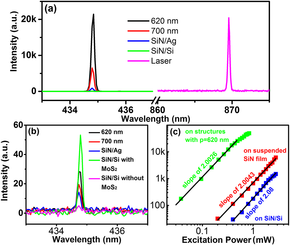
Nonlinear second-harmonic generation (SHG) microscopy. (a) SHG spectra of monolayer MoS2 on the different substrates (metallic structures with P = 620 nm (black) and P = 700 nm (red), SiN/Ag (blue) and SiN/Si (green) substrate) and typical spectrum (pink) of fundamental laser. (b) SHG spectra of the different substrates without monolayer MoS2. As a reference, SHG spectrum (green line) of the SiN/Si substrate with monolayer MoS2 is also plotted in (b). (c) The dependence of the SHG intensity from monolayer MoS2 on different substrates on the excitation power plotted in log–log scale. Quadratic linear fit is displayed by the black line.
To confirm that the experimental SHG signal comes from the monolayer MoS2, the SHG signals of the same substrate without monolayer MoS2 were measured, as plotted in Figure 3b. The SHG signal vanishes (pink line in Figure 3b) on the SiN/Si substrate due to their bulk centrosymmetric crystal structures [41]. It suggests that, the SHG signal represented by the green line in Figure 3b purely originates from monolayer MoS2. Broken inversion symmetry at metal surface and plasmon enhanced nonlinear effects [42, 43] result in appearance of SHG signal in SiN/Ag and perforated metallic substrates (Figure 3b). However, compared with monolayer MoS2 on metallic structures with P = 620 and 700 nm, the SHG signal produced by pure metallic structures is insignificant and negligible.
The SHG signal collected in the experiment is dependent on two processes: generation and detection. In generation process, the SHG intensity comes from the radiation of the second-order nonlinear polarization, which is determined by the second-order susceptibility χ
(2) and electric field E(ω) localized in the monolayer. For a monolayer MoS2 belonging to the D
3h
point-group symmetry, the second-order susceptibility tensor has a nonzero element [17]:
where E(ω) is electric field in the monolayer MoS2, which can be enhanced by the SPP resonances. C is a constant and α is an extraction coefficient determined by the fraction of SHG signal collected by the detector from the total generated SHG signal. The value of extraction coefficient depends on the nanostructure and dielectric properties of the substrate.
For comparing with the SHG signals from different substrates, the SHG enhancement factor (EF) (normalized by SHG signal on SiN/Si substrate) is defined by
where i represents different substrates. The SHG enhancement of monolayer MoS2 on perforated metallic structures mainly comes from the in-plane electric field E
x
enhancement due to the excitation of SPPs. Note that, comparing with the SiN/Si substrate the suspended MoS2 on the hole also boosts a small amount of electric field. Figure 4a and b shows the simulated in-plane electric field E
x
along z-axis with the different substrates. For the SiN/Ag and SiN/Si substrates, superposition of the incident wave and the reflected wave of the Ag and Si surfaces forms stationary wave. Out-of-phase of the reflected and incident light results in a node with weak amplitude on Ag and Si surfaces. Quantitatively, comparing with the SiN/Si substrate, the electric field EF (defined by

(a) The electric field E/E
0 distribution along z direction at the hole center of the metallic perforated structure with P = 620 (black line) and 700 nm (red line). (b) The electric field E/E
0 distribution along z direction in the SiN/Ag (black line) and SiN/Ag (red line) substrate. (c) The electric field

The measured second-harmonic generation (SHG) intensity mapping (a) and calculated total electric field distributions (b) of monolayer MoS2 on plasmonic structure with P = 620 nm, respectively. (c) The SHG intensity (black line) and electric field intensity (red line) profiles along the indicated white line in (a) and (b).
To further explore the position dependent plasmon assisted SHG enhancement, we measured the SHG mapping image for the metallic structures with a period of 620 nm, as shown in Figure 5a. One can find that, the SHG intensity is not uniformly across the sample plane (xy plane), which agree well with the calculated in-plane electric field profile at the resonant excitation wavelength (Figure 5b and c). Furthermore, one can easily get the conclusion that the increased in-plane electric fields E x localized over the holes (Figures 4 and 5) mainly contribute to SHG enhancement of monolayer MoS2. Figure 4d shows the electric field EF and SHG EF which are normalized to the hole area. Comparing with SiN/Si substrate, the normalized SHG EF of the perforated structures with period of 620 nm is 1528, which agree well with the calculated normalized electric field EF ∼ 1898. Slight difference maybe originated from reduction of extraction coefficient due to a portion of SHG signal passing through the structure via the holes. Predictably, extraction coefficient α should increase with reduced area fraction of holes due to increase of reflection. For example, for the perforated metallic structures with period of 700 nm where the area of the hole remains unchanged, due to the increased extraction coefficient and decreased electric field intensity (the symmetric SPPs resonance deviates from the excitation laser), the ultimate normalized SHG EF and electric field EF are 593 and 675 (Figure 4d), respectively.
4 Conclusions
In summary, we demonstrate the symmetric SPP enhanced SHG of monolayer MoS2 on a suspended TMDs/ultrathin-Ag-film hybrid structure with a rational designed periodic hole array. When the period of the hole array is 620 nm, the excited symmetric SPP mode is in resonance with the fundamental pump laser, leading to an SHG enhancement up to 1527 fold in the experiment at wavelength 434.5 nm. The pronounced SHG enhancement can be attributed to the distinct electric field amplification nearby the nanoholes and extraction coefficient modified by the structures. Our findings provide an effective approach to engineer the linear and nonlinear optical properties of monolayer MoS2 for various practical applications.
Funding source: National Natural Science Foundation of China
Award Identifier / Grant number: 11664020
Funding source: Anhui Provincial Natural Science Foundation
Award Identifier / Grant number: 2008085MA28
Award Identifier / Grant number: 2008085QA49
Funding source: Talent Foundation of Anhui Provincial Higher Education
Award Identifier / Grant number: gxyqZD2016189
-
Author contribution: All the authors have accepted responsibility for the entire content of this submitted manuscript and approved submission.
-
Research funding: This work was supported by the National Natural Science Foundation of China (Grant No. 12022403), and by the Anhui Provincial Natural Science Foundation (Grant Nos. 2008085MA28, 2008085QA49) and by the Fuyang Municipal Government, Fuyang Normal University Horizontal Project (Grant No. XDHX201724).
-
Conflict of interest statement: The authors declare no conflicts of interest regarding this article.
References
[1] K. F. Mark and J. Shan, “Photonics and optoelectronics of 2D semiconductor transition metal dichalcogenides,” Nat. Photonics, vol. 10, pp. 216–226, 2016.10.1038/nphoton.2015.282Search in Google Scholar
[2] L. Huang, J. Q. Liu, H. M. Deng, and S. Wu, “Phonon-like plasmonic resonances in a finitely long graphene nanoribbons array,” Adv. Opt. Mater., vol. 6, p. 1701378, 2018, https://doi.org/10.1002/adom.201701378.Search in Google Scholar
[3] J. K. Li, Z. Q. Chen, H. Yang, et al.., “Tunable broadband solar energy absorber based on monolayer transition metal dichalcogenides materials using Au nanocubes,” Nanomaterials, vol. 10, p. 257, 2020, https://doi.org/10.3390/nano10020257.Search in Google Scholar PubMed PubMed Central
[4] Q. H. Wang, K. Kalantar-Zadeh, A. Kis, et al.., “Electronics and optoelectronics of two-dimensional transition metal dichalcogenides,” Nat. Nanotechnol., vol. 7, pp. 699–712, 2012, https://doi.org/10.1038/nnano.2012.193.Search in Google Scholar PubMed
[5] K. F. Mak, C. Lee, J. Hone, et al.., “Atomically thin MoS2: A new direct-gap semiconductor,” Phys. Rev. Lett., vol. 105, p. 136805, 2010, https://doi.org/10.1103/physrevlett.105.136805.Search in Google Scholar PubMed
[6] X. Yin, Z. Ye, D. A. Chenet, et al.., “Edge nonlinear optics on a MoS2 atomic monolayer,” Science, vol. 344, pp. 488–490, 2014, https://doi.org/10.1126/science.1250564.Search in Google Scholar PubMed
[7] J. Y. You, S. R. Bongu, Q. Bao, and N. C. Panoiu, “Nonlinear optical properties and application of 2D materials: theoretical and experimental aspects,” Nanophotonics, vol. 8, pp. 63–97, 2019.10.1515/nanoph-2018-0106Search in Google Scholar
[8] A. Autere, H. Jussila, Y. Y. Dai, et al.., “Nonlinear optics with 2D layered materials,” Adv. Mater., vol. 30, p. 1705963, 2018, https://doi.org/10.1002/adma.201705963.Search in Google Scholar PubMed
[9] A. Dasgupta, J. Gao, and X. D. Yang, “Atomically thin nonlinear transition metal dichalcogenide holograms,” Nano Lett., vol. 19, pp. 6511–6516, 2019, https://doi.org/10.1021/acs.nanolett.9b02740.Search in Google Scholar PubMed
[10] K. L. Seyler, J. R. Schaibley, P. Gong, et al.., “Electrical control of second harmonic generation in a WSe2 monolayer transistor,” Nat. Nanotechnol., vol. 10, pp. 407–411, 2015, https://doi.org/10.1038/nnano.2015.73.Search in Google Scholar PubMed
[11] M. Klein, B. H. Badada, R. Binder, et al.., “2D semiconductor nonlinear plasmonic modulators,” Nat. Commun., vol. 10, p. 3264, 2019, https://doi.org/10.1038/s41467-019-11186-w.Search in Google Scholar PubMed PubMed Central
[12] D. J. Clark, V. Senthilkumar, C. T. Le, et al.., “Strong optical nonlinearity of CVD-grown MoS2 monolayer as probed by wavelength-dependent second-harmonic generation,” Phys. Rev. B, vol. 90, p. 121409(R), 2014, https://doi.org/10.1103/physrevb.90.121409.Search in Google Scholar
[13] G. Wang, X. Marie, I. Gerber, et al.., “Giant enhancement of the optical second-harmonic emission of WSe2 monolayers by laser excitation at exciton resonances,” Phys. Rev. Lett., vol. 114, p. 097403, 2015, https://doi.org/10.1103/physrevlett.114.097403.Search in Google Scholar
[14] M. Weismann and N. C. Panoiu, “Theoretical and computational analysis of second- and third-harmonic generation in periodically patterned graphene and transition-metal dichalcogenide monolayers,” Phys. Rev. B, vol. 94, p. 035435, 2016, https://doi.org/10.1103/physrevb.94.035435.Search in Google Scholar
[15] N. Kumar, S. Najmaei, Q. Cui, et al.., “Second harmonic microscopy of monolayer MoS2,” Phys. Rev. B, vol. 87, p. 161403(R), 2013, https://doi.org/10.1103/physrevb.87.161403.Search in Google Scholar
[16] J. Ribeiro-Soares, C. Janisch, Z. Liu, et al.., “Second harmonic generation in WSe2,” 2D Materials, vol. 2, p. 045015, 2015, https://doi.org/10.1088/2053-1583/2/4/045015.Search in Google Scholar
[17] L. M. Malard, T. V. Alencar, A. P. M. Barboza, et al.., “Observation of intense second harmonic generation from MoS2 atomic crystals,” Phys. Rev. B, vol. 87, p. 201401(R), 2013, https://doi.org/10.1103/physrevb.87.201401.Search in Google Scholar
[18] Y. Li, Y. Rao, K. F. Mak, et al.., “Probing symmetry properties of few-layer MoS2 and h-BN by optical second-harmonic generation,” Nano Lett., vol. 13, pp. 3329–3333, 2013, https://doi.org/10.1021/nl401561r.Search in Google Scholar PubMed
[19] L. Karvonen, A. Säynätjoki, M. J. Huttunen, et al.., “Rapid visualization of grain boundaries in monolayer MoS2 by multiphoton microscopy,” Nat. Commun., vol. 8, p. 15714, 2017, https://doi.org/10.1038/ncomms15714.Search in Google Scholar PubMed PubMed Central
[20] X. B. Yin, Z. L. Ye, D. A. Chenet, et al.., “Edge nonlinear optics on a MoS2 atomic monolayer,” Science, vol. 344, pp. 488–490, 2014, https://doi.org/10.1126/science.1250564.Search in Google Scholar PubMed
[21] X. Fan, Y. Jiang, X. Zhuang, et al.., “Broken symmetry induced strong nonlinear optical effects in spiral WS2 nanosheets,” ACS Nano, vol. 11, pp. 4892–4898, 2017, https://doi.org/10.1021/acsnano.7b01457.Search in Google Scholar PubMed
[22] X. Q. Lin, Y. Y. Liu, K. Wang, et al.., “Two-dimensional pyramid-like WS2 layered structures for highly efficient edge second-harmonic generation,” ACS Nano, vol. 12, pp. 689–696, 2018, https://doi.org/10.1021/acsnano.7b07823.Search in Google Scholar PubMed
[23] H. Chen, V. Corboliou, A. S. Solntsev, et al.., “Enhanced second-harmonic generation from two-dimensional MoSe2 on a silicon waveguide,” Light Sci. Appl., vol. 6, p. e17060, 2017, https://doi.org/10.1038/lsa.2017.60.Search in Google Scholar PubMed PubMed Central
[24] J. K. Day, M.-H. Chung, Y.-H. Lee, and V. M. Menon, “Microcavity enhanced second harmonic generation in 2D MoS2,” Opt. Mater. Express, vol. 6, pp. 2360–2365, 2016, https://doi.org/10.1364/ome.6.002360.Search in Google Scholar
[25] L. Mennel, M. Paur, and T. Mueller, “Second harmonic generation in strained transition metal dichalcogenide monolayers: MoS2, MoSe2, WS2, and WSe2,” APL Photonics, vol. 4, p. 034404, 2019, https://doi.org/10.1063/1.5051965.Search in Google Scholar
[26] P. F. Guo, S. Wu, Q. J. Ren, et al.., “Fluorescence enhancement by surface plasmon polaritons on metallic nanohole arrays,” J. Phys. Chem. Lett., vol. 1, pp. 315–318, 2010, https://doi.org/10.1021/jz900119p.Search in Google Scholar
[27] S. Wu, P. F. Guo, W. X. Huang, et al.., “Dielectric thickness detection sensor based on metallic nanohole arrays,” J. Phys. Chem. C, vol. 115, pp. 15205–15209, 2011, https://doi.org/10.1021/jp2030472.Search in Google Scholar
[28] J. Zeng, M. Yuan, W. Yuan, et al.., “Enhanced second harmonic generation of MoS2 layers on a thin gold film,” Nanoscale, vol. 7, pp. 13547–13553, 2015, https://doi.org/10.1039/c5nr03133h.Search in Google Scholar PubMed
[29] X. Q. Lin, Y. Y. Liu, K. Wang, et al.., “Hybrid three-dimensional spiral WSe2 plasmonic structures for highly efficient second-order nonlinear parametric processes,” Research, vol. 1, p. 4164029, 2018.10.1155/2018/4164029Search in Google Scholar PubMed PubMed Central
[30] J. J. Shi, Y. Li, M. Kang, et al.., “Efficient second harmonic generation in a hybrid plasmonic waveguide by mode interactions,” Nano Lett., vol. 19, pp. 3838–3845, 2019, https://doi.org/10.1021/acs.nanolett.9b01004.Search in Google Scholar PubMed
[31] Y. X. Zhang, W. Chen, T. Fu, et al.., “Simultaneous surface-enhanced resonant Raman and fluorescence spectroscopy of monolayer MoSe2: determination of ultrafast decay rates in nanometer dimension,” Nano Lett., vol. 19, pp. 6284–6291, 2019, https://doi.org/10.1021/acs.nanolett.9b02425.Search in Google Scholar PubMed
[32] J. Z. Hu, H. K. Yu, G. X. Su, et al.., “Dual-electromagnetic field enhancements through suspended metal/dielectric/metal nanostructures and plastic phthalates detection in child urine,” Adv. Opt. Mater., vol. 8, p. 1901305, 2020, https://doi.org/10.1002/adom.201901305.Search in Google Scholar
[33] F. X. Liu, B. X. Song, G. X. Su, et al.., “Sculpting extreme electromagnetic field enhancement in free space for molecule sensing,” Small, vol. 14, p. 1801146, 2018, https://doi.org/10.1002/smll.201801146.Search in Google Scholar PubMed
[34] J. Shi, W.-Y. Liang, S. S. Raja, et al.., “Plasmonic enhancement and manipulation of optical nonlinearity in monolayer tungsten disulfide,” Laser Photonics Rev., vol. 12, p. 1800188, 2018, https://doi.org/10.1002/lpor.201800188.Search in Google Scholar
[35] Z. Wang, Z. Dong, H. Zhu, et al.., “Selectively plasmon-enhanced second-harmonic generation from monolayer tungsten diselenide on flexible substrates,” ACS Nano, vol. 12, pp. 1859–1867, 2018, https://doi.org/10.1021/acsnano.7b08682.Search in Google Scholar PubMed
[36] Y. Li, A. Chernikov, X. Zhang, et al.., “Measurement of the optical dielectric function of monolayer transition-metal dichalcogenides: MoS2, MoSe2, WS2, and WSe2,” Phys. Rev. B, vol. 90, p. 205422, 2014, https://doi.org/10.1103/physrevb.90.205422.Search in Google Scholar
[37] H. H. Su, S. Wu, Y. H. Yang, et al.., “Surface plasmon polaritons enhanced photoluminescence of monolayer MoS2 on suspended periodic metallic structures,” Nanophotonics, vol. 10, pp. 975–982, 2020, https://doi.org/10.1515/nanoph-2020-0545.Search in Google Scholar
[38] L. Liang and V. Meunier, “First-principles Raman spectra of MoS2, WS2 and their heterostructures,” Nanoscale, vol. 6, pp. 5394–5401, 2014, https://doi.org/10.1039/c3nr06906k.Search in Google Scholar PubMed
[39] Y. Zhu, J. Yang, S. Zhang, et al.., “Strongly enhanced photoluminescence in nanostructured monolayer MoS2 by chemical vapor deposition,” Nanotechnology, vol. 27, p. 135706, 2016, https://doi.org/10.1088/0957-4484/27/13/135706.Search in Google Scholar PubMed
[40] S. Wu, L. Zhou, Y. M. Wang, et al.., “Phase like resonance behavior in optical transmission of sandwich coaxial square ring arrays,” Appl. Phys. Lett., vol. 96, p. 253102, 2010, https://doi.org/10.1063/1.3442498.Search in Google Scholar
[41] J. S. Levy, M. A. Foster, A. L. Gaeta, and M. Lipson, “Harmonic generation in silicon nitride ring resonators,” Opt. Express, vol. 19, pp. 11415–11421, 2011, https://doi.org/10.1364/oe.19.011415.Search in Google Scholar
[42] J. E. Sipe, D. J. Moss, and H. M. van Driel, “Phenomenological theory of optical second- and third-harmonic generation from cubic centrosymmetric crystals,” Phys. Rev. B, vol. 35, p. 1129, 1987, https://doi.org/10.1103/physrevb.35.1129.Search in Google Scholar PubMed
[43] M. Celebrano, X. Wu, M. Baselli, et al.., “Mode matching in multiresonant plasmonic nanoantennas for enhanced second harmonic generation,” Nat. Nanotechnol., vol. 10, pp. 412–417, 2015, https://doi.org/10.1038/nnano.2015.69.Search in Google Scholar PubMed
[44] Y. R. Shen, “Optical second harmonic generation at interfaces,” Annu. Rev. Phys. Chem., vol. 40, pp. 327–350, 1989, https://doi.org/10.1146/annurev.pc.40.100189.001551.Search in Google Scholar
© 2021 Qing Leng et al., published by De Gruyter, Berlin/Boston
This work is licensed under the Creative Commons Attribution 4.0 International License.
Articles in the same Issue
- Frontmatter
- Reviews
- An approach to emerging optical and optoelectronic applications based on NiO micro- and nanostructures
- Progress toward blue-emitting (460–475 nm) nanomaterials in display applications
- Research articles
- Harmonic generation with multi-layer dielectric metasurfaces
- High-efficiency and water-quenching-resistant Tb3+-based nanoparticles for single-particle imaging
- Topological guided-mode resonances at non-Hermitian nanophotonic interfaces
- Suspended silicon waveguide platform with subwavelength grating metamaterial cladding for long-wave infrared sensing applications
- Enhanced second-harmonic generation in monolayer MoS2 on suspended metallic nanostructures by plasmonic resonances
- Driving plasmonic nanoantennas at perfect impedance matching using generalized coherent perfect absorption
- Nanosecond-order long–short fluorescence lifetime switchable encryption with enlarged coding capacity
- Cooperative optical wavefront engineering with atomic arrays
- Plasmonic hot-electron photodetection with quasi-bound states in the continuum and guided resonances
- Difference-frequency generation in optically poled silicon nitride waveguides
- Three-dimensional plasmonic nano-router via optical antennas