Superlattice nonlinearities for Gigahertz-Terahertz generation in harmonic multipliers
-
Apostolos Apostolakis

 und
Mauro F. Pereira
und
Mauro F. Pereira

Abstract
Semiconductor superlattices are strongly nonlinear media offering several technological challenges associated with the generation of high-frequency Gigahertz radiation and very effective frequency multiplication up to several Terahertzs. However, charge accumulation, traps and interface defects lead to pronounced asymmetries in the nonlinear current flow, from which high harmonic generation stems. This problem requires a full non-perturbative solution of asymmetric current flow under irradiation, which we deliver in this paper within the Boltzmann-Bloch approach. We investigate the nonlinear output on both frequency and time domains and demonstrate a significant enhancement of even harmonics by tuning the interface quality. Moreover, we find that increasing arbitrarily the input power is not a solution for high nonlinear output, in contrast with materials described by conventional susceptibilities. There is a complex combination of asymmetry and power values leading to maximum high harmonic generation.
1 Introduction
The inherent nonlinearities of electronic systems can be exploited for the development of novel compact sources in the terahertz (THz) region [1], [2], [3], [4], [5]. The very same nonlinearities and their underlying microscopic origin serve as sensitive means for controlling high harmonic generation (HHG) processes. A notable very recent example is the generation of THz harmonics in a single-layer graphene due to hot Dirac fermionic dynamics under low-electric field conditions [6]. In a parallel effort, advances in strong-field and attosecond physics have paved the way to HHG in bulk crystals operating in a highly nonperturbative regime [7], [8], [9], [10], [11]. The first experimental observation of non-perturbative HHG in a bulk crystal was explained on the basis of a simple two-step model in which the nonlinearity stemmed from the anharmonicity of electronic motion in the band combined with multiple Bragg reflections at the zone boundaries [12]. The high frequency (HF) nonlinearities which contribute to harmonic upconversion in bulk semiconductors have been associated to dynamical Bloch oscillations (BO) combined with coherent interband polarization processes [7], [13]. The aforementioned models allow the use of tight-binding dispersions [14] to describe the electronic band and therefore the radiation from a nonlinear intraband current. One of the systems that demonstrate a similar highly nonparabolic energy dispersion are man-made semiconductor superlattices (SSLs) [15], [16]. In fact, the possibility of spontaneous frequency multiplication due to the effect of nonparabolicity in a SSL miniband structure was first predicted in the early works of Esaki-Tsu [17] and Romanov [18]. Superlattices are created by alternating layers of two semiconductor materials with similar lattice constants resulting in the formation of a spatial periodic potential. Furthermore, SSLs host rich dynamics in the presence of a driving field, which include the formation of Stark ladders [19], the manifestation of Bragg reflections and Bloch oscillations [20]. From the viewpoint of applications, SSLs have attracted great interest because they allow the development of devices which operate at microwave [21] and far-infrared frequencies [5], [21] suitable for high precision spectroscopic studies and detection of submillimeter waves. In addition, a considerable number of studies have tackled the task of engineering parametric amplifiers [22], [23] and frequency multipliers [24], [25], [26] based on superlattice periodic structures. Note that although the first semiconductor superlattice frequency multipliers (SSLM) were developed for the generation of microwave radiation [27], significant progress has been achieved combining high-frequency operation (up to 8.1 THz, ∼ 50th harmonic) [5], [25] and high conversion efficiency [28] comparable to the performance of Schottky diodes [28], [29].
There are various mechanisms that contribute to the HF nonlinearities of SSL devices. Once this distinction has been clearly made, it is simple to connect the underlying physical mechanisms to the frequency multiplication effects. It was found that spontaneous multiplication takes place in a dc biased tight-binding SSL, when the Bloch-oscillating electron wave packet is driven by the input oscillating field [30], [31]. Moreover, the increase of optical response [30] was due to the frequency modulation of Bloch oscillations [32], [33] which arise in the negative differential conductivity (NDC) region of the current-voltage characteristic, i. e., the current decreases with increasing bias. On the other hand, if a SSL device is in a NDC state, the nonlinearities can be further enhanced by the onset of high-field domains [34], [35] and the related propagation phenomena [36] in a similar way as the electric-field domains in bulk semiconductors [37]. Thus, the ultrafast creation and annihilation of electric domains during the time-period of an oscillating field contributes to harmonic generation processes in SSLs [38]. This type of dynamics has been found to depend on plasma effects [39], [40] induced by the space-charge instabilities and the dielectric relaxation time processes which dictate the exact conditions for the NDC state [40]. The expected THz response from BO in a miniband SSL, under the influence of a THz electric field, might also deviate due to strong excitonic effects [41], [42], [43]. Harvesting the nonlinearities discussed above can potentially lead to more efficient SSLMs or other devices suitable for achieving extremely flexible frequency tuning.
Our approach is inspired by very recent theoretical and experimental investigations [26], [44], [45], [46] of SSLM behavior, which revealed the development of even harmonics due to imperfections in the superlattice structure. In general, when an adequately strong oscillating field couples energy into the SSLM in the absence of constant bias, only odd harmonics are emitted. However, Ref. [26] showed that symmetry breaking was induced by asymmetric current flow and scattering processes under forward and reverse bias. This approach combined nonequilibrium Green’s function calculations with an Ansatz solution of the Boltzmann equation in the relaxation rate approximation. Furthermore, the asymmetric scattering rates were attributed to the different elastic (interface roughness) scattering rates which have raised from the non-identical qualities of the SSL interfaces. In general, elastic scattering processes can have a significant effect on the electron transport in SSLs.The conventional method to study the role of elastic scattering on miniband transport and generation of high-frequency radiation [47], [48] are the one dimensional (1D) SSL Balance equations [47] which can be extended to address two-dimensional and three-dimensional [49], [50] SSL transport and optical properties. They cannot, however, include systematically the different scattering processes under forward and reverse bias. A handful of experiments have been devoted to examine the harmonics of current oscillations [35], transient THz response [51], dephasing mechanisms of Bloch oscillations [52] and the electron mobility [53] under the influence of isotropic-elastic-scattering time.
In this paper, we elucidate how the effects of asymmetric scattering processes could be used to control the implications of the SL potential on the response of miniband electrons to an oscillating electric field
Our solution delivers a time-domain analysis of the mechanism responsible for the built up of high harmonic generation.
We theoretically demonstrate that the multiplication effects can be effectively controlled by special designs of superlattice interfaces (asymmetric elastic scattering).
The anisotropic effects [26] reflect that typically the interfaces of a host material (A) grown on a different host material (B) are found to be rougher than those of B on A (see Figure 1), indicating grading or intermixing of the constituent materials between SSL layers [58], [59].
![Figure 1: Schematic diagram of the origin of asymmetric current flow in a semiconductor superlattice due to differences in interface roughness depending on the sequence of layers. GaAs layers are depicted in blue (color online) and AlAs layers in gray (color online). The interface of GaAs over AlAs has lower quality than that of AlAs over GaAs. The different relaxation rates Γ+ (Γ−) depend on the direction of the time-dependent miniband velocity v(kz(ti), kz(t0)). Here t0′ and t′0${{t}^{\prime }}_{0}$ designate just different starting times [see Eq. (3)]. The SSL sample is biased by an electric field, E = (0, 0, Eac cos(2πvt)) parallel to the direction of the z–axis.](/document/doi/10.1515/nanoph-2020-0155/asset/graphic/j_nanoph-2020-0155_fig_001.jpg)
Schematic diagram of the origin of asymmetric current flow in a semiconductor superlattice due to differences in interface roughness depending on the sequence of layers. GaAs layers are depicted in blue (color online) and AlAs layers in gray (color online). The interface of GaAs over AlAs has lower quality than that of AlAs over GaAs. The different relaxation rates Γ+ (Γ−) depend on the direction of the time-dependent miniband velocity v(kz(ti), kz(t0)). Here t0′ and
This paper is organized as follows. Section 2 provides an overview of a semiclassical theory describing the charge transport in SSLs in the presence of asymmetric scattering. In Section 3, we discuss the nonlinear optical response of miniband electrons in an asymmetric SL structure and we present results of exact numerical simulations describing the spontaneous HHG. Complementary insight is provided next with time-domain calculations. In Appendix A, we revisit in more detail the path-integral expressions implemented in this work. On the other hand, Appendix B entails analytical solutions for HHG based on an Ansatz that can lead to numerical instabilities to highlight our far more efficient solution.
2 Semiclassical formulation
Throughout this work we use the standard energy dispersion,
where F is the force (−e)E corresponding to a time dependent electric field in the z–direction of the SSL and k is the total momentum which can decomposed into kz and the quasimomentum in the x–y plane k∥=(kx, ky). The right-hand side term of Eq. (1) represents the collision integral. Instead of using a single relaxation rate approximation model equivalent to
where
where kz is integrated over the Brillouin zone, the integration limits of the in-plane components k∥ are
Here v(t, t0) represents the time-dependent miniband velocity which reveals the propagation direction of the electron along the sample and therefore indicates the interaction with the high-quality or low-quality interface (see Figure 1). For a further discussion of Eqs. (2)–(4) see Appendix A. The time dependence of the velocity v(t, t0) is obtained from the set of the equations
where the parameter
The Fourier transform of the time-dependent current [Eq. (3)] can be used to obtain spectral peaks at multiples of the driving frequency. In particular, the intensity of the emitted radiation from the SSL structure is determined by the Poynting vector, which is proportional to the harmonic current term [26]
where the integration ⟨…⟩ signifies time-averaging over time interval of infinite time in the general case. Nevertheless, considering that the current response is induced merely by a monochromatic field
where ϵ0 = ϵα − 2 | T | J0(α) and
The conditions [Eq. (4)] dictate the different relaxation times
![Figure 2: (Color online) Comparison of the nonlinear response |ℐl(ν)|2${\vert {\mathrm{ℐ}}_{l}\left(\nu \right)\vert }^{2}$ characterizing the generation of second [panels (a) and (b)] and third [panels (c) and (d)] harmonics. The curves are calculated using either the path integral approach of Eq. (3) [(a) and (c)], or the ansatz of Eq. (19) [(b) and (d)] as a function of the parameter α=eEacd/(hν)$\alpha =e{E}_{ac}d/\left(h\nu \right)$ and different values of the asymmetry coefficient δ=1.05, 1.2, 1.4$\delta =1.05,\hspace{0.17em}1.2,\hspace{0.17em}1.4$. The dashed curve (c) indicates the usual third harmonic at δ = 1 whereas the vertical dashed lines [(a) and (c)] designates the critical field (a=ac)$\left(a={a}_{c}\right)$ for which the SSL can operate in the NDC part of the VI characteristic. The inset zooms on numerical instabilities for |ℐ3(ν)|2${\vert {\mathrm{ℐ}}_{3}\left(\nu \right)\vert }^{2}$ with small parameter α in the third harmonic. In all cases the frequency of the oscillating field is ν=$\nu =$ 141 GHz.](/document/doi/10.1515/nanoph-2020-0155/asset/graphic/j_nanoph-2020-0155_fig_002.jpg)
(Color online) Comparison of the nonlinear response
Before moving forward with results, we should make a brief recap of a previous research. A NEGF approach, in which the different interfaces were described by using an interface roughness self-energy, gave good agreement with static current voltage, but could not be implemented for a GHz input. Thus, this predictive input was used in a hybrid NEGF-Boltzmann equation approach by employing an analyical Ansatz solution for the asymmetric current flow [26], [44], [45], [46]. However, the Ansatz leads in some cases to numerical instabilities and errors as shown in Figure 2. This is one of the main motivations of this paper, which delivers a clean numerical solution that does not need the Ansatz. For correctness the analytical Ansatz solution is described in Appendix B.
3 Results
In this section we will investigate the effects of asymmetric scattering on HHG by implementing the approach developed in the previous section and compare its predictions to those of the analytical Ansatz solution. The basic idea is to vary the asymmetry coefficient δ which in both approaches is defined as the ratio of the different relaxation rates (
Further insight on how asymmetric effects can result in a significant gain at some even harmonic frequencies and suppression at some other odd-order harmonics, is given by the color maps in Figure 3. It shows the calculated values
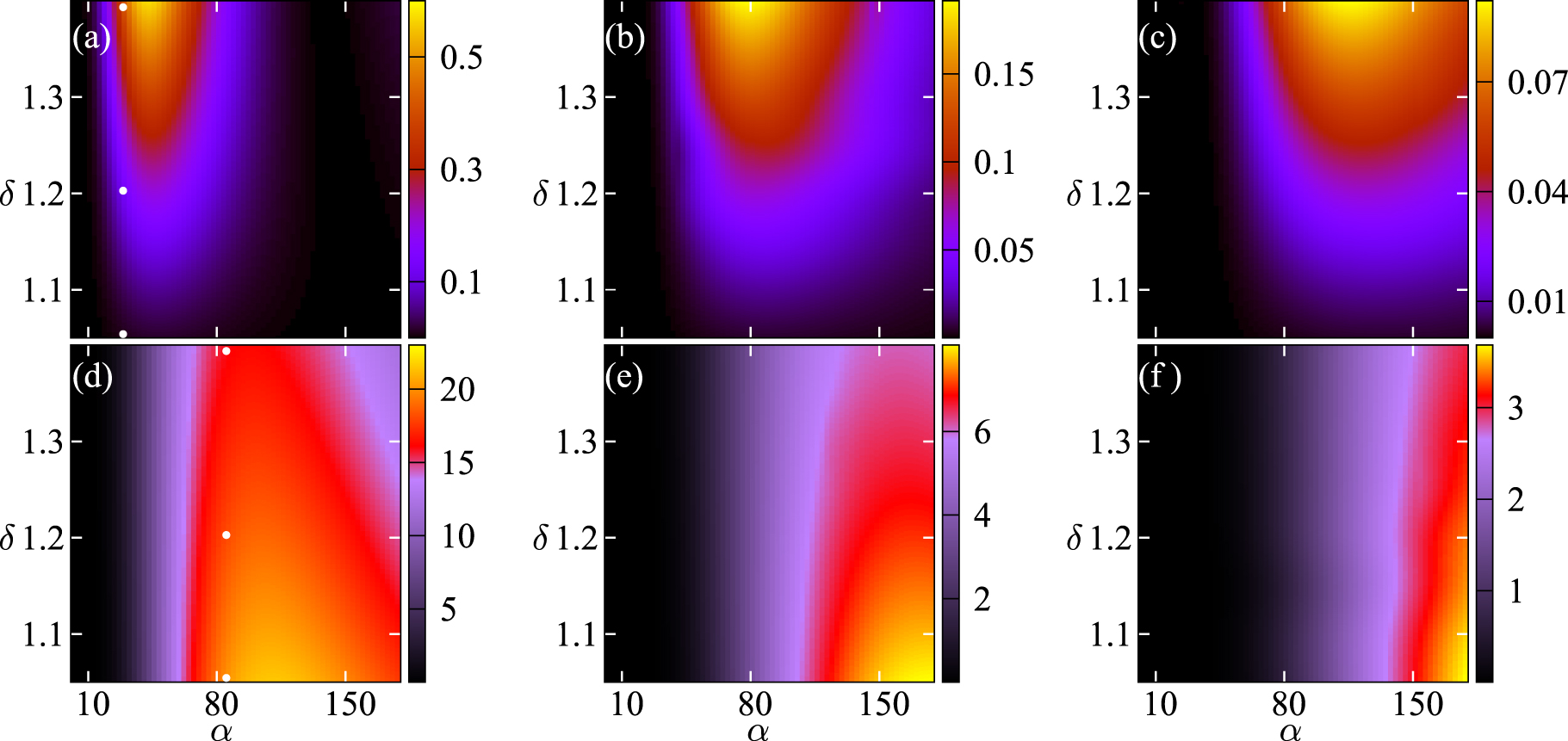
Color maps showing the dependence of the harmonic emission |ℐ(v) |2 on the parameter α and asymmetry coefficient δ for (a) l = 2, (b) l = 4, (c) l = 6, (d) l = 3, (e) l = 5 and (f) l = 7 harmonics. The white dots in panels (a) and (d) correspond to the values of α and δ used in the time domain calculations depicted in Figure 6(c) and Figure 6(d) respectively. The color bar is normalized to the peak current j0. The color maps were calculated using Eqs. (3)–(6).
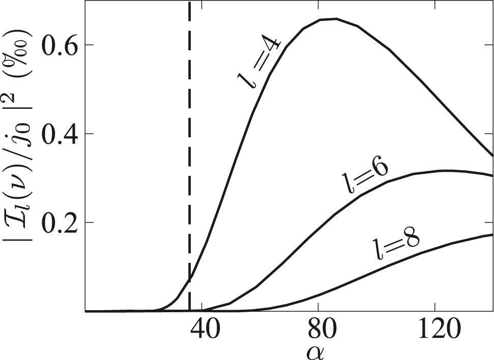
High-order even harmonics as a function of the parameter α. The asymmetry parameter is
Next, we complement the steady-state analysis with calculations of the time-dependent nonlinear response of the miniband electrons. Our time-dependent solution [see Eq. (3)] can provide further insight in the frequency-conversion of the input signal related to the asymmetric scattering processes. Figure 5 depicts the oscillating field, the nonlinear current oscillations, the second harmonic component and the third harmonic component which occur in the presence of asymmetric scattering rates. The oscillating field E(t) (see Figure 5(a)) causes a time-dependent electron drift with a time dependent current j(t) which contains different harmonic components due to the enhanced nonlinear response as shown in Figure 5(b).
![Figure 5: (Color online) Nolinear response of miniband electrons by considering asymmetric scattering processes. (a) The normalized electric field [E(t)/Eac] which causes the time dependent drift. (b) The time-dependent current j(t) [see Eq. (3)] is depicted over two cycles of the input field E(t). (c) The second-harmonic j2(t) and (d) the third-harmonic current oscillations j3(t)${j}_{3}\left(t\right)$ calculated for different values of the asymmetry parameter δ=1,1.05,1.2,1.4$\delta =1,1.05,1.2,1.4$. The labels (1) and (2) denote relevant relative minimum and maximum points. In all cases, the value of the parameter α ≃ 27 corresponds to an electric field with amplitude Ec = 0.75 Ec${E}_{c}$ and oscillating frequency ν=141$\nu =141$ GHz. The arrow marks increasing asymmetry.](/document/doi/10.1515/nanoph-2020-0155/asset/graphic/j_nanoph-2020-0155_fig_005.jpg)
(Color online) Nolinear response of miniband electrons by considering asymmetric scattering processes. (a) The normalized electric field [E(t)/Eac] which causes the time dependent drift. (b) The time-dependent current j(t) [see Eq. (3)] is depicted over two cycles of the input field E(t). (c) The second-harmonic j2(t) and (d) the third-harmonic current oscillations
![Figure 6: (Color online) Nolinear response of miniband electrons by considering asymmetric scattering processes. (a) The normalized electric field [E(t)/Eac] which causes the time dependent drift. (b) The time-dependent current j(t) [see Eq. (3)] is depicted over two cycles of the input field E(t). (c) The second-harmonic j2(t) and (d) the third-harmonic current oscillations j3(t)${j}_{3}\left(t\right)$ calculated for different values of the asymmetry parameter δ=1, 1.05, 1.2, 1.4$\delta =1,\hspace{0.17em}1.05,\hspace{0.17em}1.2,\hspace{0.17em}1.4$. The labels (1) and (2) denote relevant local minima and maxima. In all cases, the value of the parameter α ≃ 86 corresponds to an electric field with amplitude Eac = 2.4 Ec${E}_{c}$ and oscillating frequency v = 141 GHz. The arrow marks increasing asymmetry.](/document/doi/10.1515/nanoph-2020-0155/asset/graphic/j_nanoph-2020-0155_fig_006.jpg)
(Color online) Nolinear response of miniband electrons by considering asymmetric scattering processes. (a) The normalized electric field [E(t)/Eac] which causes the time dependent drift. (b) The time-dependent current j(t) [see Eq. (3)] is depicted over two cycles of the input field E(t). (c) The second-harmonic j2(t) and (d) the third-harmonic current oscillations
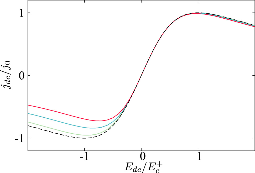
The current-voltage characteristics calculated for different values of the asymmetry parameter, from bottom (dashed) to top δ = 1,1.05,1.2, 1.4. The connection with the relaxation rates reads
In a perfectly symmetric structure, the irradiation of the superlattice with input radiation leads only to odd-order multiplication and therefore the second harmonic signal
For an electric field with sufficiently larger amplitude but with the same oscillating frequency, the current response becomes evidently more anharmonic (see Figure 6(b)). This has important implications for both second and third-order harmonics and serious consequences in the case of increasing the asymmetry parameter δ.
On the one hand, the increase of the asymmetry between the two relaxation rates results in more pronounced differences between the oscillations amplitudes (1), (2) of the second harmonic j2(t) and their adjacent peaks (Figure 6(c)). Consequently, the second harmonic is suppressed for a larger
Before summarizing the main results of this paper, it is noteworthy to highlight further immediate applications of our approach. Evidently the electron energy oscillates within the miniband with frequency at every even multiple of the frequency of the oscillating electric field [see Eq. (3)]. The behavior of effective electron mass, which explicitly depends on energy [66], varies significantly in the presence of highly asymmetric scattering and thus the generated harmonics could be linked to the concept of negative effective mass similar to [67]. Significant production of even harmonics has been previously predicted for an electrically excited SSL due to parametric amplification [68] or other parametric processes [60] which stem from the existence of an internal electric field in the structure. In this respect, it is interesting to study how the parametric processes can affect the harmonic generation [70] or the Bloch gain [69] profile in the presence of asymmetric current flow. Moreover, our approach has a great potential for analyzing the effects of asymmetric scattering processes on the intensity of harmonics by means of externally applied voltages and/or intense ultrafast optical pulses [51], [43]. Finally, the predictions in the present work highlight the prospects for the systematic study of asymmetric effects in different superlattice systems including coupled superlattices in a synchronous state [71] and, even more generally, in other multilayer structures such as high temperature superconductors [72].
4 Conclusions
In summary, the Boltzmann-Bloch approach is used to deliver general, non-perturbative solutions of HHG in SSLs. This method allows us to investigate details of the generation processes in both spectral and time domains. The non-approximative nature of our approach eliminates numerical errors which could cast doubt upon the origin of harmonic generation. Thus, our study conclusively demonstrates striking features of HHG when asymmetric relaxation processes are taken into account in superlattice structures. While these effects are relatively small on the odd harmonic generation, significant features appear at even harmonics leading to measurable effects in the GHz-THz range. Our algorithms have immediate potential to analyze the combination of asymmetric flow with parametric processes, externally applied voltages and ultrafast optical pulses.Future work should focus on investigating thoroughly the conditions for formation of destructive electric domains in SSLs in the case of harmonic generation due to asymmetric scattering processes.
Funding source: Czech Science Foundation (GACR)
Award Identifier / Grant number: 19-03765
Funding source: EU H2020-Europe’s resilience to crises and disasters program
Award Identifier / Grant number: 832876, AQUA3S
A Formulations of superlattice transport equations
In this section, we revisit expressions describing a solution to SSL transport problems and having as a starting point the Boltzmann equation. The general formalism has been applied to describe transport in semiconducting devices [73], parametric amplification [22] and Bloch gain [74] in spatially homogeneous SSLs. This method allows us to deliver a general numerical solution for the influence of asymmetric relaxation effects on miniband transport model and frequency multiplication processes in superlattices in the presence of an oscillating electric field, eliminating the need for the approximative Ansatz used in Refs. [26], [44], [45], [46]. The electron distribution function
The second term of the right-hand side of Eq. (8) represents the rate of change of f due to collisions, which is characterized conventionally by the transition probability W(k′, k)dk per unit time that an electron will be scattered out of a state k into a volume element dk and the rate W(k, k)dk per unit tame that an electron with wave vector k will scatter to a state whose vector lies between k′ and
Thus, if a single and isotropic (same for all states k) relaxation rate is assumed then
We would like to localize the asymmetry of the electron scattering function due to interface roughness to well-defined regions of the SSL. Therefore, we assume that W(kz′, kz(t0)) = W0 if kz′ and kz and both lie in within a region of the miniband for which vz(kz′, kz(t0)) > 0, otherwise
and
indicating the existence of two scattering rates due to differences in interface roughness depending on the sequence of the layers. Here for simplicity we designate the region in k-space as
Note that the static current jdc is obtained by taking
Figure 7 demonstrates jdc versus
B Ansatz analytical solution
In this section we will give a recap of the analytical ansatz solution previously used to describe asymmetric current flow and the effects of asymmetric scattering on HHG [26], [44], [45], [46]. Thus, one can consider a SSL with period d under an electric field
where the dc current
where the potential energy U is equal to integer number of photon quanta
Acknowledgment
The authors acknowledge access to computing and storage facilities owned by parties and projects contributing to the National Grid Infrastructure MetaCentrum provided under the programme “Projects of Large Research, Development, and Innovations Infrastructures” (CESNET LM2015042) is greatly appreciated.
Author contribution: All the authors have accepted responsibility for the entire content of this submitted manuscript and approved submission.
Research funding: The authors acknowledge support by the Czech Science Foundation (GAČR) through grant No. 19-03765, the EU H2020-Europe’s resilience to crises and disasters program (No. 832876, aqua3S) and Khalifa University of Science and Technology under Award No. CPRA-2020-Breathan.
Conflict of interest statement: The authors declare no conflicts of interest regarding this article.
References
[1] S. Dhillon, M. Vitiello, E. Linfield, et al., “The 2017 terahertz science and technology roadmap,” J. Phys. Appl. Phys., vol. 50, no. 4, p. 043001, 2017, https://doi.org/10.1088/1361-6463/50/4/043001.Suche in Google Scholar
[2] M. Tonouchi, “Cutting-edge terahertz technology,” Nat. photon., vol. 1, no. 2, p. 97, 2007, https://doi.org/10.1038/nphoton.2007.3.Suche in Google Scholar
[3] F. Blanchard, G. Sharma, L. Razzari, et al., “Generation of intense terahertz radiation via optical methods,” IEEE J. Sel. Top. Quant. Electron., vol. 17, no. 1, pp. 5–16, 2010, https://doi.org/10.1109/JSTQE.2010.2047715.Suche in Google Scholar
[4] Z. Chen and R. Morandotti, Nonlinear Photonics and Novel Optical Phenomena, Berlin, Germany, Springer, 2012.10.1007/978-1-4614-3538-9Suche in Google Scholar
[5] V. Vaks, “High-precise spectrometry of the terahertz frequency range: the methods, approaches and applications,” J. Infrared, Millim. Terahertz Waves, vol. 33, no. 1, pp. 43–53, 2012, https://doi.org/10.1007/s10762-011-9846-x.Suche in Google Scholar
[6] H. A. Hafez, S. Kovalev, J. C. Deinert, et al., “Extremely efficient terahertz high-harmonic generation in graphene by hot Dirac fermions,” Nature, vol. 561, no. 7724, p. 507, 2018, https://doi.org/10.1038/s41586-018-0508-1.Suche in Google Scholar PubMed
[7] O. Schubert, M. Hohenleutner, F. Langer, et al., “Sub-cycle control of terahertz high-harmonic generation by dynamical bloch oscillations,” Nat. Photon., vol. 8, no. 2, p. 119, 2014, https://doi.org/10.1038/nphoton.2013.349.Suche in Google Scholar
[8] F. Langer, M. Hohenleutner, C. Schmid, et al., “Lightwave-driven quasiparticle collisions on a subcycle timescale,” Nature, vol. 533, p. 225, 2016, https://doi.org/10.1038/nature17958.Suche in Google Scholar PubMed PubMed Central
[9] M. Drescher, M. Hentschel, R. Kienberger, et al., “X-ray pulses approaching the attosecond Frontier,” Science, vol. 291, pp. 1923–1927, 2001, https://doi.org/10.1126/science.1058561.Suche in Google Scholar PubMed
[10] O. Smirnova, Y. Mairesse, S. Patchkovskii, et al., “High harmonic interferometry of multi-electron dynamics in molecules,” Nature, vol. 460, p. 972, 2009, https://doi.org/10.1038/nature08253.Suche in Google Scholar PubMed
[11] F. Krausz and M. Ivanov, “Attosecond physics,” Rev. Mod. Phys., vol. 81, p. 163, 2009, https://doi.org/10.1103/revmodphys.81.163.Suche in Google Scholar
[12] S. Ghimire, A. D. DiChiara, E. Sistrunk, et al., “Observation of high-order harmonic generation in a bulk crystal,” Nat. Phys., vol. 7, p. 138, 2011, https://doi.org/10.1038/nphys1847.Suche in Google Scholar
[13] M. Hohenleutner, F. Langer, O. Schubert, et al., “Realtime observation of interfering crystal electrons in high-harmonic generation,” Nature, vol. 523, p. 572, 2015, https://doi.org/10.1038/nature14652.Suche in Google Scholar
[14] D. Golde, T. Meier, and S. W. Koch, “High harmonics generated in semiconductor nanostructures by the coupled dynamics of optical inter-and intraband excitations,” Phys. Rev. B, vol. 77, p. 075330, 2008, https://doi.org/10.1103/physrevb.77.075330.Suche in Google Scholar
[15] L. Esaki and R. Tsu, “Superlattice and negative differential conductivity in semiconductors,” IBM J. Res. Dev., vol. 14, pp. 61–65, 1970, https://doi.org/10.1147/rd.141.0061.Suche in Google Scholar
[16] A. Wacker, “Semiconductor superlattices: a model system for nonlinear transport,” Phys. Rep., vol. 357, pp. 1–111, 2002, https://doi.org/10.1016/s0370-1573(01)00029-1.Suche in Google Scholar
[17] R. Tsu and L. Esaki, “Nonlinear optical response of conduction electrons in a superlattice,” Appl. Phys. Lett., vol. 19, pp. 246–248, 1971, https://doi.org/10.1063/1.1653904.Suche in Google Scholar
[18] Y. A. Romanov, “Nonlinear effects in periodic semiconductor structures (frequency multiplication due to nonparabolicity of dispersion law in semiconductor structure subbands, noting electromagnetic signal transformation),” Opt. Spectra, vol. 33, pp. 917–920, 1972.Suche in Google Scholar
[19] E. E. Mendez, F. Agullo-Rueda, and J. M. Hong, “Stark localization in gaas-gaalas superlattices under an electric field,” Phys. Rev. Lett., vol. 60, p. 2426, 1988, https://doi.org/10.1103/physrevlett.60.2426.Suche in Google Scholar PubMed
[20] C. Waschke, H. G. Roskos, R. Schwedler, et al., “Coherent submillimeter-wave emission from bloch oscillations in a semiconductor superlattice,” Phys. Rev. Lett., vol. 70, p. 3319, 1993, https://doi.org/10.1103/physrevlett.70.3319.Suche in Google Scholar
[21] P. Khosropanah, A. Baryshev, W. Zhang, et al., “Phase locking of a 2.7 THz quantum cascade laser to a microwave reference,” Opt. Lett., vol. 34, pp. 2958–2960, 2009, https://doi.org/10.1364/ol.34.002958.Suche in Google Scholar PubMed
[22] K. F. Renk, B. I. Stahl, A. Rogl, et al., “Subterahertz superlattice parametric oscillator,” Phys. Rev. Lett., vol. 95, p. 126801, 2005, https://doi.org/10.1103/physrevlett.95.126801.Suche in Google Scholar PubMed
[23] K. F. Renk, A. Rogl, and B. I. Stahl, “Semiconductorsuperlattice parametric oscillator for generation of sub-terahertz and terahertz waves,” J. Lumin., vol. 125, pp. 252–258, 2007, https://doi.org/10.1016/j.jlumin.2006.08.037.Suche in Google Scholar
[24] F. Klappenberger, K. F. Renk, P. Renk, et al., “Semiconductor–superlattice frequency multiplier for generation of submillimeter waves,” Appl. Phys. Lett., vol. 84, pp. 3924–3926, 2004, https://doi.org/10.1063/1.1741037.Suche in Google Scholar
[25] D. G. Paveliev, Y. I. Koshurinov, A. S. Ivanov, et al., “Experimental study of frequency multipliers based on a GaAs/AlAs semiconductor superlattices in the terahertz frequency range,” Semiconductors, vol. 46, pp. 121–125, 2012, https://doi.org/10.1134/s1063782612010150.Suche in Google Scholar
[26] M. F. Pereira, J. P. Zubelli, D. Winge, et al., “Theory and measurements of harmonic generation in semiconductor superlattices with applications in the 100 GHz to 1 THz range,” Phys. Rev. B, vol. 96, p. 045306, 2017, https://doi.org/10.1103/physrevb.96.045306.Suche in Google Scholar
[27] J. Grenzer, A. A. Ignatov, E. Schomburg, et al., “Microwave oscillator based on bloch oscillations of electrons in a semiconductor superlattice,” Ann. Phys., vol. 507, pp. 184–190, 1995, https://doi.org/10.1002/andp.19955070304.Suche in Google Scholar
[28] C. P. Endres, F. Lewen, T. F. Giesen, et al., “Application of superlattice multipliers for high-resolution terahertz spectroscopy,” Rev. Sci. Instrum., vol. 78, p. 043106, 2007, https://doi.org/10.1063/1.2722401.Suche in Google Scholar PubMed
[29] J. V. Siles and J. Grajal, “Physics-based design and optimization of Schottky diode frequency multipliers for terahertz applications,” IEEE Trans. Microw. Theor. Tech., vol. 58, pp. 1933–1942, 2010, https://doi.org/10.1109/tmtt.2010.2050103.Suche in Google Scholar
[30] S. Winnerl, E. Schomburg, S. Brandl, et al., “Frequency doubling and tripling of terahertz radiation in a GaAs/AlAs superlattice due to frequency modulation of bloch oscillations,” Appl. Phys. Lett., vol. 77, pp. 1259–1261, 2000, https://doi.org/10.1063/1.1290141.Suche in Google Scholar
[31] E. Schomburg, J. Grenzer, K. Hofbeck, et al., “Superlattice frequency multiplier for generation of submillimeter waves,” IEEE J. Sel. Top. Quant. Electron., vol. 2, pp. 724–728, 1996, https://doi.org/10.1109/2944.571773.Suche in Google Scholar
[32] A. A. Ignatov, E. Schomburg, J. Grenzer, et al., “THz-field induced nonlinear transport and dc voltage generation in a semiconductor superlattice due to bloch oscillations,” Z. Phys. B, vol. 98, pp. 187–195, 1995, https://doi.org/10.1007/bf01324524.Suche in Google Scholar
[33] Y. A. Romanov and Y. Y. Romanova, “Bloch oscillations in superlattices: the problem of a terahertz oscillator,” Semiconductors, vol. 39, pp. 147–155, 2005, https://doi.org/10.1134/1.1852666.Suche in Google Scholar
[34] H. Le Person, C. Minot, L. Boni, et al., “Gunn oscillations up to 20 GHz optically induced in GaAs/AlAs superlattice,” Appl. Phys. Lett., vol. 60, pp. 2397–2399, 1992, https://doi.org/10.1063/1.106984.Suche in Google Scholar
[35] E. Schomburg, T. Blomeier, K. Hofbeck, et al., “Current oscillation in superlattices with different miniband widths,” Phys. Rev. B, vol. 58, p. 4035, 1998, https://doi.org/10.1103/physrevb.58.4035.Suche in Google Scholar
[36] V. V. Makarov, A. E. Hramov, A. A. Koronovskii, et al., “Sub-terahertz amplification in a semiconductor superlattice with moving charge domains,” Appl. Phys. Lett., vol. 106, p. 043503, 2015, https://doi.org/10.1063/1.4906531.Suche in Google Scholar
[37] J. Gunn, “Instabilities of current in iii–v semiconductors,” IBM J. Res. Dev., vol. 8, pp. 141–159, 1964, https://doi.org/10.1147/rd.82.0141.Suche in Google Scholar
[38] R. Scheuerer, M. Haeussler, K. F. Renk, et al., “Frequency multiplication of microwave radiation by propagating space-charge domains in a semiconductor superlattice,” Appl. Phys. Lett., vol. 82, pp. 2826–2828, 2003, https://doi.org/10.1063/1.1569999.Suche in Google Scholar
[39] B. R. Pamplin, “Negative differential conductivity effects in semiconductors,” Contemp. Phys., vol. 11, pp. 1–19, 1970, https://doi.org/10.1080/00107517008204806.Suche in Google Scholar
[40] F. Klappenberger, K. N. Alekseev, K. F. Renk, et al., “Ultrafastcreation and annihilation of space-charge domains in a semiconductor superlattice observed by use of terahertz fields,” Eur. Phys. J. B, vol. 39, pp. 483–489, 2004, https://doi.org/10.1140/epjb/e2004-00221-y.Suche in Google Scholar
[41] T. Meier, G. Von Plessen, P. Thomas, et al., “Coherent electric-field effects in semiconductors,” Phys. Rev. Lett., vol. 73, p. 902, 1994, https://doi.org/10.1103/physrevlett.73.902.Suche in Google Scholar PubMed
[42] M. Dignam, “Excitonic bloch oscillations in a terahertz field,” Phys. Rev. B, vol. 59, p. 5770, 1999, https://doi.org/10.1103/physrevb.59.5770.Suche in Google Scholar
[43] D. Wang, A. Zhang, L. Yang, et al., “Tunable terahertz amplification in optically excited biased semiconductor superlattices: influence of excited excitonic states,” Phys. Rev. B, vol. 77, p. 115307, 2008, https://doi.org/10.1103/physrevb.77.115307.Suche in Google Scholar
[44] M. F. Pereira, V. A. Anfertev, J. P. Zubelli, et al., “Terahertz generation by gigahertz multiplication in superlattices,” J. Nanophoton., vol. 11, p. 046022, 2017, https://doi.org/10.1117/1.jnp.11.046022.Suche in Google Scholar
[45] A. Apostolakis and M. F. Pereira, “Controlling the harmonic conversion efficiency in semiconductor superlattices by interface roughness design,” AIP Adv., vol. 9, p. 015022, 2019, https://doi.org/10.1063/1.5050917.Suche in Google Scholar
[46] A. Apostolakis and M. F. Pereira, “Potential and limits of superlattice multipliers coupled to different inputpower sources,” J. Nanophoton., vol. 13, pp. 1–11, 2019, https://doi.org/10.1117/1.jnp.13.036017.Suche in Google Scholar
[47] A. A. Ignatov, E. P Dodin, and V. I Shashkin, “Transient response theory of semiconductor superlattices: connection with bloch oscillations,” Mod. Phys. Lett. B, vol. 5, pp. 1087–1094, 1991, https://doi.org/10.1142/s0217984991001337.Suche in Google Scholar
[48] K. N. Alekseev, E. H Cannon, J. C McKinney, et al., “Spontaneousdc current generation in a resistively shunted semiconductor superlattice driven by a terahertz field,” Phys. Rev. Lett., vol. 80, p. 2669, 1998, https://doi.org/10.1103/physrevlett.80.2669.Suche in Google Scholar
[49] R. R. Gerhardts, “Effect of elastic scattering on miniband transport in semiconductor superlattices,” Phys. Rev. B, vol. 48, p. 9178, 1993, https://doi.org/10.1103/physrevb.48.9178.Suche in Google Scholar PubMed
[50] Y. A. Romanov, J. Y Romanova, L. G Mourokh, et al., “Self-induced and induced transparencies of twodimensional and three-dimensional superlattices,” Phys. Rev. B, vol. 66, p. 045319, 2002, https://doi.org/10.1103/physrevb.66.045319.Suche in Google Scholar
[51] R. Ferreira, T. Unuma, K. Hirakawa, et al., “A Boltzmann approach to transient Bloch emission from semiconductor superlattices,” Appl. Phys. Express, vol. 2, p. 062101, 2009, https://doi.org/10.1143/apex.2.062101.Suche in Google Scholar
[52] T. Unuma, N. Sekine, and K. Hirakawa, “Dephasing of bloch oscillating electrons in GaAs-based superlattices due to interface roughness scattering. Appl. phys. Lett., vol. 89, p. 161913, 2006, https://doi.org/10.1063/1.2360911.Suche in Google Scholar
[53] H. Sakaki, T. Noda, K. Hirakawa, et al., “Interface roughness scattering in GaAs/AlAs quantum wells,” Appl. phys. Lett., vol. 51, pp. 1934–1936, 1987, https://doi.org/10.1063/1.98305.Suche in Google Scholar
[54] R. G. Chambers, “The kinetic formulation of conduction problems,” Proc. Phys. Soc. Sec. A, vol. 65, p. 458, 1952, https://doi.org/10.1088/0370-1298/65/6/114.Suche in Google Scholar
[55] A. Ignatov and Y. A. Romanov, “Nonlinear electromagnetic properties of semiconductors with a superlattice,” Phys. Status Solidi B, vol. 73, pp. 327–333, 1976, https://doi.org/10.1002/pssb.2220730132.Suche in Google Scholar
[56] G. M. Shmelev, I. I. Maglevanny, and A. S. Bulygin, “Currentvoltage characteristic of asymmetric superlattice,” Phys. C Supercond., vol. 292, pp. 73–78, 1997, https://doi.org/10.1016/s0921-4534(97)01640-7.Suche in Google Scholar
[57] G. M. Shmelev, N. A. Soina, and I. I. Maglevanny, “Highfrequency conductivity of an asymmetric superlattice,” Phys. Solid State, vol. 40, pp. 1574–1576, 1998, https://doi.org/10.1134/1.1130600.Suche in Google Scholar
[58] R. M. Feenstra, D. A. Collins, D. Y. Ting, et al., “Interface roughness and asymmetry in InAs/GaSb superlattices studied by scanning tunneling microscopy,” Phys. Rev. Lett., vol. 72, p. 2749, 1994, https://doi.org/10.1103/physrevlett.72.2749.Suche in Google Scholar
[59] Y. Tokura, T. Saku, S. Tarucha, et al., “Anisotropic roughness scattering at a heterostructure interface,” Phys. Rev. B, vol. 46, p. 15558, 1992, https://doi.org/10.1103/physrevb.46.15558.Suche in Google Scholar PubMed
[60] N. W. Ashcroft and N. D. Mermin, Solid State Physics. Philadelphia, Saunders College, 1976.Suche in Google Scholar
[61] M. Abramowitz and I. A. Stegun, Handbook of Mathematical Functions, New York, Dover Publications, 1972.Suche in Google Scholar
[62] A. Patanè, D. Sherwood, L. Eaves, et al., “Tailoring the electronic properties of GaAs/AlAs superlattices by inas layer insertions,” Appl. Phys. Lett., vol. 81, pp. 661–663, 2002, https://doi.org/10.1063/1.1496140.Suche in Google Scholar
[63] T. M. Fromhold, A. Patane, S. Bujkiewicz, et al., “Chaotic electron diffusion through stochastic webs enhances current flow in superlattices,” Nature, vol. 428, p. 726, 2004, https://doi.org/10.1038/nature02445.Suche in Google Scholar PubMed
[64] M. T. Greenaway, A. G. Balanov, E. Schöll, et al., “Controlling and enhancing terahertz collective electron dynamics in superlattices by chaos-assisted miniband transport,” Phys. Rev. B, vol. 80, p. 205318, 2009, https://doi.org/10.1103/physrevb.80.205318.Suche in Google Scholar
[65] W. H. Press, S. A. Teukolsky, W. T. Vetterling, et al., Numerical Recipes in Fortran 77: The Art of Scientific Computing. Cambridge, Cambridge University Press, 1992.Suche in Google Scholar
[66] A. A. Ignatov, K. F. Renk, E. P. Dodin, “Esaki-Tsu superlattice oscillator: josephson-like dynamics of carriers,” Phys. Rev. Lett., vol. 70, p. 1996, 1993, https://doi.org/10.1103/physrevlett.70.1996.Suche in Google Scholar PubMed
[67] A. V. Shorokhov, M. A. Pyataev, N. N. Khvastunov, et al., “Physical principles of the amplification of electromagnetic radiation due to negative electron masses in a semiconductor superlattice,” JETP Lett., vol. 100, pp. 766–770, 2015, https://doi.org/10.1134/s002136401424014x.Suche in Google Scholar
[68] T. Hyart, N. V. Alexeeva, A. Leppänen, et al., “Terahertz parametric gain in semiconductor superlattices in the absence of electric domains,” Appl. Phys. Lett., vol. 89, p. 132105, 2006, https://doi.org/10.1063/1.2357579.Suche in Google Scholar
[69] Y. A. Romanov and Y. Y. Romanova, “Self-oscillations in semiconductor superlattices,” J. Exp . Theor. Phys., vol. 91, pp. 1033–1045, 2000, https://doi.org/10.1134/1.1334994.Suche in Google Scholar
[70] T. Hyart, A. V. Shorokhov, and K. N. Alekseev, “Theory of parametric amplification in superlattices,” Phys. Rev. Lett., vol. 98, p. 220404, 2007, https://doi.org/10.1103/physrevlett.98.220404.Suche in Google Scholar
[71] S. Matharu, F. V. Kusmartsev, and A. G. Balanov, “Highfrequency generation in two coupled semiconductor superlattices,” Eur. Phys. J. Spec. Top., vol. 222, pp. 2559–2570, 2013, https://doi.org/10.1140/epjst/e2013-02037-4.Suche in Google Scholar
[72] V. A. Yampol’skii, S. Savel’ev, O. V. Usatenko, et al., “Controlled terahertz frequency response and transparency of Josephson chains and superconducting multilayers,” Phys. Rev. B, vol. 75, p. 014527, 2007, https://doi.org/10.1103/PhysRevB.75.014527.Suche in Google Scholar
[73] H. Budd, “Path variable formulation of the hot carrier problem,” Phys. Rev., vol. 158, p. 798, 1967, https://doi.org/10.1103/physrev.158.798.Suche in Google Scholar
[74] T. Hyart, J. Mattas, K. N. Alekseev, “Model of the influence of an external magnetic field on the gain of terahertz radiation from semiconductor superlattices,” Phys. Rev. Lett., vol. 103, p. 117401, 2009, https://doi.org/10.1103/physrevlett.103.117401.Suche in Google Scholar
[75] A. Wacker, A. P. Jauho, S. Zeuner, et al., “Sequential tunneling in doped superlattices: fingerprints of impurity bands and photon-assisted tunneling,” Phys. Rev. B, vol. 56, pp. 13268–13278, 1997, https://doi.org/10.1103/physrevb.56.13268.Suche in Google Scholar
© 2020 Apostolos Apostolakis et al., published by De Gruyter, Berlin/Boston
This work is licensed under the Creative Commons Attribution 4.0 International License.
Artikel in diesem Heft
- Editorial
- Interdisciplinary nanophotonics
- Reviews
- Advances in exploiting the degrees of freedom in nanostructured metasurface design: from 1 to 3 to more
- On-chip nanophotonics and future challenges
- All-dielectric metasurfaces for polarization manipulation: principles and emerging applications
- Nonlinear nanophotonic devices in the ultraviolet to visible wavelength range
- Active plasmonic nanoantenna: an emerging toolbox from photonics to neuroscience
- Research Articles
- Simply synthesized nitrogen-doped graphene quantum dot (NGQD)-modified electrode for the ultrasensitive photoelectrochemical detection of dopamine
- Design and optimization of tunneling photodetectors based on graphene/Al2O3/silicon heterostructures
- Self-induced thermo-optical effects in silicon and germanium dielectric nanoresonators
- Plasmon-controlled, ultra-bright, excitation-polarization-independent photoluminescence from individual Ag nanoplates
- Passively Q-switched Yb-doped all-fiber laser based on Ag nanoplates as saturable absorber
- Stacking angle dependent multiple excitonic resonances in bilayer tungsten diselenide
- Optically and radio frequency (RF) transparent meta-glass
- Critical review of quantum plasmonic models for finite-size media
- Tunable plasmon-phonon polaritons in anisotropic 2D materials on hexagonal boron nitride
- Pixeled metasurface for multiwavelength detection of vitamin D
- Phase-controlled metasurface design via optimized genetic algorithm
- Superlattice nonlinearities for Gigahertz-Terahertz generation in harmonic multipliers
- Multipolar second-harmonic generation from high-Q quasi-BIC states in subwavelength resonators
- Lasing at the nanoscale: coherent emission of surface plasmons by an electrically driven nanolaser
- Perovskite nanowire lasers on low-refractive-index conductive substrate for high-Q and low-threshold operation
- A simple transfer-matrix model for metasurface multilayer systems
- Enhanced two-photon photoluminescence assisted by multi-resonant characteristics of a gold nanocylinder
- Nanoscale control of single molecule Förster resonance energy transfer by a scanning photonic nanoantenna
- Magnetic switching of Kerker scattering in spherical microresonators
- High-efficiency, large-area lattice light-sheet generation by dielectric metasurfaces