Robust optical physical unclonable function using disordered photonic integrated circuits
-
Farhan Bin Tarik


Abstract
Physical unclonable function (PUF) has emerged as a promising and important security primitive for use in modern systems and devices, due to their increasingly embedded, distributed, unsupervised, and physically exposed nature. However, optical PUFs based on speckle patterns, chaos, or ‘strong’ disorder are so far notoriously sensitive to probing and/or environmental variations. Here we report an optical PUF designed for robustness against fluctuations in optical angular/spatial alignment, polarization, and temperature. This is achieved using an integrated quasicrystal interferometer (QCI) which sensitively probes disorder while: (1) ensuring all modes are engineered to exhibit approximately the same confinement factor in the predominant thermo-optic medium (e. g. silicon), and (2) constraining the transverse spatial-mode and polarization degrees of freedom. This demonstration unveils a new means for amplifying and harnessing the effects of ‘weak’ disorder in photonics and is an important and enabling step toward new generations of optics-enabled hardware and information security devices.
1 Main Text
Disorder and entropy are pervasive characteristics of nature and can be harnessed by physical unclonable functions (PUFs) [1], [2], [3], [4], [5] or random number generators [6], [7], to achieve significantly higher levels of hardware and/or information security than conventional methods. Manufacturing process variations are among the most technologically relevant forms of such randomness and are the primary means by which PUFs extract their chip-unique signatures [1], [2], [3], [8], [9], [10]. Recently, classical time-varying PUFs have been applied in secure communications [11] and in schemes obtaining perfect secrecy cryptography [12]. In another highly demanded application, PUFs have emerged as promising security primitives for authentication and identification throughout the untrusted supply chain as illustrated in Figure 1.
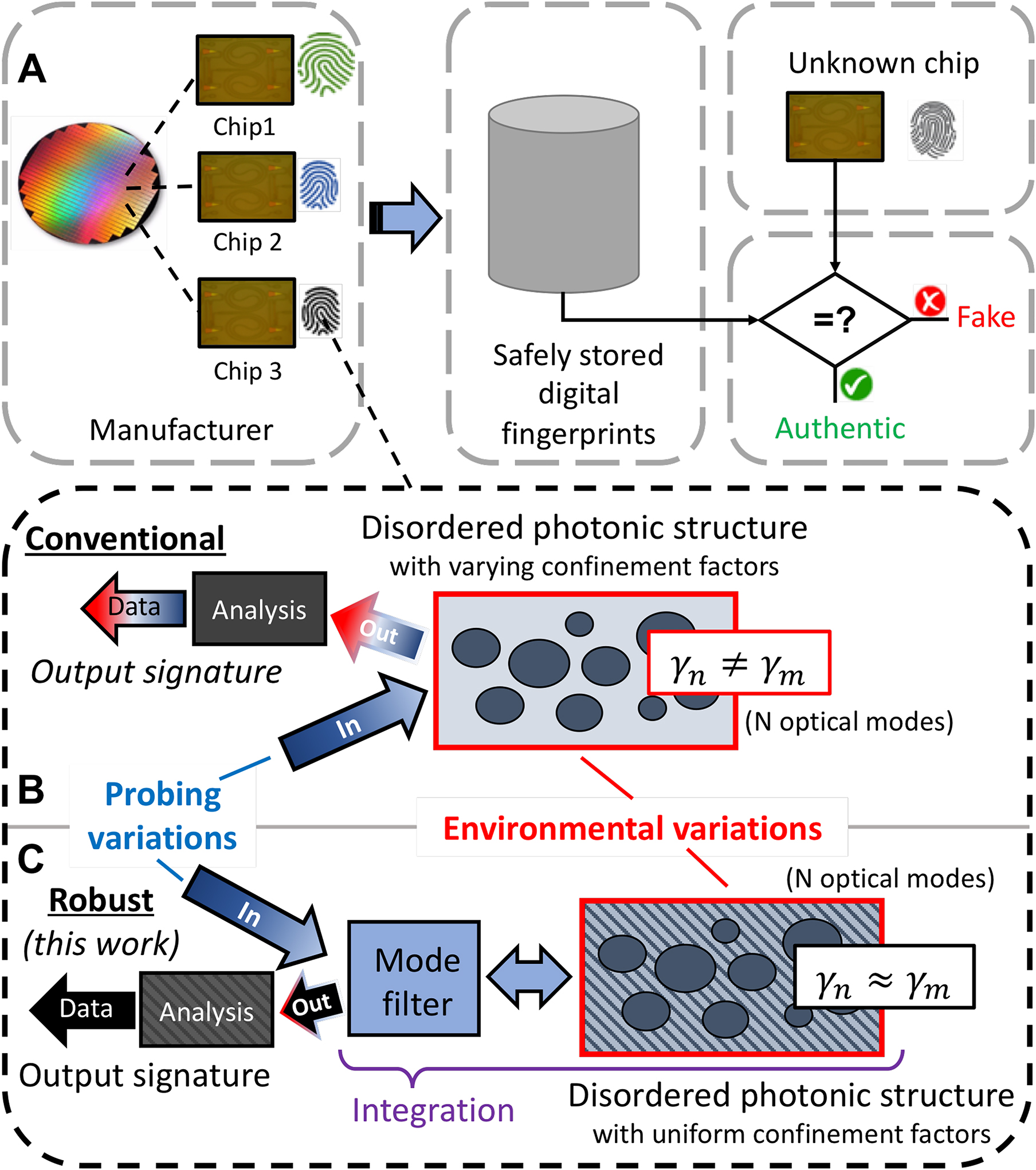
High level overview. (A) A typical PUF authentication scheme, and overview of: (B) a conventional optical PUF, and (C) a robust optical PUF (the type introduced and demonstrated in this work). Here robustness refers to achieving immunity against probing and environmental variations.
Much of the technological progress in PUFs over the last 15 plus years has come in complementary metal oxide semiconductor (CMOS) micro- and nanoelectronics [13], [14], [15], [16], [17]. However, interest in developing PUFs for hardware and information security applications has recently rapidly expanded to almost all areas of physical science including investigations based on chemical methods [18], quantum tunneling [19], disordered nanomaterials [20], [21], [22], magnetic media [23], and even biological species [24]. Attractively, the immense information capacity and rich physics of photonic systems offer the prospect of both passive and active security devices operating in classical and quantum regimes [1], [25], [26]. Moreover, highly complex and distributed multiple-scattering optical systems with high fabrication sensitivities can be very difficult to model or trim. Thus, the question remains open as to whether emerging technology could enable successful physical or machine learning attacks on emerging optical PUFs [27], as has been demonstrated in specific types of non-optical silicon PUFs [28], [29], [30].
In general, a PUF should be close to truly random in nature across different devices (so-called ‘inter-chip’ variation), while operating in a robust manner over a wide range of environmental conditions (so-called ‘intra-chip’ variation). In the optical domain, speckle patterns are famous for their high complexity and uniqueness which arise from underlying photonic disorder, making them well suited for generating strong ‘inter-chip’ variation. However, as illustrated in Figure 1B, speckle phenomena from conventionally disordered photonic devices are notoriously sensitive to probing and environmental variations. Thus optical PUFs realized from laser speckle patterns suffer from high ‘intra-chip’ variation and are generally not robust nor widely considered to be a scalable technology, as they require precisely controlled optical alignment, tilt, polarization, temperature, and stable 2D spatially resolved optical imaging to measure and verify [1], [3], [31]. To realize a robust and scalable PUF technology, it remains imperative to enhance ‘inter-chip’ variation while simultaneously minimizing ‘intra-chip’ variation. Hence, emphasis must be placed on obtaining signatures which are highly visible, easy to measure in scale, computationally efficient to analyze, and robust over a range of measurement and/or environmental conditions.
Confining light in a waveguide on the surface of a chip is an alternative method of probing spatial randomness, and could be performed in a highly integrated fashion without imaging or discrete sampling of arrayed devices, while storing an enormous amount of information in the frequency or impulse response. Along this vein, on-chip photonic PUFs have recently been investigated using chaotic optical micro-resonators [32], [33]. The optical chaos effect relies on extreme sensitivity to initial conditions, which dramatically alters the near field speckle patterns formed from a large number of spatial modes with varying Q/V. However, these modes also generally exhibit variable modal confinement factors
Hence, the various modes may be variably perturbed in frequency according to Δωn/ωn = −(Δn/ng)γn, where Δn is the index perturbation and ng is the group index of the medium subject to perturbation. This renders such devices inherently very sensitive to all conditions, including both fabrication and environmental fluctuations such as temperature variations or non-linear effects [32], [33], [34]. On the other hand, Rayleigh backscatter from single-mode fiber or single-mode waveguide roughness naturally provides very stable and reliable random signatures. By supporting only a single-transverse mode with uniform confinement factor
Here we introduce and demonstrate a robust optical PUF constructed from silicon photonic circuitry which can readily be interrogated from industry standard wafer-scale fiber-optic probing and yields random, highly visible, and unclonable signatures with distinct features that are immune to probing and environmental variations. The robustness of our high level approach, illustrated in Figure 1C, is realized through the combination of several unique aspects. First, co-integration of a mode-filter and disordered photonic structure is employed to suppress the effect of probing variations. Secondly, we developed a photonic design which achieves very high sensitivity toward ‘weak’ perturbations (see Section 2); and in the photonic design all modes exhibit approximately the same confinement factor in silicon
2 Approach
Our integrated silicon photonic PUF is depicted in Figure 2. Unlike free-space or multimode waveguide/fiber optical PUFs [1], [3], [31], our PUFs interface with disorder in a stable fashion (i.e. Figure 1C) through a co-integrated mode filter consisting of TE polarization grating couplers [41] and single-mode waveguides [42]. This design guarantees robust modal selectivity [43] and immunizes the devices against variations in polarization and spatial/angular alignment. The rest of the design is motivated to amplify the device’s sensitivity to ‘weak’ disorder, while simultaneously suppressing the effect of environmental variations on device unique features. Here, we accomplish this through the introduction of a quasicrystal interferometer (QCI) with a weakly modulated index profile in a Michelson type configuration. Our QCI importantly breaks the translational symmetries exhibited in standard silicon photonic circuitry by using a 1D multi-periodic Moiré patterned grating with a slowly varying and non-uniform radius of curvature. This offers access to the unique physics and analyticity breaking offered by quasicrystals and 1D Aubry–André systems, including their distinct characteristics in response to disorder [44], [45], [46], [47], [48]. The weak index modulation meanwhile, ensures approximately constant or slowly varying confinement factor in silicon for all modes.
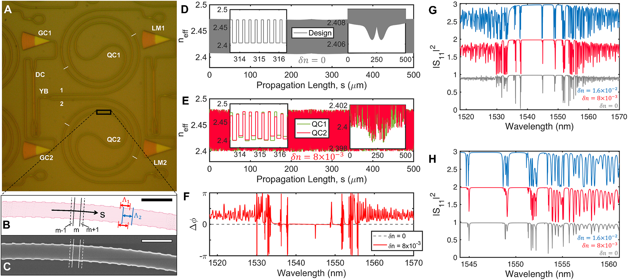
Overview of photonic circuitry and quasicrystal interferometry. (A) Optical microscope image of the integrated silicon photonic QCI PUF architecture. Input/output grating couplers (GC1/GC2), single mode waveguides, and a 50:50 directional coupler (DC) enable pure mode filtering and stable QCI device measurement in transmission. A compact y-branch (YB) splits light into two symmetric arms, (1) and (2), routed to the spiral quasicrystal (QC) arms and loop mirrors (LM1/LM2). (B) Zoomed view of design and (C) SEM image of the curved QC and illustration of the mth segment considered in device modelling (scale bar = 1 μm). (D) Nominal QC effective index profile @ 1550 nm. (E) Example effective index profiles with random errors introduced, and (F) corresponding phase differences between the two arms. (G) Simulated QCI spectra (YB port reflectance) for nominal and random QCIs with varying disorder parameters, and (H) zoomed view of the same.
In our devices, fabrication variations are assumed to primarily stem from local nanoscale variations in waveguide width and surface roughness. To capture the effect of these variations with high sensitivity and visibility, and to not allow them to average out into very few parameters (as in a simple interferometer) or manifest as an ultimately very weak signal (as in waveguide Rayleigh backscatter), it is desirable to create a structure which supports multiple-scattering through the use of many discrete waveguide segments. However, the arrangement of the segments should not have perfect translational symmetry as in a crystal or distributed Bragg reflector (DBR). The properties of a DBR are generally very robust against weak perturbations such as nanoscale disorder owing to destructive interference, with only two narrow windows of enhanced sensitivity near the band edges. The use of linear DBRs instead of our spiral QCs would effectively make the device function like a symmetric single etalon Michaelson Gires–Tournois interferometer (MGTI) [49]. Further, locally breaking the translational symmetry of a DBR in a limited number of locations would effectively yield photonic crystal cavities which only probe disorder in those discrete locations, thus severely limiting the device complexity. Thus, we observe that the use of a QC which entirely lacks translational symmetry (aside from allowed rotational symmetries), naturally arises as a powerful solution to sensitively probing spatially distributed fabrication variations while fostering enhanced complexity.
The arms our QCI PUF consist of width modulated (500 nm ± 20 nm) single mode Si waveguides with nominal device thickness 220 nm cladded by SiO2. The QCs each utilize a slowly varying radius of curvature spiral (R ≈ 50–25 μm), containing 500 µm long multi-periodic Moiré patterned gratings formed by the superposition of gratings with periods Λ1 = 316 nm and Λ2 = 317 nm. Grating teeth (i.e. width equal to 520 nm) are placed at the intersection of Λ1 and Λ2 gratings by performing a Boolean AND function. When considered as a standalone component without disorder, the 1D QC forms longitudinal modes as a result of several effects, which are all related to breaking translational symmetry: (i) the low frequency band edge of the Λ1 grating forms a defect region within the overlapped band gap of the Λ2 grating, (ii) the high frequency band edge of the Λ2 grating forms a defect region within the overlapped band gap of the Λ1 grating, and (iii) additional defect modes are introduced owing to the weak gradual reduction of waveguide effective index with reducing radius of curvature [50]. The output of the QCs are routed to loop mirror (LM)s which offer broadband reflectivity and supports the formation of higher order resonances owing to multi-pass effects. The initial onset of disorder is expected to introduce unique extended states fostering slow-light and resonantly enhanced transmission through the QC in the vicinity of the overlapping fundamental band gaps, while increasing disorder strength should foster the introduction of random localized states and optical resonances exhibiting unique spatial and spectral characteristics. In principle, the exact device design that is used can be flexible, but should ideally provide the following traits: (i) offer high complexity and require numerical methods to model even qualitatively, (ii) support the presence and formation of many spectrally and spatially isolated resonances, (iii) support regions of slow-light effects or high dispersion, (iv) be realized in a regime where fabrication variations constitute a non-negligible fraction of the critical dimensions, and (v) be comprised entirely of weakly modulated single transverse mode waveguides with approximately uniform confinement factors.
The predicted characteristics for QCIs with varying disorder,
In a balanced and lossless interferometer with no phase errors, the reflection spectrum detected from the y-branch should theoretically measure as 100% across the entire spectrum. In our devices however, the waveguides have a finite propagation loss (∼2.4 dB/cm) owing to sidewall roughness and bend loss, as well as passive insertion loss at the interfaces to/from the quasicrystals and loop-mirror y-branches. This loss is significantly enhanced in regions of optical resonance or band edges, becoming a form of coherent perfect loss when critically coupled to quasicrystal or higher order etalon modes [52], [53], and provides distinct features in the spectrum even for a perfectly symmetric and balanced QCI with no disorder,
Regarding environmental stability, it should be emphasized that thermo-optic stimuli can easily perturb a mode frequency
3 Results/Discussion
To experimentally demonstrate our devices, both QCI PUFs and single etalon DBR integrated MGTI reference devices were fabricated in a standard 220 nm device layer SOI platform (see Section 5). Devices were then measured with a tunable laser under TE polarization using the fiber-to-chip grating couplers as illustrated in Figure 2A. The double pass insertion loss of the directional coupler used to probe the QCI sets the minimum on-chip insertion loss to ∼6 dB, rendering the devices easy to measure and align to in an automated testing environment, while the single mode waveguides and single polarization grating couplers render the devices immune to errors in spatial or angular alignment and polarization. To assess the impact of thermal/environmental variation, devices were measured at two temperature settings: setting 1) 23 °C, and setting 2) 30 °C (settings were measured ∼48 h apart from one another). The +7 °C temperature variation mimics the effect of a significant temperature drift which is expected to shift the wavelength for most of the PUF’s spectral features by significantly more than their 3 dB linewidth.
Figure 3A,C shows the measured spectra of three triplicated integrated QCI PUFs (e.g. Figure 2), fabricated in the same process and located next to each other on the same die. The designs of the triplicate structures are all exactly the same with no modifications. However, their optical spectra are entirely unique, effectively serving as a fingerprint for each device. The devices exhibit excellent visibility in grating-coupled transmission, with extinction ratios well in the ∼5–30 dB range.
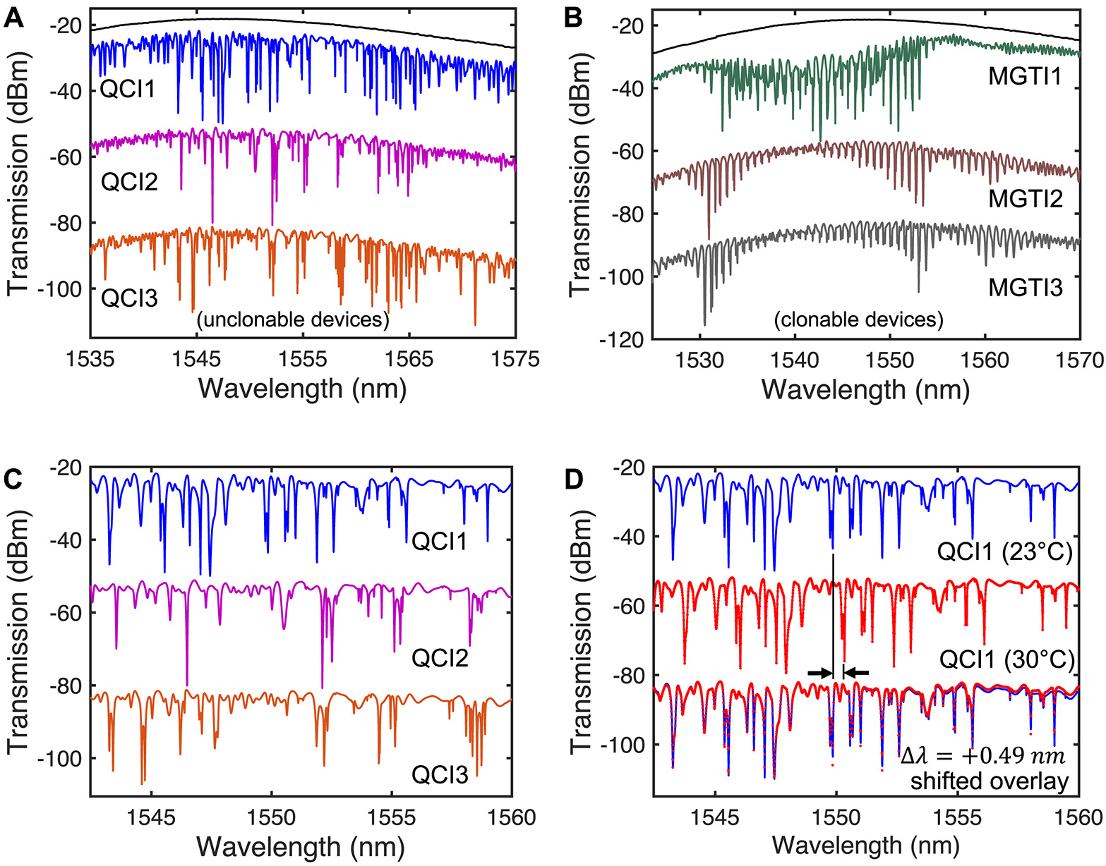
Experimental transmission spectra for triplicated silicon photonic (A) QCI PUFs, and (B) single etalon DBR integrated MGTIs. Black curve corresponds to single pass directional coupler (DC) transmission. Probing of QCIs and MGTIs adds ∼3 dB insertion loss owing to double pass loss through the DC. Device 2/3 spectra are shifted on the y-axis for clarity (C) Zoomed view of QCI PUF spectra showing device uniqueness. (D) Zoomed view of QCI1 spectra at both temperature settings, revealing a deterministic spectral shift.
In the same fabrication run, we also included triplicated single etalon MGTI designs wherein the spiral quasicrystals were replaced with a waveguide delay and simple DBR structure. The DBR length was ∼23 μm with a sidewall grating width modulation of 500 ± 80 nm. The waveguide path length from the y-branch (YB) to the DBR was ∼280 μm and from the DBR to the LM was ∼340 μm. Although the MGTI spectra are ‘randomized’ by fabrication induced phase errors, as visible by the difference in device-to-device spectrum variations from Figure 3B, the device spectra are not unclonable. In the single etalon MGTI devices, an analytical description and exact parameter fit of the device properties could be achieved since the distributed fabrication variations are simply averaged into very few device parameters (i.e. Two values of DBR kappa-L, and four values of optical path lengths, effective/group indices, and optical losses). Over many process runs or iterations, the likelihood of repeating the same MGTI device signature twice (i.e. cloning) becomes very significant despite the randomness imparted into each device. In the QCI PUF device however, the distributed fabrication variations are locally captured in each unique segment of the 1D multiple-scattering waveguide which exponentially increases the device complexity and exponentially suppresses the probability of cloning.
Assuming fabrication errors in a given segment could be simply discretized to five values (i.e. width deviation of ±5 nm in increments of 2.5 nm), the number of device permutations in an MGTI structure with four segments is only on the order of
Figure 3D shows the transmission spectrum for an integrated QCI PUF measured at both temperature settings. All features in the spectral fingerprint of the device near 1550 nm are shifted in wavelength by
As shown in Figure 4, we first performed Hamming distance authentication analysis on the three QCI PUFs. In this computation, each raw spectrum is normalized to the directional coupler reference spectra and then converted to a binary sequence with >10,000 bits. A central subset of 8000 bits is then enrolled and computationally shifted relative to various test keys, at both temperature settings, to search for a match (i.e., Hamming distance <0.3), which is a strong indication of the authenticity. The results confirm the uniqueness of each PUF and validate authentication of each device at both temperature settings.
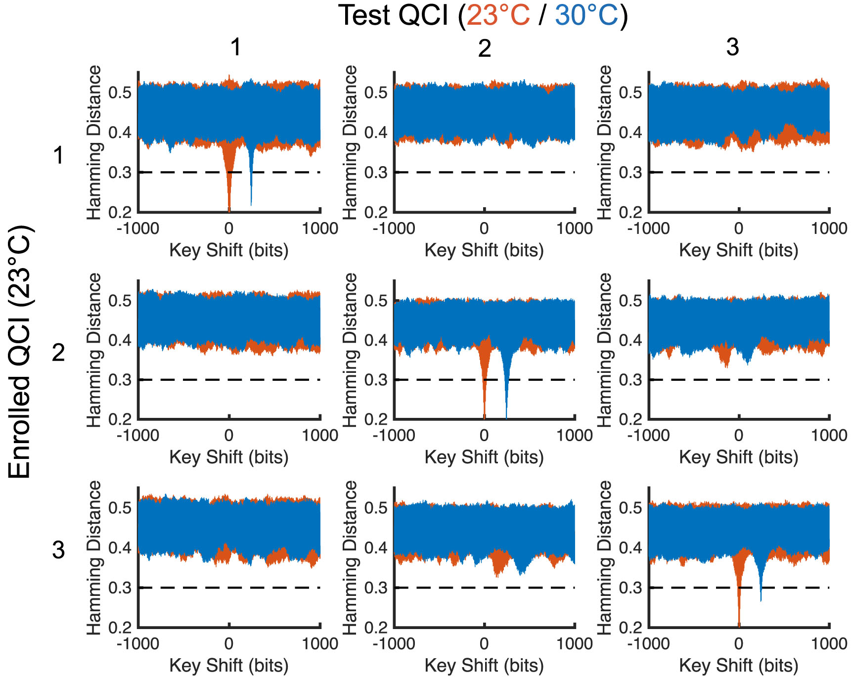
Hamming distance authentication analysis for each silicon photonic QSI PUF at two temperature settings.
In general, directly using the raw output signals of the PUFs for authentication or identification is neither efficient nor robust. To this end, an entropy-harvesting method that can extract chip-unique features will significantly improve the overall performance and functionality of the proposed PUFs and enable scalable identification with large device libraries. The entropy of the spectra of the PUFs generally comes from two sources: inter-chip and intra-chip variations. Inter-chip variations are the intrinsic variations introduced during the fabrication, while intra-chip variations are caused by environmental changes or device aging [9], [57], [58]. Thus, in order to enhance both the uniqueness and reliability of the PUF signature, an ideal entropy-harvesting method should be able to leverage manufacturing process variations, while mitigating intra-chip variations [9], [57], [58], [59], [60]. This includes mitigating any residual probing and/or environmental variations in the grating coupler’s low frequency spectral envelope (Figure 3A) or the PUF’s spectral fingerprint. In our experiments, we applied two types of techniques, i.e., feature extraction and correlation analysis, to illustrate the effectiveness of our integrated photonic PUFs.
For the feature extraction method, we use wavelets to decompose the signal. Figure 5 shows an example of the wavelet decomposition of the raw output signal, s, for QCI1 along with part of the first level of decomposition for all three devices. The best results are observed when we use five-level decompositions (e. g. d5, d4, d3, d2, d1) with Fejer–Korovkin, Symlet, Reverse Biorthogonal wavelets [61] (see Supplementary Information S4). The standard deviation and variance of corresponding sub-bands are then chosen as features. It can be clearly seen from both Figure 5 and Table 1, which illustrates the Fejer–Korovkin derived features, that different devices yield distinct features. As indicated in Table 1, it is observed that the features of the QCI PUFs are stable, since the intra-chip variation is significantly less than the inter-chip variation.
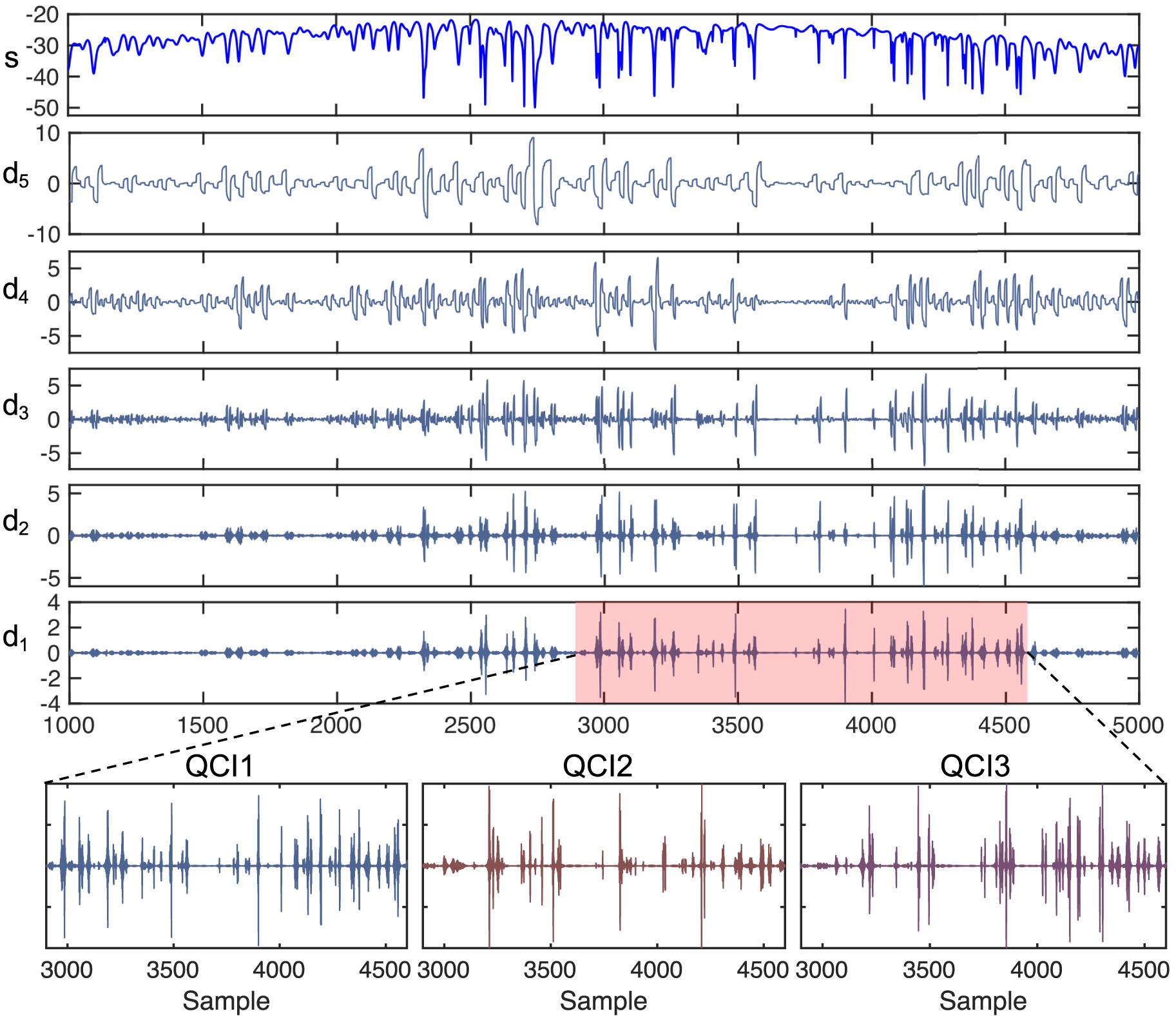
Five-level decomposition of an output signal analyzed by Fejer–Korovkin wavelets. After decomposition, the devices can be distinguished effectively.
Example PUF features extracted from a five-level Fejer–Korovkin wavelet decomposition.
| Device | Setting | Level1 | Level2 | Level3 | Level4 | Level5 |
|---|---|---|---|---|---|---|
| QCI1 | 1 (23 °C) | 0.21 | 1.66 | 7.79 | 30.17 | 119.92 |
| 2 (30 °C) | 0.25 | 1.53 | 7.98 | 30.07 | 106.47 | |
| QCI2 | 1 (23 °C) | 0.14 | 0.73 | 3.98 | 14.26 | 26.16 |
| 2 (30 °C) | 0.10 | 0.84 | 3.57 | 13.30 | 32.24 | |
| QCI3 | 1 (23 °C) | 0.23 | 1.33 | 6.34 | 24.81 | 68.93 |
| 2 (30 °C) | 0.24 | 1.36 | 6.20 | 24.00 | 54.79 |
Device identification can be performed by enrolling the device under test’s features and carrying out an error analysis to identify the device features which yield the lowest mean squared error. Identification can be further strengthened by verifying agreement across different decompositions or complementary techniques such as a power spectral density derived signal correlation. Results for device identification are displayed in Table 2. Correct identification of our QCI PUFs are achieved in all cases, regardless of temperature setting, allowing us to conclude that each PUF will be distinguishable across temperature. For the clonable MGTI devices however, the features are not sufficiently unique and hence different wavelet decompositions mis-identify the enrolled device.
Results of feature extraction and correlation analysis applied to device identification. The “unclonable” QCI PUFs achieve substantial inter-chip variations and are stable across different environmental conditions, while the inter-chip variations of the “clonable” design are not sufficient to identify the enrolled device.
| Device Setting | Unclonable | Clonable | ||||||||||
|---|---|---|---|---|---|---|---|---|---|---|---|---|
| QCI1 | QCI2 | QCI3 | MGTI 1 | MGTI 2 | MGTI 3 | |||||||
| 1 | 2 | 1 | 2 | 1 | 2 | 1 | 2 | 1 | 2 | 1 | 2 | |
| Variance_fk (×102) | 1.6 | 1.16 | 0.01a | Enrolled | 0.3 | 0.1 | 2.41 | 1.8 | 0.01 | ∼0.00a | 0.2 | Enrolled |
| Variance_rbio (×102) | 0.8 | 1.59 | 0 | 0.1 | 0.2 | 0.41 | 0.4a | 1 | 0.76 | 0.5 | ||
| Variance_sym (×102) | 1.5 | 2.04 | 0.01a | 0.2 | 0.3 | 0.96 | 2.1 | 11 | 0.63 | 0.4a | ||
| Correlation | 0.8 | 0.76 | 0.96a | 0.7 | 0.7 | 0.65 | 0.7 | 0.78 | 0.84a | 0.8 | ||
- a
Indicates the identified device for each method.
4 Conclusion
In this work, we introduced and demonstrated photonic circuitry employing single mode TE polarization mode filtering alongside a weakly modulated QCI as a means for realizing a robust PUF. Similar to the original vision of the first optical scattering PUFs, our device probes spatially distributed randomness but realizes it in a highly integrated fashion which is designed to be inherently stable against probing and environmental variations. By comparing our QCI to less complex interferometers, we also experimentally highlighted how randomness is a necessary but not sufficient criterion to achieve unclonable device signatures. We further demonstrated feature extraction as a viable means for optical PUF identification. Since the main source of inter-chip variations are in waveguide width and surface roughness, by precisely analyzing each signal segment within a specific ‘frequency’ domain, and confined ‘time’ domain, it is ensured that these variations are captured during feature extraction and that the most unique features are chosen for the proposed PUFs. Unlike highly multi-mode devices based on chaos, which are extremely sensitive to all conditions, or single-mode optical backscatter which is environmentally stable but extremely weak, the signatures of our device are highly visible, random, and environmentally stable. As a result, our PUF architecture is fully compatible with automated Wafer-scale measurement techniques and fosters scalable implementation within silicon photonic transceivers or photonic systems on a chip as an optical hardware security layer. This work also unveils a new means for amplifying and harnessing the effects of ‘weak’ disorder in photonics – while simultaneously harnessing or constraining specific degrees of freedom – and highlights a viable technological application of quasicrystals and Anderson localized and extended states. Applying the principles of degree of freedom constraints, modal selectivity, and confinement factor control principles, could support the realization of a new generation of disordered photonic systems. In the future, we envision opportunities to further enhance and utilize the functionality of integrated photonic PUFs by leveraging active devices, reconfigurability, multiplexing, far-field signaling, or quantum optics to realize entirely new levels of hardware and information security.
5 Methods
5.1 Modelling
To model the potential characteristics of random silicon photonic PUFs, we developed a transfer matrix model incorporating random parameter variations to derive the complex s-parameters of randomized SBRs with varying degrees of disorder (see Supplementary Information S2). These s-parameters (i.e. amplitude and phase spectra for forward and reverse excitation) are then embedded into a scattering matrix simulator (Lumerical Interconnect) which also accounts for the y-branches, routing waveguides, and LMs.
5.2 Fabrication
Device fabrication and testing was carried out through the Silicon Electronic-Photonic Integrated Circuits program [62]. Structures were fabricated using standard 220 nm SOI via 100 keV electron beam lithography and reactive ion etching at the University of Washington, while automated grating coupled device measurements were performed at The University of British Columbia. A tunable laser (Agilent 81600B) and optical power meter (Agilent 81635A) were used to capture device spectra over the range 1500–1600 nm in 10 pm steps.
Funding source: Air Force Office of Scientific Research (AFOSR)
Award Identifier / Grant number: FA9550-19-1-0057
Funding source: Clemson University
Acknowledgements
This work was supported in part by start-up funds from Clemson University, and the Air Force Office of Scientific Research (AFOSR) under Grant No. FA9550-19-1-0057. We acknowledge the edX UBCx Phot1x Silicon Photonics Design, Fabrication and Data Analysis course organized by Lukas Chrostowski, which is supported by the Natural Sciences and Engineering Research Council of Canada (NSERC) Silicon Electronic-Photonic Integrated Circuits (SiEPIC) Program. The devices were fabricated by Richard Bojko at the Washington Nanofabrication Facility (WNF) at University of Washington, part of the National Science Foundation’s National Nanotechnology Infrastructure Network (NNIN). Hossam Shoman performed the semi-automated optical measurements at The University of British Columbia.
Author contribution: All the authors have accepted responsibility for the entire content of this submitted manuscript and approved submission.
Research funding: The research was funded by Clemson University and the Air Force Office of Scientific Research (AFOSR). SiEPIC is supported by the Natural Sciences and Engineering Research Council of Canada (NSERC).
Conflict of interest statement: The authors are pursuing a patent application, related to this work, with the U.S. Patent and Trademark Office.
References
[1] R. Pappu, B. Recht, J. Taylor, and N. Gershenfeld, “Physical one-way functions,” Science, vol. 297, pp. 2026–2030, 2002, https://doi.org/10.1126/science.1074376.Suche in Google Scholar
[2] B. Gassend, D. Clarke, M. Van Dijk, and S. Devadas, “Silicon physical random functions,” in Proceedings of the 9th ACM Conference on Computer and Communications Security, 2002, pp. 148–160, https://doi.org/10.1145/586110.586132.Suche in Google Scholar
[3] J. D. R. Buchanan, R. P. Cowburn, A. V. Jausovec, et al., “‘Fingerprinting’ documents and packaging,” Nature, vol. 436, p. 475, 2005, https://doi.org/10.1038/436475a.Suche in Google Scholar
[4] U. Rührmair, C. Hilgers, S. Urban, “Revisiting optical physical unclonable functions,” IACR Cryptology ePrint Archive, vol. 215, 2013, http://citeseerx.ist.psu.edu/viewdoc/download?doi=10.1.1.301.2374&rep=rep1&type=pdf.Suche in Google Scholar
[5] Y, Gao, S. F. Al-Sarawi, D, Abbott, “Physical unclonable functions,” Nature Electronics, vol. 3, pp. 81–91, 2020. https://doi.org/10.1038/s41928-020-0372-5.10.1038/s41928-020-0372-5Suche in Google Scholar
[6] A. Uchida, K. Amano, M. Inoue, et al., “Fast physical random bit generation with chaotic semiconductor lasers,” Nat. Photon., vol. 2, p. 728, 2008, https://doi.org/10.1038/nphoton.2008.227.Suche in Google Scholar
[7] C. S. Pétrie, J. Alvin Connelly, “A noise-based ic random number generator for applications in Cryptography,” IEEE Trans. Circ. Syst. Fund. Theor. Appl., vol. 47, no. 5, pp. 615–621, 2000. https://doi.org/10.1109/81.847868.Suche in Google Scholar
[8] R. S. Indeck and E. Glavinas, “Fingerprinting magnetic media,” IEEE Trans. Magn., vol. 29, pp. 4095–4097, 1993, https://doi.org/10.1109/20.281401.Suche in Google Scholar
[9] Y. Lao, B. Yuan, C. H. Kim, K. K. Parhi, “Reliable PUF-based local authentication with self-correction,” IEEE Trans. Comput. Aided Des. Integrated Circ. Syst., vol. 36, no. 2, pp. 201–213, 2017. https://doi.org/10.1109/TCAD.2016.2569581.Suche in Google Scholar
[10] P. Prabhu, A. Akel, L. M. Grupp, et al., “Extracting device fingerprints from flash memory by exploiting physical variations,” in Lecture Notes in Computer Science (including subseries Lecture Notes in Artificial Intelligence and Lecture Notes in Bioinformatics), 2011, https://doi.org/10.1007/978-3-642-21599-5_14.Suche in Google Scholar
[11] B. C. Grubel, B. T. Bossworth, M. R. Kossey, A. B. Cooper, M. A. Foster, and A. C. Foster, “Secure communications using nonlinear silicon photonic keys,” Optic Express, vol. 26, p. 4710, 2018, https://doi.org/10.1364/OE.26.004710.Suche in Google Scholar
[12] A. Di Falco, V. Mazzone, A. Cruz, and A. Fratalocchi, “Perfect secrecy cryptography via mixing of chaotic waves in irreversible time-varying silicon chips,” Nat. Commun., vol. 10, p. 5827, 2019, https://doi.org/10.1038/s41467-019-13740-y.Suche in Google Scholar
[13] T. McGrath, I. E. Bagci, Z. M. Wang, U. Roedig, R. J. Young, “A PUF taxonomy,” Appl. Phys. Rev., vol. 6, p. 011303, 2019. https://doi.org/10.1063/1.5079407.Suche in Google Scholar
[14] C. Chang, Y. Zheng, and L. Zhang, “A Retrospective and a look forward: fifteen years of physical unclonable function advancement,” IEEE Circuits Syst. Mag., vol. 17, pp. 32–62, 2017, https://doi.org/10.1109/MCAS.2017.2713305.Suche in Google Scholar
[15] Y. Lao, K. K. Parhi, “Statistical analysis of MUX-based physical unclonable functions,” IEEE Trans. Comput. Aided Des. Integrated Circ. Syst., vol. 33, no. 5, pp. 649–662, 2014. https://doi.org/10.1109/TCAD.2013.2296525.Suche in Google Scholar
[16] M. Bhargava, C. Cakir, and K. Mai, “Reliability enhancement of bi-stable PUFs in 65nm bulk CMOS,” in Proceedings of the 2012 IEEE International Symposium on Hardware-Oriented Security and Trust, HOST 2012, 2012, https://doi.org/10.1109/HST.2012.6224314.Suche in Google Scholar
[17] Y. Cao, L. Zhang, S. S. Zalivaka, C. H. Chang, and S. Chen, “CMOS image sensor based physical unclonable function for coherent sensor-level authentication,” IEEE Trans. Circ. Syst. I. Regul. Pap., vol. 62, pp. 2629–2640, 2015, https://doi.org/10.1109/TCSI.2015.2476318.Suche in Google Scholar
[18] R. Arppe and T. J. Sørensen, “Physical unclonable functions generated through chemical methods for anti-counterfeiting,” Nat. Rev. Chem., vol. 1, p. 31, 2017, https://doi.org/10.1038/s41570-017-0031.Suche in Google Scholar
[19] J. Roberts, I. E. Bagci, M. A. Zawawi, et al., “Using quantum confinement to uniquely identify devices,” Sci. Rep., vol. 5, pp. 1–8, 2015, https://doi.org/10.1038/srep16456.Suche in Google Scholar
[20] Z. Hu, J. M. Comeras, H. Park, et al., “Physically unclonable cryptographic primitives using self-assembled carbon nanotubes,” Nat. Nanotechnol., vol. 11, pp. 559–565, 2016, https://doi.org/10.1038/nnano.2016.1.Suche in Google Scholar
[21] A. Alharbi, D. Armstrong, S. Alharbi, and D. Shahrjerdi, “Physically unclonable cryptographic primitives by chemical vapor deposition of layered MoS2,” ACS Nano, vol. 11, pp. 12772–12779, 2017, https://doi.org/10.1021/acsnano.7b07568.Suche in Google Scholar
[22] A. F. Smith, P. Patton, and S. E. Skrabalak, “Plasmonic nanoparticles as a physically unclonable function for responsive anti-counterfeit nanofingerprints,” Adv. Funct. Mater., vol. 26, pp. 1315–1321, 2016, https://doi.org/10.1002/adfm.201503989.Suche in Google Scholar
[23] H. Chen, M. Song, Z. Guo, et al., “Highly secure physically unclonable cryptographic primitives based on interfacial magnetic anisotropy,” Nano Lett., vol. 18, pp. 7211–7216, 2018, https://doi.org/10.1021/acs.nanolett.8b03338.Suche in Google Scholar
[24] A. Dodda, A. Wali, Y. Wu, et al., “Biological one-way functions for secure key generation,” Adv. Theory Simul., vol. 2, 2019, Art no. 1800154, https://doi.org/10.1002/adts.201800154.Suche in Google Scholar
[25] D. Wiersma, “The smallest random laser,” Nature, vol. 406, pp. 133–135, 2000, https://doi.org/10.1038/35018184.Suche in Google Scholar
[26] S. A. Goorden, M. Horstmann, A. P. Mosk, B. Škorić, and P. W. H. Pinkse, “Quantum-secure authentication of a physical unclonable key,” Optica, vol. 1, pp. 421–424, 2014, https://doi.org/10.1364/OPTICA.1.000421.Suche in Google Scholar
[27] B. T. Bosworth, I. A. Atakhodjaev, M. R. Kossey, et al., “Unclonable photonic keys hardened against machine learning attacks,” APL Photon., vol. 5, p. 10803, 2020, https://doi.org/10.1063/1.5100178.Suche in Google Scholar
[28] C. Helfmeier, C. Boit, D. Nedospasov, and J.-P. Seifert, “Cloning physically unclonable functions,” in 2013 IEEE International Symposium on Hardware-Oriented Security and Trust (HOST), vol. 1–6, IEEE, 2013.10.1109/HST.2013.6581556Suche in Google Scholar
[29] U. Rührmair, J. Sölter, F. Sehnke, et al., “PUF modeling attacks on simulated and silicon data,” IEEE Trans. Inf. Forensics Secur., vol. 8, pp. 1876–1891, 2013, https://doi.org/10.1109/tifs.2013.2279798.Suche in Google Scholar
[30] Y. Xu, W. Liu, Y. Lao, Z. Zhang, X. You, C. Zhang, “Mathematical modeling analysis of strong physical unclonable functions,” IEEE Trans. Comput. Aided Des. Integrated Circ. Syst., vol. 1, 2020, https://doi.org/10.1109/TCAD.2020.2969645.Suche in Google Scholar
[31] C. Mesaritakis, M. Akriotou, A. Kapsalis, et al., “Physical unclonable function based on a multi-mode optical waveguide,” Sci. Rep., vol. 8, pp. 1–12, 2018, https://doi.org/10.1038/s41598-018-28008-6.Suche in Google Scholar
[32] B. C. Grubel, B. T. Bosworth, M. R. Kossey, et al., “Silicon photonic physical unclonable function,” Optic Express, vol. 25, p. 12710, 2017, https://doi.org/10.1364/OE.25.012710.Suche in Google Scholar
[33] B. C. Grubel, D. S. Vresilovic, B. T. Bosworth, et al., “Light transport through ultrafast chaotic micro-cavities for photonic physical unclonable functions,” 2017 51st Annual Conference on Information Sciences and Systems (CISS), vol. 2017, 2017, pp. 1–6, https://doi.org/10.1109/CISS.2017.7926067.Suche in Google Scholar
[34] D. S. Wiersma, “The physics and applications of random lasers,” Nat. Phys., vol. 4, p. 359, 2008, https://doi.org/10.1038/nphys971.Suche in Google Scholar
[35] S. T. Kreger, D. K. Gifford, M. E. Froggatt, B. J. Soller, M. S. Wolfe, “High resolution distributed strain or temperature measurements in single-and multi-mode fiber using swept-wavelength interferometry,”. Optical Fiber Sensors OSA Technical Digest, paper ThE42. Optical Society of America; 2006. https://doi.org/10.1364/OFS.2006.ThE42.Suche in Google Scholar
[36] M. E. Froggatt and D. K. Gifford, “Rayleigh backscattering signatures of optical fibers—their properties and applications,” in 2013 Optical Fiber Communication Conference and Exposition and the National Fiber Optic Engineers Conference (OFC/NFOEC), vol. 1–3, 2013.10.1364/OFC.2013.OW1K.6Suche in Google Scholar
[37] A. H. Atabaki, S. Moazeni, F. Pavanello, et al., “Integrating photonics with silicon nanoelectronics for the next generation of systems on a chip,” Nature, vol. 556, pp. 349–354, 2018, https://doi.org/10.1038/s41586-018-0028-z.Suche in Google Scholar
[38] R. Jones, P. Doussiere, J. B. Driscoll, et al., “Heterogeneously integrated InP/Silicon photonics: fabricating fully functional transceivers,” IEEE Nanotechnol. Mag., vol. 13, pp. 17–26, 2019, https://doi.org/10.1109/MNANO.2019.2891369.Suche in Google Scholar
[39] C. Torrence, G. P. Compo, “A practical guide to wavelet analysis,” Bull. Am. Meteorol. Soc., vol. 79, pp. 61–78, 1998. https://doi.org/10.1175/1520-0477(1998)079<0061:APGTWA>2.0.CO;2.10.1175/1520-0477(1998)079<0061:APGTWA>2.0.CO;2Suche in Google Scholar
[40] A. Phinyomark, C. Limsakul, P. Phukpattaranont, “Application of wavelet analysis in EMG feature extraction for pattern classification,” Meas. Sci. Rev., vol. 11, no. 2, pp. 45–52, 2011. https://doi.org/10.2478/v10048-011-0009-y.Suche in Google Scholar
[41] Y. Wang, X. Wang, J. Flueckiger, et al., “Focusing sub-wavelength grating couplers with low back reflections for rapid prototyping of silicon photonic circuits,” Opt. Express, vol. 22, pp. 20652–20662, 2014, https://doi.org/10.1364/OE.22.020652.Suche in Google Scholar
[42] E. Dulkeith, F. N. Xia, L. Schares, W. M. J. Green, and Y. A. Vlasov, “Group index and group velocity dispersion in silicon-on-insulator photonic wires,” Optic Express, vol. 14, p. 3853, 2006, https://doi.org/10.1364/OE.14.003853.Suche in Google Scholar
[43] M. Davy, and A. Z. Genack, “Selectively exciting quasi-normal modes in open disordered systems,” Nat. Commun., vol. 9, p. 4714, 2018, https://doi.org/10.1038/s41467-018-07180-3.Suche in Google Scholar
[44] M. Segev, Y. Silberberg, and D. N. Christodoulides, “Anderson localization of light,” Nat. Photon., vol. 7, pp. 197–204, 2013, https://doi.org/10.1038/nphoton.2013.30.Suche in Google Scholar
[45] G. Roati, C. D’Errico, L. Fallani, et al., “Anderson localization of a non-interacting Bose–Einstein condensate,” Nature, vol. 453, pp. 895–898, 2008, https://doi.org/10.1038/nature07071.Suche in Google Scholar
[46] M. Ghulinyan, C. J. Oton, L. Dal Negro, et al., “Light-pulse propagation in Fibonacci quasicrystals,” Phys. Rev. B Condens. Matter, vol. 71, 2005, https://doi.org/10.1103/PhysRevB.71.094204.Suche in Google Scholar
[47] L. Levi, M. Rechtsman, B. Freedman, T. Schwartz, O. Manela, and M. Segav, “Disorder-enhanced transport in photonic quasicrystals,” Science, vol. 332, pp. 1541–1544, 2011, https://doi.org/10.1126/science.1202977.Suche in Google Scholar
[48] P, Wang, Y, Zheng, X, Chen, et al., “Localization and delocalization of light in photonic moiré lattices,” Nature, vol. 577, no. 7788, pp. 42–46, 2020. https://doi.org/10.1038/s41586-019-1851-6.Suche in Google Scholar
[49] B. B. Dingel and M. Izutsu, “Multifunction optical filter with a Michelson–Gires–Tournois interferometer for wavelength-division-multiplexed network system applications,” Opt. Lett., vol. 23, pp. 1099–1101, 1998, https://doi.org/10.1364/ol.23.001099.Suche in Google Scholar
[50] A. D. Simard, Y. Painchaud, and S. LaRochelle, “Integrated Bragg gratings in spiral waveguides,” Optic Express, vol. 21, pp. 8953–8963, 2013, https://doi.org/10.1364/oe.21.008953.Suche in Google Scholar
[51] B. Wang, S, Mazoyer, J. P Hugonin, P, Lalanne, “Backscattering in monomode periodic waveguides,” Phys. Rev. B., vol. 78, p. 245108, 2008. https://doi.org/10.1103/PhysRevB.78.245108.Suche in Google Scholar
[52] R. R. Grote, J. B. Driscoll, and R. M. Osgood, “Integrated optical modulators and switches using coherent perfect loss,” vol. 38, pp. 3001–3004, 2013, https://doi.org/10.1364/ol.38.003001.Suche in Google Scholar
[53] J. D. Ryckman, “Random coherent perfect absorption with 2d atomic materials mediated by Anderson localization,” ACS Photonics, vol. 5, no. 2, pp. 574–580, 2018. https://doi.org/10.1021/acsphotonics.7b01135.Suche in Google Scholar
[54] B. Redding, S. Fatt Liew, Y. Bromberg, R. Sarma, and H. Cao, “Evanescently coupled multimode spiral spectrometer,” Optica, vol. 3, p. 956, 2016, https://doi.org/10.1364/OPTICA.3.000956.Suche in Google Scholar
[55] B. Redding, S. F. Liew, R. Sarma, and H. Cao, “Compact spectrometer based on a disordered photonic chip,” Nat. Photon., vol. 7, p. 746, 2013, https://doi.org/10.1038/nphoton.2013.190.Suche in Google Scholar
[56] H. Cao, “Lasing in random media,” Waves Random Media, vol. 13, pp. R1–R39, 2003, https://doi.org/10.1088/0959-7174/13/3/201.Suche in Google Scholar
[57] G. E. Suh and S. Devadas, “Physical unclonable functions for device authentication and secret key generation,” in Proceedings - Design Automation Conference, 2007, https://doi.org/10.1109/DAC.2007.375043.Suche in Google Scholar
[58] C. Herder, M. D. Yu, F. Koushanfar, and S. Devadas, “Physical unclonable functions and applications: a tutorial,” Proc. IEEE, vol. 102, pp. 1126–1141, 2014, https://doi.org/10.1109/JPROC.2014.2320516.Suche in Google Scholar
[59] C. E. Yin and G. Qu, “Temperature-aware cooperative ring oscillator puf,” in 2009 IEEE International Workshop on Hardware-Oriented Security and Trust, HOST 2009, 2009, https://doi.org/10.1109/HST.2009.5225055.Suche in Google Scholar
[60] K. Yang, Q. Dong, D. Blaauw, and D. Sylvester, “A physically unclonable function with BER <10-8 for robust chip authentication using oscillator collapse in 40nm CMOS,” in Digest of Technical Papers - IEEE International Solid-State Circuits Conference, 2015, https://doi.org/10.1109/ISSCC.2015.7063022.Suche in Google Scholar
[61] A. Graps, “An Introduction to wavelets,” IEEE Comput. Sci. Eng., vol. 2, pp. 50–61, 1995, https://doi.org/10.1109/99.388960.Suche in Google Scholar
[62] L. Chrostowski, H. Shoman, M. Hammood, et al., “Silicon photonic circuit design using rapid prototyping foundry process design kits,” IEEE J. Sel. Top. Quantum Electron., vol. 25, pp. 1–26, 2019, https://doi.org/10.1109/jstqe.2019.2917501.Suche in Google Scholar
Supplementary material
The online version of this article offers supplementary material (https://doi.org/10.1515/nanoph-2020-0049).
© 2020 Farhan Bin-Tarik et al., published by De Gruyter, Berlin/Boston
This work is licensed under the Creative Commons Attribution 4.0 International License.
Artikel in diesem Heft
- Reviews
- Low-dimensional saturable absorbers for ultrafast photonics in solid-state bulk lasers: status and prospects
- Recent progress on applications of 2D material-decorated microfiber photonic devices in pulse shaping and all-optical signal processing
- Superconducting nanowire single-photon detectors for quantum information
- Light-field and spin-orbit-driven currents in van der Waals materials
- Active photonic platforms for the mid-infrared to the THz regime using spintronic structures
- Dynamics of carbon nanotube-based mode-locking fiber lasers
- Research Articles
- 164 fs mode-locked erbium-doped fiber laser based on tungsten ditelluride
- Convolution operations on time-domain digital coding metasurface for beam manipulations of harmonics
- Tellurene-based saturable absorber to demonstrate large-energy dissipative soliton and noise-like pulse generations
- Controllable all-optical modulation speed in hybrid silicon-germanium devices utilizing the electromagnetically induced transparency effect
- Simultaneous field enhancement and loss inhibition based on surface plasmon polariton mode hybridization
- Robust optical physical unclonable function using disordered photonic integrated circuits
- Broadband and high-efficiency accelerating beam generation by dielectric catenary metasurfaces
- Broadband photonic topological insulator based on triangular-holes array with higher energy filling efficiency
- 3D super-resolved imaging in live cells using sub-diffractive plasmonic localization of hybrid nanopillar arrays
- Real-time terahertz meta-cryptography using polarization-multiplexed graphene-based computer-generated holograms
- Thermal-responsive multicolor emission of single NaGdF4:Yb/Ce/Ho upconversion nanocrystals for anticounterfeiting application
- Yttrium oxide as a Q-switcher for the near-infrared erbium-doped fiber laser
- High-quality micropattern printing by interlacing-pattern holographic femtosecond pulses
- End-emitting nano organic light emitting diodes (OLEDs) with directional output
- Multiphysical sensing of light, sound and microwave in a microcavity Brillouin laser
- Ultra-wideband enhancement on mid-infrared fingerprint sensing for 2D materials and analytes of monolayers by a metagrating
- Microcavity-coupled emitters in hexagonal boron nitride
- Exploiting deep learning network in optical chirality tuning and manipulation of diffractive chiral metamaterials
- Time-varying optical vortices enabled by time-modulated metasurfaces
- Direct routing of intensity-editable multi-beams by dual geometric phase interference in metasurface
- Fabrication of highly uniform nanoprobe via the automated process for tip-enhanced Raman spectroscopy
- Ultra-thin curved visible microdisk lasers with three-dimensional whispering gallery modes
- Spatial multiplexing holographic combiner for glasses-free augmented reality
- Terahertz plasmonic phase-jump manipulator for liquid sensing
- Facile sonochemical-assisted synthesis of orthorhombic phase black phosphorus/rGO hybrids for effective photothermal therapy
- Facile integration of MoS2/SiC photodetector by direct chemical vapor deposition