
Plasmonic nanofocusing spectral interferometry
-
Martin Esmann
 ,
Abbas Chimeh
,
Abbas Chimeh


Abstract
We describe and demonstrate a novel experimental approach to measure broadband, amplitude- and phase-resolved scattering spectra of single nanoparticles with 10-nm spatial resolution. Nanofocusing of surface plasmon polaritons (SPPs) propagating along the shaft of a conical gold taper is used to create a spatially isolated, spectrally broad nanoscale light source at its very apex. The interference between these incident SPPs and SPPs that are backpropagating from the apex leads to the formation of an inherently phase-stable interferogram, which we detect in the far field by partially scattering SPPs off a small protrusion on the taper shaft. We show that these interferograms allow the reconstruction of both the amplitude and phase of the local optical near fields around individual nanoparticles optically coupled to the taper apex. We extract local light scattering spectra of particles and quantify line broadenings and spectral shifts induced by tip-sample coupling. Our experimental findings are supported by corresponding finite-difference time-domain and coupled dipole simulations and show that, in the limit of weak tip-sample coupling, the measurements directly probe the projected local density of optical states of the plasmonic system. The combination of a highly stable inline interferometer with the inherent optical background suppression through nanofocusing makes it a promising tool for the locally resolved study of the spectral and temporal optical response of coupled hybrid nanosystems.
1 Introduction
The electronic local density of states, which represents the number of electronic states in a certain volume and energy interval, is one of the most fundamental quantities in nanoscience. Its exploration by scanning tunneling microscopy (STM) has led to intriguing studies of quantum corrals [1], [2] and many-body phenomena such as quantum mirages [3], [4]. In plasmonic and photonic nanostructures, the corresponding quantity is the electromagnetic local density of states (LDOS), i.e. the electromagnetic field – created by the structure after excitation by a point-like isotropic source – at the position of the source [5], [6]. It is of immediate relevance for controlling the spontaneous emission of quantum emitters by their nanostructured environment [7]. The related projected LDOS measures the polarization component of the field at the source position, which is induced by a linearly polarized point source and pointing along this direction. Because of its importance for designing optical properties at the nanoscale, experimental LDOS studies have received substantial attention [8], [9], [10], [11], [12], [13], [14], [15].
Conceptually, a straightforward approach towards LDOS mapping is scanning near-field optical microscopy (SNOM), in which a pointed tip senses the local electromagnetic field near the surface of a sample. A quantitative interpretation of near-field images and a direct relation of these images to LDOS maps, however, turn out to be quite challenging, in particular in the visible and near-infrared region of the electromagnetic spectrum [16], [17], [18]. This is not only due to the complex vectorial properties of the optical near fields of photonic and plasmonic nanostructures [19], [20], [21], [22] but more fundamentally due to the challenge in creating a point-like and spatially isolated light source with a spectrum that is sufficiently broad to excite the relevant optical resonances of the sample. A second important aspect is the inherent near-field coupling between the tip and the sample [23], [24]. In general, this makes the SNOM tip a perturbative probe of the local optical near field [17], [18], [25], [26] unless multiple reflections between the tip and the sample can be safely neglected [26] for sufficiently large tip-sample distances.
As a consequence, electron-based spectroscopy techniques, in particular electron energy loss spectroscopy (EELS) and cathodoluminescence (CL) spectroscopy, are becoming increasingly important for LDOS imaging [27], [28], [29] ever since Nelayah et al. demonstrated that EELS can probe the modes of plasmonic nanoparticles with exquisite spatial resolution [30]. Theoretically, the image contrast in EELS probing the work done on a swift electron by the electric field that is emitted from a nanostructure after it has been impulsively excited by the field of the electron is well understood [31], [32]. It has been shown that the probability that a swift electron loses a quantum of energy to the material excitation is equivalent to the projection of the LDOS of the nanostructure along the trajectory of the electron [31], [33], [34]. Complementary to EELS, CL [34], [35] probes the electron-induced far-field radiation and provides the projection of the radiative LDOS on the electron trajectory.
Even though EELS is such an established and powerful technique for probing the projected LDOS of plasmonic nanostructures, it has, in its present implementation, certain evident limitations. Apart from its specific momentum selection rules [36], the energy resolution is restricted to the 10-meV range, despite significant progress in monochromator design [37], [38]. Also, dynamic studies of the LDOS with a time resolution below the 10-fs lifetime of the relevant surface plasmon (SP) excitation are currently out of reach. In principle, both these limitations may be overcome by SNOM techniques [39], which makes it interesting to reconsider the use of SNOM for LDOS imaging. Progress in this direction has recently been achieved by using plasmonic nanofocusing [40], [41], [42] to create a spatially isolated, spectrally broadband, and background-free nanometer-sized light spot [43], [44], [45], [46], [47], [48] with well-controlled polarization properties [49] at the very apex of a sharp conical gold taper. Radially polarized surface plasmon polariton (SPP) waves that are coupled to the shaft of such a taper are nanofocused to its apex. The integration of such a plasmonic nanofocusing probe into an atomic force microscope (AFM) [42], [43], [44], [50] or an STM [51], [52] can selectively bring this optical excitation to a specific point near the sample surface, making it an effective tool for spatially resolved studies of light-matter interaction at the nanoscale. Most recently [26], such a light source has been used to record local light scattering spectra from single gold nanorods with 5-nm spatial resolution. These plasmonic nanofocusing spectra (PNS) provided quantitative insight into near-field couplings between the tip and the nanorod and highlighted in particular the role of the anisotropic tip polarizability in the tip-sample interaction. The recorded light scattering spectra, however, showed rather complex Fano-like spectral line shapes [26], resulting from the interference between fields emitted by the nanorod sample and the tip. This complicated an immediate interpretation of the local scattering spectra. For a more direct measurement of the LDOS of the investigated nanostructure, it seems desirable to solely detect the optical near field at the tip position and to avoid interference between the fields scattered from multiple sources.
Here, we describe and implement a new experimental technique, called plasmonic nanofocusing spectral interferometry (PNSI), to locally excite and detect near-field scattering spectra of single nanostructures. SPP waves are nanofocused to the apex of a sharp conical gold taper and used to locally excite single gold nanorods. The optical near fields that are emitted by the nanorods couple back to the apex and launch backpropagating SPP waves at the taper. Interference with incident SPP waves results in an inherently phase-stable spectral interferogram (SI), which allows sensitive measurement of both the amplitude and phase of the electric field around a single nanorod with <10 nm spatial resolution over a broad spectral range. We show that the use of the radially symmetric guided mode of the taper [49] for both excitation and collection of optical near fields allows, in the limit of sufficiently weak tip-sample coupling, the quantitative mapping of the projected LDOS of the nanostructured sample.
2 Results
Experimentally, we generate a spatially isolated dipole scatterer at the apex of a gold nanotaper by nanofocusing SPPs propagating along its shaft. As shown in Figure 1A, broadband laser radiation (650–900 nm, ~300 μW incident power) is focused onto a grating coupler that is placed 50 μm above the apex, launching a coherent superposition of radially polarized SPP modes with different angular momenta m [29], [53]. All higher order modes (|m|>0) are coupled to far-field radiation at a distance of at least hundreds of nanometers from the apex [54]. Only the lowest order, rotationally symmetric taper mode with angular momentum m=0 is nanofocused at the apex with a radius of 9 nm [40], [54]. There it creates a localized electromagnetic field which is reasonably similar to that generated by an isolated point dipole moment, pt, located in the apex center rt and oriented along the taper axis z [49]. The spectral distribution of this light spot is basically given by the grating-coupled fraction of the incident laser. We use this bright, spectrally broad, and spatially isolated nano light source to locally excite and probe the near fields of the localized surface plasmon (LSP) modes of 40 nm×10 nm×10 nm sized gold nanorods that are placed at the surface of a thin glass sheet. Importantly, the nanofocusing not only leads to the generation of near and far fields in the vicinity of the tip apex. The field created by the z-component pt,z of the tip dipole moment couples to the m=0 mode and launches an SPP field that is backpropagating along the taper shaft. All other polarization components of pt create nonpropagating fields since the re-emitted field profile does not match that of the nanofocused m=0 mode. As long as the tip is far away from the sample surface, the backpropagating field is mainly given by the partial reflections of the nanofocused SPP field E0(ω, rt). When the tip approaches the sample, the nanofocused light spot induces an optical polarization in the sample, and the fields Er that are re-emitted by the sample can couple back to the tip apex. As such, they will modify the tip dipole moment pt and thus the backpropagating SPP field. Because of the radial polarization of the m=0 mode, this secondary backpropagating field is directly proportional to the z-component of the total electric field at the apex: Ea(ω, rt)=E0(ω, rt)+Er(ω, rt). It thus allows selective readout of Ea,z=E0,z+Er,z at the tip apex location, thus avoiding any mixing with the fields generated at other locations upon exciting the sample. Experimentally, we locally probe the forward- and backward-propagating SPP fields by collecting the far-field scattering from small, isolated scatterers on the shaft with ~100 nm diameter. These scatterers are small (gold) precipitates that are naturally formed at very low density during the etching process (right inset in Figure 1A). From three such point-like scatterers (S1–S3) located at distances between 3 and 14 μm from the taper apex (Figure 1B), we collect scattering spectra through a microscope objective, providing a spatial resolution of ~2 μm. This is sufficient to isolate an individual scatterer at the tip shaft. The collected spectra display pronounced spectral modulations (Figure 1C). The fringe spacing and fringe contrast both gradually decrease with increasing distance. These SIs [55], [56], [57], [58] reflect the interference between the grating-coupled SPP field that is incident on the protrusion and scattered towards the detector (E1) and the backpropagating SPP field that is coupled into the far field (E2). The SI, S(ω)=|E1(ω)+E2(ω)|2, thus probes the interference between the incident field Es1 and the backpropagating SPP field Es2 at the position of the scatterer. The fringe spacing Δω=2π/τ0 is a measure of the time delay, τ0=2L/cSPP, acquired by the SPP wave upon propagation from the scatterer to the tip apex and back. Comparing the tip-scatterer distances L of 3.1, 7.7, and 13.7 μm deduced from optical microscopy images with the respective fringe spacings in Figure 1C, we infer an average SPP group velocity of cSPP=(0.94±0.06)c0 (c0: speed of light in vacuum). The fringe contrast in the SI from S1 suggests that the backreflected SPP amplitude is at most 30% smaller than the incident amplitude. The decrease in amplitude with distance points to a spectrally averaged SPP propagation length of at least 14 μm on the taper shaft. If the tip is positioned far away from the surface or on a sample region without nanoparticles, the backreflected spectrum is very similar to the incident laser spectrum. In contrast, when positioning the tip near the apices of one of the gold nanorods, also the field Er,z emitted by exciting the longitudinal LSP resonance of the nanorod, centered around 1.55 eV with a line width of 50–100 meV, contributes to the backpropagating SPP field and, thus, to the SI. Both the amplitude (black open circles in Figure 1D) and spectral phase (red open circles) of the LSP spectrum can be extracted from a Fourier analysis of the SI. The retrieved spectrum shows an absorptive line shape, with amplitude and spectral phase well described by a Lorentzian line shape model with a resonance energy of 1.551 eV and a full width at half-maximum 2ℏγ=0.14 eV (solid lines).
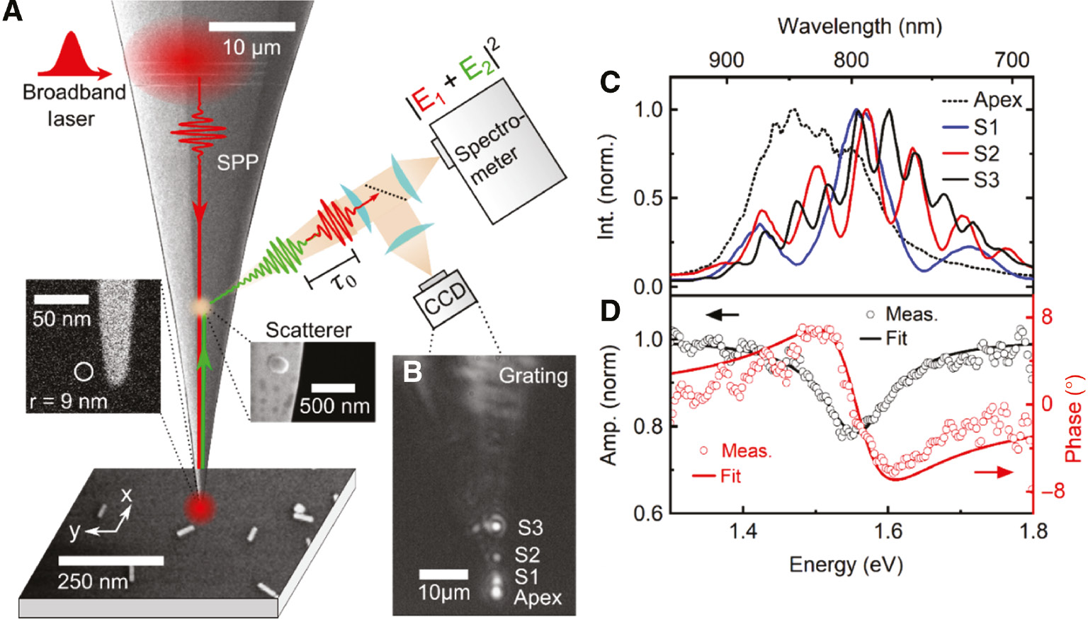
Plasmonic nanofocusing spectral interferometry (PNSI) of individual gold nanorods.
(A) Broadband laser radiation is grating-coupled to SPPs on the shaft of a conical gold taper. The SPPs are nanofocused to a 10-nm-sized light source at its apex (left inset), locally exciting individual gold nanorods. The field emitted by the nanorod couples back to the apex, launching a secondary, backpropagating SPP field (green arrow). Protrusions of ~100 nm size on the shaft (right inset) scatter both the incident SPP field E1 and the time-delayed backpropagating field E2 into the far field, generating a spectral interferogram (SI) on the detector. (B) Side view of the gold taper showing light scattering from the apex and three additional scatterers (S1–S3). (C) SIs recorded by selectively collecting the light scattered from S1, S2, and S3, together with the apex spectrum (dashed line). The spectra from the scatterers show a pronounced spectral modulation with a fringe spacing that decreases with the apex-scatterer distance, i.e. with increasing time delay τ0 between E1 and E2. (D) Amplitude (black open symbols) and phase spectrum (red open symbols) of a gold nanorod reconstructed from the SI. The longitudinal surface plasmon resonance at 1.56 eV is shown, together with fits to a Lorentzian line shape function (solid lines).
We use a two-step strategy, illustrated in Figure 2, to retrieve the field Er,z from these interferograms. To validate our approach, the same evaluation method has been applied to a simulated SI (see Figure S1) and is shown to retrieve the nanorod spectrum with high fidelity. We first measure a reference interferogram from scatterer S3 by placing the tip on the bare glass substrate (red dashed line in Figure 2A) and then compare this to the SI from the same scatterer when the tip is close to the apex of a gold nanorod (black line, recorded at position D in Figure 3A). Both spectra show pronounced interferences, with the same modulation frequency throughout the range of the laser spectrum. In the difference between these two spectra (Figure 2B), the interference fringes are restricted to a narrower region around the LSP resonance. This difference spectrum reflects the modification of the backpropagating field Es2 due to the fields that are emitted by the nanorod. To reconstruct these fields, we perform a Fourier transformation of the SI into the time domain (Figure 2C). Expressing the backpropagating field as
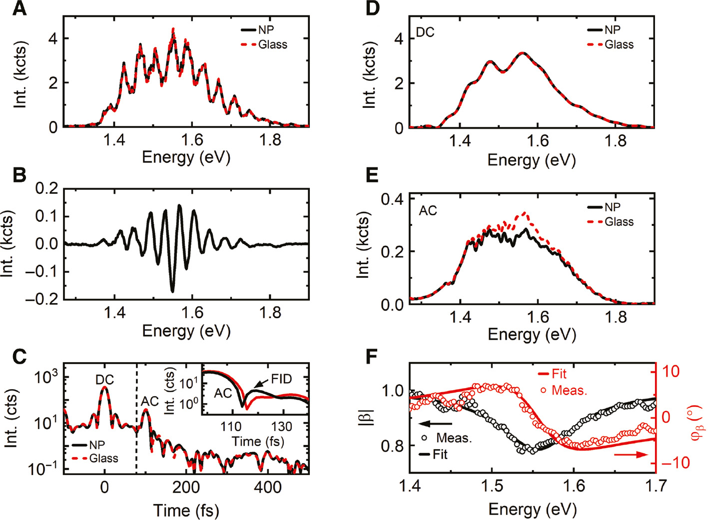
Analysis of PNSI spectra from a single nanorod.
(A) Spectral interferogram recorded from scatterer S3 in Figure 1B, with the tip positioned near the apex of a nanorod (black) or on the glass substrate (red). (B) Difference between the nanorod spectrum and the reference spectrum. (C) Fourier transforms (FTs) of the interferograms in panel (A), showing the amplitude of s0(t) at 0 fs, and the amplitude of the positively delayed AC component s+(t), at ~100 fs time delay. The free induction decay (FID) of the nanorod, leading to a single-sided broadening of s+(t), is highlighted in the inset. (D, E) Temporal separation of s0(t) and s+(t) and their Fourier back-transform into the frequency domain gives (D) |S0(ω)| and (E) |S+(ω)| on glass (dashed red) and near the nanorod apex (solid black). The ratio between S+(ω) on the nanoparticle and on glass provides the absorption by the longitudinal LSP resonance of the particle. (F) Nanorod scattering spectra retrieved (see Section 5) from the AC and DC components in (D, E) and fitted to a Lorentzian line shape model.
![Figure 3: Spatial parameter maps of PNSI spectra of an ensemble of gold nanoparticles.(A) Topography image of the sample showing rod- and sphere-shaped nanoparticles of different sizes. The color scale is leveled off at a height of 13 nm. Capital letters mark the positions of the reconstructed spectra shown in (C), where the experimental data are shown as open circles and fits of the LSP resonance of the nanoparticles to a Lorentzian oscillator model as solid lines. (B, D, E) Parameter maps of the normalized amplitude (B), resonance energy (D), and linewidth (E) of the LSP resonance extracted from the PNSI spectra. At each 5 nm×5 nm pixel of the scan, a full PNSI is recorded and fitted to a Lorentzian oscillator model. Parameters are given only at positions with sufficient nanoparticle near-field amplitude. An increase in scattering amplitude at the apices of the rod-like particles is the signature of the excitation of the longitudinal LSP mode. An increase in line width γ and a red shift of the resonance energy of the LSP resonance near the rod apices result from multiple scattering of near-field photons between the tip and the sample. The resonance energy of spherical particles [dashed circles in (A)] is blue-shifted out of the detection range.](/document/doi/10.1515/nanoph-2019-0397/asset/graphic/j_nanoph-2019-0397_fig_003.jpg)
Spatial parameter maps of PNSI spectra of an ensemble of gold nanoparticles.
(A) Topography image of the sample showing rod- and sphere-shaped nanoparticles of different sizes. The color scale is leveled off at a height of 13 nm. Capital letters mark the positions of the reconstructed spectra shown in (C), where the experimental data are shown as open circles and fits of the LSP resonance of the nanoparticles to a Lorentzian oscillator model as solid lines. (B, D, E) Parameter maps of the normalized amplitude (B), resonance energy (D), and linewidth (E) of the LSP resonance extracted from the PNSI spectra. At each 5 nm×5 nm pixel of the scan, a full PNSI is recorded and fitted to a Lorentzian oscillator model. Parameters are given only at positions with sufficient nanoparticle near-field amplitude. An increase in scattering amplitude at the apices of the rod-like particles is the signature of the excitation of the longitudinal LSP mode. An increase in line width γ and a red shift of the resonance energy of the LSP resonance near the rod apices result from multiple scattering of near-field photons between the tip and the sample. The resonance energy of spherical particles [dashed circles in (A)] is blue-shifted out of the detection range.
Each SI thus shows three peaks [56], [57]: a DC component s0(t), visible at t=0, and two time-delayed AC components at the time delays ±τ0≈±100 fs. The DC component contains the Fourier transform (FT) of the sum of the intensities of the incident and reflected fields, S0(ω)=I0(ω) (1+|σ(ω)|2), with I0(ω)=|Es1(ω)|2 essentially being the laser spectrum modulated by the transmission properties of the grating coupler and the nanotaper [41], [59]. As such, its temporal width is given by the bandwidth-limited pulse duration of the incident and reflected spectra of approximately 7 fs. We isolate s0(t) from the two side peaks along the vertical line in Figure 2C. This temporal separation of DC and AC peaks critically relies on a sufficiently large time delay τ0 and, thus, on a finite distance between the scatterer and the apex. The back-transform of s0 into the spectral domain provides the spectrum of the SPP field at the position of the scatterer (Figure 2D). The DC spectra measured on the nanoparticle position and glass substrate are almost identical, because the intensity of Er is too low to significantly affect this spectrum. The quantities of interest are the side peaks s+/−(t∓τ0). They carry identical information about the cross-correlation between the incident and reflected fields. The back-transform of s+(t−τ0) gives S+(ω)=I0(ω)σ(ω). I0 and σ can be retrieved from S0 and S+ by solving Eq. (3) in Section 5.
In the reference measurement taken on the glass substrate, σR(ω) accounts for the effect of the SPP propagation from the scatterer to the apex and back and for the direct reflection of the SPP waves at the apex. These processes are only weakly wavelength-dependent, and the spectral chirp acquired upon propagation does not significantly affect the time structure of a plasmonic wavepacket [59]. Therefore, the temporal width of s+ is again given by the bandwidth-limited pulse duration of the incident spectrum, and the spectrum |S+(ω)| (red dashed line in Figure 2E) is reasonably similar to the incident spectrum. In the vicinity of the nanorod, the re-emitted field Er enhances the z-component of the field at the apex and thus the reflection coefficient σ(ω)=β(ω)σR(ω) by a frequency-dependent enhancement factor β(ω), which arises from the near-field coupling between the tip and the nanorod (see Section 5). Consequently, the AC cross-terms in Figure 2C show marked differences, since σ(ω) is amplified through heterodyning with I0(ω). In comparison to the reference measurement, s+(t−τ0) thus contains an additional faint contribution with a time structure given by the convolution between the incident field at the apex and the free induction decay (FID) of the nanorod (inset in Figure 2C). For the LSP resonance of our nanorods, this FID decays exponentially with the dephasing time T2=1/γ of about 10–16 fs and thus persists beyond the bandwidth-limited time resolution of our experiment. The backpropagating SPP field induced by the FID is phase-shifted by π with respect to the incident field. Thus, s+(ω) shows a distinct reduction in amplitude around the LSP resonance due to the absorption of light by the nanorod (Figure 2D). On resonance, the amplitude of the backreflected field is reduced by 20%. This implies that about 35% of the nanofocused light at the apex is absorbed by the particle, since for such small rods radiative damping is weak and the scattering cross-section is at least an order of magnitude smaller than the absorption cross-sections [60], [61]. This clearly evidences the efficient localization of the incident light at the apex and the virtually background-free nature of our experiment.
In the final step of our analysis, we extract the coupling-induced enhancement
For the tip-nanorod system investigated here, we consistently find purely absorptive line shapes for all tip-sample configurations and coupling strengths. The reason for observing absorptive line shapes is readily understood. The incident field E0(ω, rt) couples only to the longitudinal component of the tip polarizability
It is important that these PNSI spectra could also be affected by multiple scatterings between different protrusions on the taper shaft. Such multiple scatterings would give rise to new fringe patterns in the PNSI spectra with a modulation frequency given by the scatterer distance. For our tapers, we did not observe such fringe patterns. We therefore conclude that light scattering by these protrusions is so weak that multiple scatterings between the scatterers or between the scatterers and the apex can safely be neglected.
Building upon this quantitative data analysis, we now record two-dimensional maps of PNSI spectra of an ensemble of gold nanoparticles deposited on a glass slide. To this end, we raster-scan the tip apex across the sample surface at a constant tip-sample distance of 2 nm and simultaneously record an SI at each 5 nm×5 nm pixel of the 2D scan within an integration time of 20 ms. These data allow us to spatially map the local light scattering while systematically varying the tip-sample configuration and thus the near-field coupling between the tip and the sample. The sample consists of both rod-like particles (40 nm length, 10 nm diameter) and more spherical nanoparticles, as seen in the topography image, simultaneously recorded by tapping-mode force microscopy, and depicted in Figure 3A. Again, we use a spatially averaged SI recorded with the tip apex placed on the glass substrate for reference to reconstruct spectra β(ω, x, y) at each pixel of the map. These spectra are fitted to Lorentzian line shapes, as discussed for Figure 2. The extracted fitting parameters are then displayed as maps of the local amplitude A(x, y) (panel B), resonance energy ℏω0(x, y) (panel D), and resonance line width ℏγ(x, y) (panel E). We plot these parameters only for those spectra showing a clear absorption resonance. For representative points A–H at the apices of the rod-like nanoparticles, the amplitude and phase of the deduced PNSI spectra β(ω) are shown in Figure 3C. The spectral signature of the coupling to the rod-like nanoparticles is the excitation of the narrow-band longitudinal dipolar LSP resonance at around 1.55 eV with a line width of ~50–80 meV. In addition, the amplitude maps in general show pronounced enhancement in amplitude A when the tip apex is placed close to either of the nanorod apices since the dipolar rod mode interacts with the z-directed tip dipole mainly at the rod apices. The map reflects the intensity profile Iz,LSP(rt)=|Ez,LSP(rt)|2 of the z-component of the fundamental longitudinal LSP mode of the nanorod probed by the tip (see Figure S2, Section 5, and Ref. [26]). When the tip apex is placed exactly over the nanorod center, no excitation of the nanorod is seen since here the z-component of the LSP eigenmode has a node, meaning that at this point the nanorod cannot be optically excited by a vertically oriented point-like source. All these signatures are indeed observed at several positions on the sample, in particular at the positions A–E for which the PNSI spectra are displayed in Figure 3C. The spatial map in Figure 3D reveals very similar resonance energies at the two apices of the same rod (e.g. particles B and D/E) but exhibits a certain variation in the resonance energy of up to 50 meV when moving the tip across each apex of a single nanorod. Concomitantly, the map of the resonance line widths ℏγ(x, y) in Figure 3E shows that close to the nanorod apices a substantial broadening of the observed Lorentzian spectra takes place. We observe line widths of up to 80 meV, i.e. a factor of two broader than determined for the bare nanorod sample investigated by far-field spectroscopy (see Section 5) [26], [60]. Both the spectral red shift and the line broadening imply that for the tip close to a nanorod apex, we are observing multiple scatterings of near-field photons between the tip and the sample. The maps in Figure 3 reveal additional interesting features. Nanoparticles with more spherical shape, such as the two particles marked by white circles in Figure 3A, hardly show up in the PNSI amplitude maps since their LSP resonance is blue-shifted, out of the spectral range of our measurements. A cluster of several nanorods (F–H) shows a response that is distinctly red-shifted with respect to the nanorod LSP. Here, the near-field coupling between several nanorods apparently results in a delocalization of the LSP mode [62] and, thus, a red shift of the SP response, while the line width is only weakly affected by the inter-rod coupling.
To study the tip-sample near-field coupling in more detail, we focus on the PNSI spectra of a single nanorod (marked with points D and E in Figure 3A). High-resolution maps of the topography together with fitted Lorentzian resonance parameters, recorded with a pixel size of 5 nm×5 nm, are displayed in Figure 4A–D. The cross-sections in Figure 4E, extracted along the lines ab and cd in Figure 4A, show that all PNSI spectra (open circles) agree well with a Lorentzian line shape model (red lines), allowing us to faithfully extract the resonance parameters, providing detailed information about the tip-sample coupling. The results in Figure 4B again show a pronounced enhancement of the scattering amplitude A at the two apices of the nanorod, reflecting strong tip-sample coupling. The maps of the line width correlate well with the shape of the amplitude maps (Figure 4D) and reveal an increase in line width by up to 30 meV in the regions of large absorption. In contrast, it appears that the spectral red shift of the LSP resonance is more confined to the rim of the particle, leading to a fundamentally different crescent-moon shape [26].
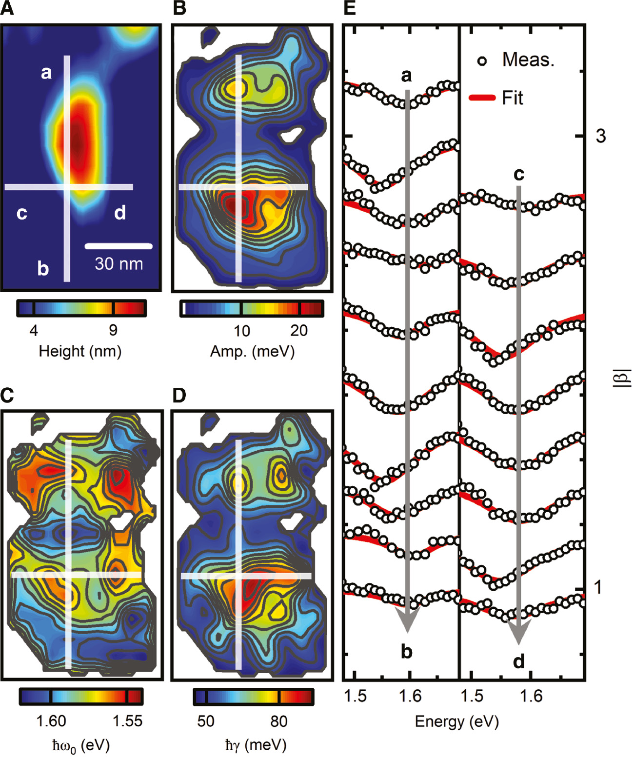
Line-shape analysis of PNSI spectra near a single gold nanorod.
(A) AFM topography image of the nanorod. (B–D) Parameter maps of the normalized amplitude (B), resonance energy (C), and line width (D) of the LSP resonance extracted from the PNSI spectra. At each pixel of the scan, a PNSI spectrum is reconstructed from a referenced SI and fitted to a Lorentzian line shape. The maps of the resonance amplitude (B) and the line width (D) show the two-lobed intensity profile of the longitudinal nanorod LSP mode, while the resonance energy (C) shows a more complicated pattern with enhanced red shifts near the rim of the nanorod. (E) PNSI spectra (open circles) taken along the lines a–b and c–d in panel (A), emphasizing the red shift of the LSP resonance near the rim of the nanorod. The solid red lines are fits to a Lorentzian oscillator model.
These findings are readily understood. The normalized amplitude map essentially follows the intensity profile Iz,LSP(rt) of the z-component of the electric field emitted by the fundamental longitudinal LSP mode of the nanorod (Figure S2). The tip acts as a point-like excitation source, inducing a rod polarizability that is proportional to the amplitude of the z-component of the electric field of the LSP eigenmode Ez,LSP(rt) at the position of the tip. It then senses the z-component of the field generated by this polarizability, again following the mode profile, resulting in a secondary tip polarizability that scales with Iz,LSP(rt). This coupling of the nanorod dipole to the longitudinal tip polarization can be considered as an additional loss channel for the nanorod LSP mode since it induces a backpropagating SPP field on the taper and, with smaller probability, an enhanced radiative damping of the LSP mode. This Purcell effect [63], [64] causes the increase in line width near the apices of the rod [26]. The damping rate is proportional to the mode intensity Iz,LSP(rt), and hence the increase in line width is expected to show the same spatial dependence as the amplitude map. Within the noise limit of our experiment, this correlation between the amplitude and line width maps is seen reasonably well in Figure 4B and D. The peculiar crescent-moon shape in the resonance energy has also been seen, with somewhat higher spatial resolution, in our recent study of vectorial near-field couplings [26]. The prominent red shift of up to 50 meV at the rims of the nanorods results from the coupling of the LSP resonance of a nanorod to the transversal tip polarizability
To confirm this discussion of our results and to verify our model for the analysis of PNSI spectra, we simulated the time dynamics of the electromagnetic (EM) field along a conical taper interacting with a nanorod. Full-wave numerical finite-difference time-domain (FDTD) simulations of the experiment have been performed using both self-written [65] and commercial (Lumerical) Maxwell solvers. The geometry of the simulation is illustrated in Figure 5A. A conical gold taper with an opening angle of 15° and 10 nm apex radius is placed at a few nanometers away from a gold nanorod of dimensions 60 nm×10 nm×10 nm (see inset) with a longitudinal LSP resonance at 1.55 eV. The computational domain is discretized with nonuniform meshing with step size ~1 nm in the near-field region including the nanorod and the tip apex and a coarser mesh of ~10 nm step size for the rest. The conical structure is terminated at ~2 μm distance from the apex to limit the computational cost. A short 7 fs pulse centered at 1.55 eV excites solely the symmetric m=0 mode of the taper, avoiding the excitation of higher order |m|>0 modes. This SPP pulse propagates along the shaft and is nanofocused to the apex with negligible mode mixing, as depicted in Figure 5B, showing the time evolution of the x-component of the SPP field. It is then coupled to the longitudinal LSP mode of the nanorod, exciting resonant dipole oscillations of the rod (Figure 5B, middle), and partially reflected back to the shaft (Figure 5B, right). The time dynamics of the Ex component of the electric field at point A on the shaft (Figure 5A) shows the incident pulse together with a reflected pulse, while that at point B near the particle resolves the FID of the nanorod. Evidently, the pulse duration of the incident pulse is shorter than the 10-fs dephasing time of the simulated LSP resonance. Comparing the reflected pulse at point A to the FID of the rod at point B, we observe that the former is composed of two beating components: one is directly reflected from the apex without interaction with the nanorod, and the other shows the nanorod dipole oscillations which are coupled back to the tip and propagate backwards. Even for these short 7-fs pulses, the group velocity dispersion of the m=0 mode and the reflection near the apex have essentially no effect on the pulse duration. The second reflection component contains the desired information about the FID of the particle. It vanishes completely when we increase the tip-sample distance from 10 nm (“near” position) to 100 nm (“far” position), moving the rod out of the near field of the tip. The phase shift of π between the directly reflected SPP pulse and the pulse induced by the FID of the rod can be discerned from the time structure of the reflected pulse at point A. The SIs of the field component Ex at point A are shown in Figure 5C for the sample positions close to and far away from the tip. They demonstrate the vanishing of the resonant nanorod absorption at 1.55 eV when moving the rod out of the tip’s near field. A time-domain separation of the reflected field at A from the incident field makes it easier to observe the nanorod signature in the spectra shown in Figure 5D. As we calculate at the field level, this separation can directly be performed in the time domain without the need for the algorithm described for the analysis of the intensity-level experimental data in Figure 2. The FT of the reflected fields results in complex-valued spectra containing both the amplitude and phase of the electric field emitted by the nanorod. The longitudinal LSP resonance of the particle is clearly observed by a comparison of the reflection spectra with and without near-field coupling between the tip and the sample in Figure 5D. Similar to the method used for extracting the phase-resolved scattering spectra from the experimental data in Figure 2E, a normalization of the complex-valued spectrum recorded with the tip close to the nanorod to that at 100-nm distance leads to an absorptive PNSI spectrum with Lorentzian line shape in Figure 5E. Amplitude, resonance energy, and line width of the simulated PNSI spectrum agree reasonably well with those deduced in Figure 2. We consider this convincing support for our experimental technique.
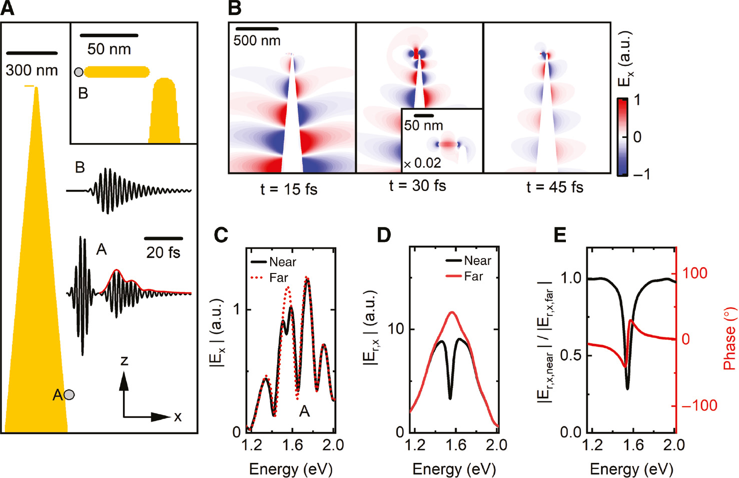
Finite-difference time-domain simulation of the PNSI experiment.
(A) A conical gold tip is excited by a 7-fs SPP pulse in the m=0 mode. The nanofocused SPP pulse couples to a small gold nanorod (see inset). The field component Ex at point A shows the incident pulse followed by the pulse Er,x backreflected from the apex. Er,x contains the directly reflected apex field and the re-emitted nanorod field. Near the rod apex (point B), the field shows the nanorod FID. (B) Snapshots of Ex demonstrating the nanofocusing of SPPs to the apex (left), their interaction with the rod (middle), and backpropagation (right). The inset highlights the excitation of the nanorod. (C) FT spectrum of Ex at point A for tip-nanorod distances of 3 nm (“near”, black) and 100 nm (“far”, red). The near-field coupling to the rod is seen around 1.55 eV. (D) FT of Er,x at point A, emphasizing light absorption by the nanorod (black). (E) Amplitude (black) and phase spectrum (red) obtained by normalizing the complex-valued FT spectra of Er,x when the tip is “near” the rod to that with the tip “far” from it.
3 Discussion
The PNSI spectra presented in this work fulfill many of the requirements for a faithful imaging of the projected local optical density of states by near-field spectroscopic techniques. The projected LDOS [5], [66]
probes one component of the electric field E(rt, ω)=μ0ω2
In the limit of sufficiently weak losses, the projected LDOS may be expressed in a mode representation as [5], [34]
Here, en(rt) denotes the electric field profile of the nth appropriately normalized [67], [68], [69] eigenmode of the system. In our proof-of-principle experiments, we essentially probe only a single eigenmode in the covered spectral region, namely the longitudinal LSP resonance of the gold nanorod. A spectrally resolved LDOS measurement therefore provides the resonance energy and line width of this particular mode, while a spatial map gives the intensity profile of a specific field component of the eigenmode. Both requirements are met in our measurements. The map of the PNSI amplitude in Figure 4B indeed provides a spatially highly resolved map of the intensity of the z-component of the LSP field. Resonance energy and line width can be extracted with high fidelity from the PNSI spectra, as illustrated in Figure 2 and supported by the results of the FDTD simulations presented in Figure 5. All these results support the conclusion that PNSI spectroscopy can indeed provide a quantitative measure of the LDOS, projected onto the direction given by the taper axis.
Such a quantitative mapping is, of course, provided only in the limit where multiple near-field scattering between the tip and the sample is weak and does not affect the parameters deduced from the experiment. Evidently, this is not yet the case in the proof-of-principle experiments, since it is clear from the results presented in Figure 4 that the coupling between the tip and the sample induces both an increase in line width (Purcell effect) and a spectral red shift of the rod resonance (optical Stark effect). Clearly, the tip is invasive, and multiple near-field scattering needs to be considered in the data analysis. At first sight, this may be considered a substantial drawback of the presented technique, in particular when comparing it to less invasive techniques such as EELS in which such higher order effects may safely be neglected and first-order perturbation theory is sufficient to quantitatively describe the experimental results. An obvious approach to overcome such tip-sample couplings is to slightly increase the tip-sample distance until line width broadenings and resonance energy shifts vanish. For the sharp tips used in the present experiments, with optical near fields that are closely confined to their apex, it only takes distances of 5–10 nm to largely suppress multiple tip-sample scattering, even for strong near-field scatterers such as the nanorods studied in the present work [26]. This is readily verified by coupled dipole simulations shown in Figure S2. When increasing the tip-sample distance to 5 nm, the amplitude of the PNSI reduces approximately by a factor of four, still giving sufficiently large scattering signals to retrieve the PNSI spectra. Since the coupling-induced line broadening and resonance energy shifts result from multiple scatterings between the tip and the sample, they decay even more quickly with increasing tip-sample distance. For 8-nm distance, the coupled dipole simulations predict weak line broadenings and red shifts of less than 10 meV. At such a distance, the LDOS can be quantitatively retrieved, essentially with negligible coupling-induced resonance changes and with a high spatial resolution of better than 10 nm. Since in the present work both the tip and the nanorod are strong near-field scatterers, even shorter distances are sufficient to suppress such tip-sample couplings in other experiments. The recording of spectra at variable distances can thus help ensure that multiple scattering effects are indeed sufficiently weak to not affect the optical response [26]. Alternatively, a modification of the apex region, for example by attaching a small dielectric scatterer, could allow control and suppression of multiple near-field scattering.
We are convinced, however, that the results presented in this work suggest that it is more appropriate to think in a different direction and to consider this sensitivity to multiple near-field scattering a particular strength of the presented method, rather than a weakness. The results of the FDTD simulations shown in Figure 5 are a promising step towards a quantitative understanding of these tip-sample interactions and indicate that they represent a unique means to not just sense but also to manipulate and control optics at the nanoscale. Such an improved understanding of near-field couplings forms a solid foundation for using PNSI for quantitative LDOS mapping.
4 Summary and conclusions
In summary, we have presented a new experimental technique, namely PNSI, to sense the amplitude and phase of the electric field emitted by a single nanostructure over a wide spectral range. The key to this method is the use of the single-mode waveguiding characteristics of a conical gold taper with a sharply pointed tip. Plasmonic nanofocusing creates a bright and spatially isolated nano-light source at its apex with well-controlled polarization properties. The taper is used not only to locally excite the sample but also to scatter optical near fields into SPP waves that are backpropagating along the taper shaft. We read out these backward propagating SPP waves and their interference with incident SPP waves by scattering them off the taper. The recorded interferograms provide a local light scattering spectrum of the sample. By probing the longitudinal LSP resonance of a small gold nanorod, we showed, both experimentally and theoretically, that the recorded PNSI spectra quantitatively map the projected local optical density of states of the sample in the limit of sufficiently weak tip-sample interactions. This is evidenced, in particular, by observing purely absorptive PNSI spectra, as opposed to more complex Fano-type line shapes seen in spectra that directly collect the light scattered from the taper apex. In addition, we showed that the amplitude of the PNSI maps the intensity profile of the field component of the nanorod mode that is polarized along the taper axis, a second important signature of projected LDOS imaging. The broad spectrum supported by the conical gold taper and the efficient conversion of optical near fields into SPPs at the sharp apex of the taper are the key to sensitive LDOS mapping with a spatial resolution of better than 10 nm.
The recorded PNSI spectra probe near-field couplings between the tip and the sample with high sensitivity and show how multiple scatterings between the nanorod and the anisotropic tip scatterer result in local line broadenings and resonance energy shifts of the probed nanorod resonance. For small tip-sample distances, the coupling of the rod’s near field to taper SPPs enhances the damping of the nanorod resonance, and this results in line broadenings when placing the tip close to the nanorod ends. In contrast, optical Stark shifts of the nanorod resonance due to its coupling to the transverse polarizability component of the taper show up within a distinctly different spatial signature near the rims of the nanorod. While these multiple near-field couplings can easily be suppressed by increasing the tip-sample distance or by changing the apex composition, the ability to probe these couplings with high sensitivity is a promising new aspect of our results. We anticipate that this sensitivity may be particularly beneficial for reading out and controlling quantum emitters and their coupling to radiative environments [70], [71], a fundamental challenge in nano-optics. PNSI thus represents a new and particularly sensitive approach towards this goal, not only because it can sense linear light scattering with high spatial resolution and in a broad spectral range but also because broadband and essentially chirp-free response of the employed conical tapers makes the technique particularly well suited for time-resolved studies and for bringing multidimensional optical spectroscopies to the nanoscale. Earlier measurements have already shown that plasmonic nanofocusing can result in few-cycle nanofocused light or electron sources when coupling few-cycle light pulses to the grating coupler [39], [59], [72], [73]. This makes ultrafast PNSI a highly promising new tool for probing the dynamics of optical excitations at the nanoscale.
5 Methods
5.1 Experiments
5.1.1 Sample preparation
Nanoparticle samples were prepared and characterized following the method described in Ref. [26]. Chemically synthesized, polymer-coated gold nanorods (NanoPartz Inc., Loveland, CO, USA, Part. No. A12-10-808) were deposited on BK7 glass substrates (pretreated with Piranha solution and hydroxylated through UV/O3 exposure) by immersing the substrates in a dried ethanol suspension of particles (specified concentration of 2.9×10⁹ ml−1) for 24 h. After retrieval, the samples were rinsed in deionized water and blow-dried under an argon stream. The nanorods were then optically characterized by FT spectroscopy [60]. Extinction spectra of 39 individual particles showed a longitudinal surface plasmon resonance energy of 1.6±0.1 eV, an associated extinction cross-section of 3500±900 nm2, and a line width ℏγ≃0.04 eV.
5.1.2 Nanotaper preparation
Nanofocusing gold tapers were produced using the wet chemical etching method described in Refs. [26], [59]. Gold wires of 125 μm diameter (Advent Research Materials) were annealed at 800°C for 8 h and electrochemically etched in concentrated hydrochloric acid (37%) using a platinum ring as the counter electrode. The etched tapers were rinsed in ethanol and inspected under a scanning electron microscope (SEM, FEI, Helios Nanolab 600i). We found that some tapers exhibited individual colloidal precipitates of typically 100 nm diameter on the shaft (Figure 1A, right inset). These are most likely small gold precipitates that are formed naturally during etching. Their density is typically very low and we find at most a few of them in the relevant region of the taper. Hence, they serve as spatially isolated local scatterers, converting a small fraction of the SPP field on the tip shaft into far-field radiation, allowing for the observation of pronounced spectral interferograms as shown in Figure 1C.
Three-line grating couplers (1.26 μm period, 100 nm width, 200 nm depth) were produced by focused Ga+-ion beam lithography 50 μm above the taper apex of 10 nm radius. The grating lines were slightly inclined with respect to each other to increase the optical coupling bandwidth, resulting in a 200-nm change in grating period across the taper [74].
5.1.3 Plasmonic nanofocusing spectral interferometry experiments
For launching SPPs, a broadband supercontinuum laser (Fianium WL-SC-400-4 650 nm – 900 nm spectral bandwidth) was focused onto the grating coupler. We used a microscope objective with a numerical aperture of NA=0.2, which was inclined by 13° out of the sample plane, thus avoiding any direct illumination of the sample or the tip apex. A half-wave plate was used to adjust the polarization state of the light impinging on the grating coupler to p-polarization for highest SPP coupling efficiency. The scattered optical signals were detected by a separate collection objective at an angle of ~20° out of the sample plane with a numerical aperture of NA=0.35. Using an iris placed in an intermediate image plane, which was simultaneously monitored on an auxiliary camera (marked CCD in Figure 1A), we could separately collect the scattered light from either the taper apex or any of the three individual scatterers along the shaft (Figure 1B). After spatial filtering, the scattered light was spectrally dispersed using a monochromator (Princeton Instruments, Acton SP2500) and spectra were recorded with a liquid-nitrogen-cooled charge-coupled device (CCD) camera (Roper Scientific, Spec-10:100BR).
Tip-sample distance regulation was realized with a custom-built tuning-fork-based AFM similar to the setup described in Refs. [49], [54]. The nanofocusing SNOM taper was glued to one prong of a quartz tuning fork which was electrically driven in resonance to oscillate normal to the sample surface with a peak-to-peak amplitude of ~1 nm. By PID feedback control, one axis of a 3D piezo-actuator (PI, P-363.3CD) kept the tip-sample distance at ~2 nm. The other two axes of the 3D piezo-actuator were used to laterally raster-scan the sample surface.
5.2 Theoretical modeling
In the first part of this section, we formalize the process of signal formation in PNSI based on the simplest conceivable modeling approach, presenting the tip and the sample as coupled electromagnetic point dipoles with Lorentzian spectral responses. Using this model, we show that the measured SIs contain full information about the local scattering spectrum of the investigated gold nanorods and allow the reconstruction of the local density of plasmonic states around the nanorods projected along the nanofocusing tip axis. In the second part, we describe the experimental data analysis and show how both local scattering spectra and projected LDOS are extracted from the measured SIs. The model developed here is an extension of that described in Refs. [26], [49]. Based on this coupled dipole model, we have performed additional simulations of the maps in Figure 4, which are in convincing agreement with the experiments (see Supporting Information).
5.2.1 Coupled dipole model for plasmonic nanofocusing spectral interferometry
We follow the approach introduced in Ref. [26] to account for near-field coupling between the tip and the sample. We approximate the nanotaper apex and the gold nanorod as dipolar point scatterers, which interact via both their optical near and far fields. We capture the optical response of the tip apex by a point-like diagonal polarizability tensor
Experimentally, the tip apex is excited both by the spectrally broadband external SPP field E0(ω, rt) nanofocused at the tip apex at position rt and any secondary fields Er(ω, rt) that are emitted by the nanorod. The resulting apex field Ea=E0+Er induces a dipole moment
We then expand the multiple scattering interaction between the tip and the sample in a perturbation series. We assume that the nanorod is only excited through the near and far fields emitted by the tip apex upon initial excitation. In first order, the local rod dipole moment induced by the zero-order tip field
Here, the Green’s function
Within this model, higher order contributions to the field emitted by the nanorod are given as
Here, we introduce a coupling-induced field enhancement factor β(ω)=((I−M)−1)zz. This PNSI spectrum describes the effect of the near-field coupling between the tip and the sample on the z-component of the local field at the apex and, thus, on the amplitude of the backpropagating SPP field. In first order, β(ω) reduces to β(1)(ω)=1+Mzz(ω, rt) and thus contains the desired information about the LDOS of the nanorod. The higher order field components
5.2.2 Data analysis in plasmonic nanofocusing spectral interferometry
We now discuss how we extract the information about the electric fields emitted by the nanorod and the projected LDOS ρe,z(ω, rt) from the experimentally measured SIs. As illustrated in Figure 1A, we focus a broadband laser field EL(ω) on the grating coupler to launch SPP waves at the taper shaft. The resulting SPP field Es1(ω, rs) that is reaching the scatterer at position rs is a coherent superposition of several radially polarized SPP eigenmodes of the cylindrical taper and can be expressed as
The role of the point-like protrusion on the shaft is to scatter both Es1 and Es2 and to create the fields
The measured SI then expands as
If the time delay τ0 is larger than the temporal width of each peak, the three components can be isolated, as illustrated in Figure 2C. Fourier back-transformation of the zero-delay component gives S0(ω)=I0(ω)(1+|σ(ω)|2), containing mainly information about the amplitude of the incident spectrum I0(ω) as |σ(ω)|2<1. Both the negatively delayed component S−(ω)=I0(ω)σ*(ω) and the positively delayed component S+(ω)=I0(ω)σ(ω) are complex-valued and contain identical information of the amplitude |σ(ω)| and phase φσ(ω) of
Since I0(ω) is a real number, we can directly obtain the phase of the reflection coefficient as
It is evident that a single measurement does not yet allow us to deduce the desired coupling-induced field enhancement β(ω) but gives
5.2.3 Finite-difference time-domain simulations
We first used an in-house-developed simulation toolbox in MATLAB language [65] for simulating linear [48] and nonlinear [65] optical systems as well as EELS [29] and CL [78] spectra. We calculated the field profile and the propagation constant of the m=0 mode of a gold fiber and used this profile to excite the gold taper. Initial simulations were performed with a discretization unit of 25 nm, showing the propagation and the reflection of SPPs and the FID of the nanorod sample. Higher resolution simulations, performed using Lumerical to allow for multiple-gridding, are shown in Figure 5.
6 Supporting information
The following files are available free of charge. Simulation of the spectral interferometry algorithm. Coupled dipole simulation of the near-field interaction (Esmann_SI_SOM_F.pdf).
Acknowledgments
Financial support by the Deutsche Forschungsgemeinschaft (SPP1839 “Tailored Disorder”, LI 580/12, SPP1840, GRK 1885, Funder Id: http://dx.doi.org/10.13039/501100001659, SFB 1372) and the German-Israeli Foundation (GIF grant no. 1256) is gratefully acknowledged. JZ acknowledges support by a Carl von Ossietzky Fellowship of the University of Oldenburg and from the Alexander von Humboldt Foundation. AC is supported by German Academic Exchange Service (DAAD) through a Ph.D. scholarship. AK acknowledges the financial support from the Graduate Program “Nanoenergy Research” of the State of Lower Saxony. ME thanks the Studienstiftung des Deutschen Volkes (German Scholarship Foundation) for a Ph.D. scholarship and the Deutsche Forschungsgemeinschaft (project 401390650). NT acknowledges funding from the European Research Council, ERC-Starting Grant NanoBeam. The simulations were performed at the HPC Cluster CARL funded through DFG INST 184/157-1 FUGG, INST 184/158-1 FUGG, Funder Id: http://dx.doi.org/10.13039/501100001659 and the Ministry of Science and Culture (MWK) of the Lower Saxony State.
Author contributions: The manuscript was written through contributions of all authors. All authors have given approval to the final version of the manuscript. ME and CL initiated the research. JW and GW prepared the nanorod samples. ME performed the measurements. ME and AC analyzed the data and prepared the figures with help of AK and JHZ. AC and SS performed the FDTD simulations. AC, ME, and CL co-wrote the manuscript with contributions from all authors. GW and CL supervised the project.
References
[1] Crommie MF, Lutz CP, Eigler DM. Confinement of electrons to quantum corrals on a metal-surface. Science 1993;262:218–20.10.1126/science.262.5131.218Suche in Google Scholar PubMed
[2] Crommie MF, Lutz CP, Eigler DM. Imaging standing waves in a 2-dimensional electron-gas. Nature 1993;363:524–7.10.1038/363524a0Suche in Google Scholar
[3] Manoharan HC, Lutz CP, Eigler DM. Quantum mirages formed by coherent projection of electronic structure. Nature 2000;403:512–5.10.1038/35000508Suche in Google Scholar PubMed
[4] Fiete GA, Heller EJ. Colloquium: theory of quantum corrals and quantum mirages. Rev Mod Phys 2003;75:933–48.10.1103/RevModPhys.75.933Suche in Google Scholar
[5] Carminati R, Caze A, Cao D, et al. Electromagnetic density of states in complex plasmonic systems. Surf Sci Rep 2015;70:1–41.10.1016/j.surfrep.2014.11.001Suche in Google Scholar
[6] Joulain K, Carminati R, Mulet J-P, Greffet J-J. Definition and measurement of the local density of electromagnetic states close to an interface. Phys Rev B 2003;68:245405.10.1364/IQEC.2004.IWA29Suche in Google Scholar
[7] Yablonovitch E. Inhibited spontaneous emission in solid-state physics and electronics. Phys Rev Lett 1987;58:2059–62.10.1007/978-1-4615-1963-8_41Suche in Google Scholar
[8] Chicanne C, David T, Quidant R, et al. Imaging the local density of states of optical corrals. Phys Rev Lett 2002;88:097402.10.1103/PhysRevLett.88.097402Suche in Google Scholar PubMed
[9] Dereux A, Girard C, Chicanne C, et al. Subwavelength mapping of surface photonic states. Nanotechnology 2003;14:935–8.10.1088/0957-4484/14/8/317Suche in Google Scholar
[10] Wang Q, Stobbe S, Lodahl P. Mapping the local density of optical states of a photonic crystal with single quantum dots. Phys Rev Lett 2011;107:167404.10.1103/PhysRevLett.107.167404Suche in Google Scholar PubMed
[11] Krachmalnicoff V, Cao D, Cazé A, et al. Towards a full characterization of a plasmonic nanostructure with a fluorescent near-field probe. Opt Express 2013;21:11536–45.10.1364/OE.21.011536Suche in Google Scholar PubMed
[12] Koenderink AF, Bechger L, Schriemer HP, Lagendijk A, Vos WL. Broadband fivefold reduction of vacuum fluctuations probed by dyes in photonic crystals. Phys Rev Lett 2002;88:143903.10.1103/PhysRevLett.88.143903Suche in Google Scholar PubMed
[13] Farahani JN, Pohl DW, Eisler HJ, Hecht B. Single quantum dot coupled to a scanning optical antenna: a tunable superemitter. Phys Rev Lett 2005;95:017402.10.1103/PhysRevLett.95.017402Suche in Google Scholar PubMed
[14] Huang C, Bouhelier A, Francs GC, Legay G, Weeber JC, Dereux A. Far-field imaging of the electromagnetic local density of optical states. Opt Lett 2008;33:300–2.10.1364/OL.33.000300Suche in Google Scholar
[15] De Wilde Y, Formanek F, Carminati R, et al. Thermal radiation scanning tunnelling microscopy. Nature 2006;444:740–3.10.1038/nature05265Suche in Google Scholar PubMed
[16] Girard C, David T, Chicanne C, et al. Imaging surface photonic states with a circularly polarized tip. Europhys Lett 2004;68:797–803.10.1209/epl/i2004-10290-6Suche in Google Scholar
[17] Esslinger M, Vogelgesang R. Reciprocity theory of apertureless scanning near-field optical microscopy with point-dipole probes. ACS Nano 2012;6:8173–82.10.1021/nn302864dSuche in Google Scholar PubMed
[18] Neuman T, Alonso-Gonzalez P, Garcia-Etxarri A, Schnell M, Hillenbrand R, Aizpurua J. Mapping the near fields of plasmonic nanoantennas by scattering-type scanning near-field optical microscopy. Laser Photon Rev 2015;9:637–49.10.1002/lpor.201500031Suche in Google Scholar
[19] Burresi M, Engelen RJP, Opheij A, et al. Observation of polarization singularities at the nanoscale. Phys Rev Lett 2009;102:033902.10.1103/PhysRevLett.102.033902Suche in Google Scholar PubMed
[20] Lee KG, Kihm HW, Kihm JE, et al. Vector field microscopic imaging of light. Nat Photon 2007;1:53–6.10.1038/nphoton.2006.37Suche in Google Scholar
[21] Schnell M, Garcia-Etxarri A, Alkorta J, Aizpurua J, Hillenbrand R. Phase-resolved mapping of the near-field vector and polarization state in nanoscale antenna gaps. Nano Lett 2010;10: 3524–8.10.1021/nl101693aSuche in Google Scholar
[22] Olmon RL, Rang M, Krenz PM, et al. Determination of electric-field, magnetic-field, and electric-current distributions of infrared optical antennas: a near-field optical vector network analyzer. Phys Rev Lett 2010;105:167403.10.1103/PhysRevLett.105.167403Suche in Google Scholar
[23] Knoll B, Keilmann F. Enhanced dielectric contrast in scattering-type scanning near-field optical microscopy. Opt Commun 2000;182:321–8.10.1016/S0030-4018(00)00826-9Suche in Google Scholar
[24] Raschke MB, Lienau C. Apertureless near-field optical microscopy: tip-sample coupling in elastic light scattering. Appl Phys Lett 2003;83:5089–91.10.1063/1.1632023Suche in Google Scholar
[25] Garcia-Etxarri A, Romero I, de Abajo FJG, Hillenbrand R, Aizpurua J. Influence of the tip in near-field imaging of nanoparticle plasmonic modes: weak and strong coupling regimes. Phys Rev B 2009;79:125439.10.1103/PhysRevB.79.125439Suche in Google Scholar
[26] Esmann M, Becker SF, Witt J, et al. Vectorial near-field coupling. Nat Nanotechnol 2019;14:698–704.10.1038/s41565-019-0441-ySuche in Google Scholar PubMed
[27] Losquin A, Camelio S, Rossouw D, et al. Experimental evidence of nanometer-scale confinement of plasmonic eigenmodes responsible for hot spots in random metallic films. Phys Rev B 2013;88:115427.10.1103/PhysRevB.88.115427Suche in Google Scholar
[28] Ogut B, Talebi N, Vogelgesang R, Sigle W, van Aken PA. Toroidal plasmonic eigenmodes in oligomer nanocavities for the visible. Nano Lett 2012;12:5239–44.10.1021/nl302418nSuche in Google Scholar PubMed
[29] Talebi N, Sigle W, Vogelgesang R, et al. Excitation of mesoscopic plasmonic tapers by relativistic electrons: phase matching versus eigenmode resonances. ACS Nano 2015;9:7641–8.10.1021/acsnano.5b03024Suche in Google Scholar PubMed
[30] Nelayah J, Kociak M, Stephan O, et al. Mapping surface plasmons on a single metallic nanoparticle. Nat Phys 2007;3: 348–53.10.1038/nphys575Suche in Google Scholar
[31] García de Abajo FJ, Kociak M. Probing the photonic local density of states with electron energy loss spectroscopy. Phys Rev Lett 2008;100:106804.10.1103/PhysRevLett.100.106804Suche in Google Scholar PubMed
[32] García de Abajo FJ. Optical excitations in electron microscopy. Rev Mod Phys 2010;82:209–75.10.1103/RevModPhys.82.209Suche in Google Scholar
[33] Hohenester U, Ditlbacher H, Krenn JR. Electron-energy-loss spectra of plasmonic nanoparticles. Phys Rev Lett 2009;103:106801.10.1103/PhysRevLett.103.106801Suche in Google Scholar PubMed
[34] Losquin A, Kociak M. Link between cathodoluminescence and electron energy loss spectroscopy and the radiative and full electromagnetic local density of states. ACS Photon 2015;2:1619–27.10.1021/acsphotonics.5b00416Suche in Google Scholar
[35] Kuttge M, Vesseur EJR, Koenderink AF, et al. Local density of states, spectrum, and far-field interference of surface plasmon polaritons probed by cathodoluminescence. Phys Rev B 2009;79:113405.10.1103/PhysRevB.79.113405Suche in Google Scholar
[36] Talebi N. Interaction of electron beams with optical nanostructures and metamaterials: from coherent photon sources towards shaping the wave function. J Opt 2017;19:103001.10.1088/2040-8986/aa8041Suche in Google Scholar
[37] Krivanek OL, Lovejoy TC, Dellby N, et al. Vibrational spectroscopy in the electron microscope. Nature 2014;514:209–12.10.1002/9783527808465.EMC2016.6064Suche in Google Scholar
[38] Lourenco-Martins H, Kociak M. Vibrational surface electron-energy-loss spectroscopy probes confined surface-phonon modes. Phys Rev X 2017;7:041059.10.1103/PhysRevX.7.041059Suche in Google Scholar
[39] Jiang T, Kravtsov V, Tokman M, Belyanin A, Raschke MB. Ultrafast coherent nonlinear nanooptics and nanoimaging of graphene. Nat Nanotechnol 2019;14:838–43.10.1038/s41565-019-0515-xSuche in Google Scholar PubMed
[40] Stockman MI. Nanofocusing of optical energy in tapered plasmonic waveguides. Phys Rev Lett 2004;93:137404.10.1103/PhysRevLett.93.137404Suche in Google Scholar PubMed
[41] Ropers C, Neacsu CC, Elsaesser T, Albrecht M, Raschke MB, Lienau C. Grating-coupling of surface plasmons onto metallic tips: a nanoconfined light source. Nano Lett 2007;7:2784–8.10.1021/nl071340mSuche in Google Scholar PubMed
[42] De Angelis F, Das G, Candeloro P, et al. Nanoscale chemical mapping using three-dimensional adiabatic compression of surface plasmon polaritons. Nat Nanotechnol 2009;5:67–72.10.1038/nnano.2009.348Suche in Google Scholar PubMed
[43] Sadiq D, Shirdel J, Lee JS, Selishcheva E, Park N, Lienau C. Adiabatic nanofocusing scattering-type optical nanoscopy of individual gold nanoparticles. Nano Lett 2011;11:1609–13.10.1021/nl1045457Suche in Google Scholar PubMed
[44] Neacsu CC, Berweger S, Olmon RL, Saraf LV, Ropers C, Raschke MB. Near-field localization in plasmonic superfocusing: a nanoemitter on a tip. Nano Lett 2010;10:592–6.10.1021/nl903574aSuche in Google Scholar PubMed
[45] Berweger S, Atkin JM, Olmon RL, Raschke MB. Adiabatic tip-plasmon focusing for nano-Raman spectroscopy. J Phys Chem Lett 2010;1:3427–32.10.1021/jz101289zSuche in Google Scholar
[46] Berweger S, Atkin JM, Olmon RL, Raschke MB. Light on the tip of a needle: plasmonic nanofocusing for spectroscopy on the nanoscale. J Phys Chem Lett 2012;3:945–52.10.1021/jz2016268Suche in Google Scholar PubMed
[47] Giugni A, Allione M, Torre B, et al. Adiabatic nanofocusing: spectroscopy, transport and imaging investigation of the nano world. J Opt 2014;16:114003.10.1088/2040-8978/16/11/114003Suche in Google Scholar
[48] Gross P, Esmann M, Becker SF, Vogelsang J, Talebi N, Lienau C. Plasmonic nanofocusing – grey holes for light. Adv Phys X 2016;1:297–330.10.1080/23746149.2016.1177469Suche in Google Scholar
[49] Becker SF, Esmann M, Yoo K, et al. Gap-plasmon-enhanced nanofocusing near-field microscopy. ACS Photon 2016;3: 223–32.10.1021/acsphotonics.5b00438Suche in Google Scholar
[50] Jiang R-H, Chen C, Lin D-Z, Chou H-C, Chu J-Y, Yen T-J. Near-field plasmonic probe with super resolution and high throughput and signal-to-noise ratio. Nano Lett 2018;18:881–5.10.1021/acs.nanolett.7b04142Suche in Google Scholar PubMed
[51] Kim S, Yu N, Ma X, et al. High external-efficiency nanofocusing for lens-free near-field optical nanoscopy. Nat Photon 2019;13:636–43.10.1038/s41566-019-0456-9Suche in Google Scholar
[52] Liu S, Müller M, Sun Y, et al. Resolving the correlation between tip-enhanced resonance raman scattering and local electronic states with 1 nm resolution. Nano Lett 2019;19:5725–31.10.1021/acs.nanolett.9b02345Suche in Google Scholar PubMed PubMed Central
[53] Pfeiffer CA, Economou EN, Ngai KL. Surface polaritons in a circularly cylindrical interface – surface plasmons. Phys Rev B 1974;10:3038–51.10.1103/PhysRevB.10.3038Suche in Google Scholar
[54] Esmann M, Becker SF, da Cunha BB, et al. k-Space imaging of the eigenmodes of sharp gold tapers for scanning near-field optical microscopy. Beilstein J Nanotechnol 2013;4:603–10.10.3762/bjnano.4.67Suche in Google Scholar PubMed PubMed Central
[55] Reynaud F, Salin F, Barthelemy A. Measurement of phase-shifts introduced by nonlinear optical phenomena on subpicosecond pulses. Opt Lett 1989;14:275–7.10.1364/OL.14.000275Suche in Google Scholar
[56] Lepetit L, Cheriaux G, Joffre M. Linear techniques of phase measurement by femtosecond spectral interferometry for applications in spectroscopy. J Opt Soc Am B 1995;12:2467–74.10.1364/JOSAB.12.002467Suche in Google Scholar
[57] Dorrer C, Belabas N, Likforman JP, Joffre M. Spectral resolution and sampling issues in Fourier-transform spectral interferometry. J Opt Soc Am B 2000;17:1795–802.10.1364/JOSAB.17.001795Suche in Google Scholar
[58] Yi JM, Hou DC, Kollmann H, et al. Probing coherent surface plasmon polariton propagation using ultrabroadband spectral interferometry. ACS Photon 2017;4:347–54.10.1021/acsphotonics.6b00821Suche in Google Scholar
[59] Schmidt S, Piglosiewicz B, Sadiq D, et al. Adiabatic nanofocusing on ultrasmooth single-crystalline gold tapers creates a 10-nm-sized light source with few-cycle time resolution. ACS Nano 2012;6:6040–8.10.1021/nn301121hSuche in Google Scholar PubMed
[60] Kollmann H, Esmann M, Witt J, et al. Fourier-transform spatial modulation spectroscopy of single gold nanorods. Nanophotonics 2018;7:715–26.10.1515/nanoph-2017-0096Suche in Google Scholar
[61] Jain PK, Lee KS, El-Sayed IH, El-Sayed MA. Calculated absorption and scattering properties of gold nanoparticles of different size, shape, and composition: applications in biological imaging and biomedicine. J Phys Chem B 2006;110:7238–48.10.1021/jp057170oSuche in Google Scholar PubMed
[62] Prodan E, Radloff C, Halas NJ, Nordlander P. A hybridization model for the plasmon response of complex nanostructures. Science 2003;302:419–22.10.1126/science.1089171Suche in Google Scholar PubMed
[63] Purcell EM. Spontaneous emission probabilities at radio frequencies. Phys Rev 1946;69:681.10.1007/978-1-4615-1963-8_40Suche in Google Scholar
[64] Gerard JM, Sermage B, Gayral B, Legrand B, Costard E, Thierry-Mieg V. Enhanced spontaneous emission by quantum boxes in a monolithic optical microcavity. Phys Rev Lett 1998;81:1110–3.10.1103/PhysRevLett.81.1110Suche in Google Scholar
[65] Talebi N, Shahabadi M, Khunsin W, Vogelgesang R. Plasmonic grating as a nonlinear converter-coupler. Opt Express 2012;20:1392–405.10.1364/OE.20.001392Suche in Google Scholar PubMed
[66] Novotny L, Hecht B. Principles of nano-optics, 2nd ed. Cambridge, UK, Cambridge University Press, 2012.10.1017/CBO9780511794193Suche in Google Scholar
[67] Sauvan C, Hugonin JP, Maksymov IS, Lalanne P. Theory of the spontaneous optical emission of nanosize photonic and plasmon resonators. Phys Rev Lett 2013;110:237401.10.1103/PhysRevLett.110.237401Suche in Google Scholar PubMed
[68] Kristensen PT, Ge RC, Hughes S. Normalization of quasinormal modes in leaky optical cavities and plasmonic resonators. Phys Rev A 2015;92:053810.10.1103/PhysRevA.92.053810Suche in Google Scholar
[69] Dezfouli MK, Hughes S. Regularized quasinormal modes for plasmonic resonators and open cavities. Phys Rev B 2018;97:115302.10.1103/PhysRevB.97.115302Suche in Google Scholar
[70] Chikkaraddy R, de Nijs B, Benz F, et al. Single-molecule strong coupling at room temperature in plasmonic nanocavities. Nature 2016;535:127–30.10.1038/nature17974Suche in Google Scholar PubMed PubMed Central
[71] Vasa P, Lienau C. Strong light–matter interaction in quantum emitter/metal hybrid nanostructures. ACS Photon 2018;5:2–23.10.1021/acsphotonics.7b00650Suche in Google Scholar
[72] Kravtsov V, Atkin JM, Raschke MB. Group delay and dispersion in adiabatic plasmonic nanofocusing. Opt Lett 2013;38:1322–4.10.1364/OL.38.001322Suche in Google Scholar PubMed
[73] Vogelsang J, Robin J, Nagy BJ, et al. Ultrafast electron emission from a sharp metal nanotaper driven by adiabatic nanofocusing of surface plasmons. Nano Lett 2015;15:4685–91.10.1021/acs.nanolett.5b01513Suche in Google Scholar PubMed
[74] Berweger S, Atkin JM, Xu XG, Olmon RL, Raschke MB. Femtosecond nanofocusing with full optical waveform control. Nano Lett 2011;11:4309–13.10.1021/nl2023299Suche in Google Scholar PubMed
[75] Piglosiewicz B, Schmidt S, Park DJ, et al. Carrier-envelope phase effects on the strong-field photoemission of electrons from metallic nanostructures. Nat Photon 2014;8:37–42.10.1038/nphoton.2013.288Suche in Google Scholar
[76] Novotny L. Effective wavelength scaling for optical antennas. Phys Rev Lett 2007;98:266802.10.1103/PhysRevLett.98.266802Suche in Google Scholar PubMed
[77] Stockman MI. Nanoplasmonics: past, present, and glimpse into future. Opt Express 2011;19:22029–106.10.1364/OE.19.022029Suche in Google Scholar PubMed
[78] Guo S, Talebi N, Campos A, et al. Far-field radiation of three-dimensional plasmonic gold tapers near apexes. ACS Photon 2019;6:2509–16.10.1021/acsphotonics.9b00838Suche in Google Scholar PubMed PubMed Central
Supplementary Material
The online version of this article offers supplementary material (https://doi.org/10.1515/nanoph-2019-0397).
© 2020 Christoph Lienau et al., published by De Gruyter, Berlin/Boston
This work is licensed under the Creative Commons Attribution 4.0 Public License.
Artikel in diesem Heft
- Editorial
- Proceedings of the 9th International Conference on Surface Plasmon Photonics (SPP9)
- Research Articles
- Ground state chemistry under vibrational strong coupling: dependence of thermodynamic parameters on the Rabi splitting energy
- Ultrastrong coupling in single plexcitonic nanocubes
- Strong coupling between organic dye molecules and lattice modes of a dielectric nanoparticle array
- Ultrastrong coupling effects in molecular cavity QED
- Circular dichroism mode splitting and bounds to its enhancement with cavity-plasmon-polaritons
- Quantum theory of surface-enhanced resonant Raman scattering (SERRS) of molecules in strongly coupled plasmon–exciton systems
- Probing graphene’s nonlocality with singular metasurfaces
- Ultra-compact integrated graphene plasmonic photodetector with bandwidth above 110 GHz
- GeSe nanosheets modified surface plasmon resonance sensors for enhancing sensitivity
- Exciton-plasmon polariton coupling and hot carrier generation in two-dimensional SiB semiconductors: a first-principles study
- Second harmonic imaging of plasmonic Pancharatnam-Berry phase metasurfaces coupled to monolayers of WS2
- Near-IR wide-field-of-view Huygens metalens for outdoor imaging applications
- Focused vortex-beam generation using gap-surface plasmon metasurfaces
- Effective medium concept in temporal metamaterials
- Helium focused ion beam direct milling of plasmonic heptamer-arranged nanohole arrays
- Strongly coupled, high-quality plasmonic dimer antennas fabricated using a sketch-and-peel technique
- Effect of quantized conductivity on the anomalous photon emission radiated from atomic-size point contacts
- Tunneling-induced broadband and tunable optical emission from plasmonic nanorod metamaterials
- Review
- Terahertz quantum plasmonics at nanoscales and angstrom scales
- Research Articles
- Fundamental limits of hot carrier injection from metal in nanoplasmonics
- Nanoantennas with balanced gain and loss
- Review
- Perspective: plasmon antennas for nanoscale chiral chemistry
- Research Articles
- Plasmonic nanofocusing spectral interferometry
- Mono-crystalline gold platelets: a high-quality platform for surface plasmon polaritons
- Tailoring the plasmonic Fano resonance in metallic photonic crystals
- Darkfield colors from multi-periodic arrays of gap plasmon resonators