Si metasurface half-wave plates demonstrated on a 12-inch CMOS platform
-
Yuan Dong
 ,
Zhengji Xu
,
Zhengji Xu
 ,
Nanxi Li
,
Jinchao Tong
,
Nanxi Li
,
Jinchao Tong

Abstract
Half-wave plate (HWP) is one of the key polarization controlling devices in optical systems. The conventional HWPs based on birefringent crystals are inherently bulky and difficult to be monolithically integrated with other optical components. In this work, metasurface-based HWPs with high compactness are demonstrated on a 12-inch silicon complementary metal-oxide-semiconductor platform. Three-dimensional finite difference time domain simulation is used to design the nanostructure and investigate the impact of fabrication process variation on the device performance. In addition, the cross- and co-polarization transmittance (Tcross and Tco) of the HWPs located at different wafer locations are characterized experimentally. The peak Tcross and valley Tco values of 0.69 ± 0.053 and 0.032 ± 0.005 are realized at the wavelength around 1.7 μm, respectively. This corresponds to a polarization conversion efficiency of 95.6% ± 0.8%.
1 Introduction
Waveplates, as one of the most commonly used optical components, have wide applications in optical systems for polarization control. In conventional optics, the control of polarization is achieved by using the birefringence of the material through a propagation distance. As a result, these components require a material with enough thickness to accumulate the phase difference in different polarizations. Another type of commonly used waveplate uses liquid crystal for polarization control [1], [2], [3], which normally shows a smaller form factor as compared with the bulk optics. With the advances of nanotechnology, the nanostructure pattern resolution is able to achieve a sub-wavelength scale in the optical wavelength regime. This enables the fabrication of flat optics devices, which consists of meta-elements with sub-wavelength dimensions and gaps. The meta-elements are able to change the phase of the electromagnetic wave abruptly, compared with the conventional way of the gradual phase change [4]. Hence, the advantage of the metasurface-based device is its compactness contributed by the thickness of the metasurface layer, compared with the bulky optical components in conventional optics. When compared with a liquid crystal-based waveplate, the metasurface-based device generally features orders of magnitude better pixel density for transverse patterning [5].
The metasurface-based half-wave plates (HWPs) have been demonstrated by using a patterned metallic structure to achieve the designed phase shift and hence the polarization control [6], [7]. However, the plasmonic-based metasurface has a drawback of metallic loss, which limits the optical efficiency. The dielectric counterparts have proven to be effective contributed by the low optical loss and compatibility of the state-of-the-art semiconductor fabrication technology. Dielectric-based HWPs have also been demonstrated in reflection and transmission modes [5], [8], [9], [10]. Both metallic and dielectric metasurface-based HWPs are patterned by using electron beam lithography, which requires long writing time and hence not suitable for mass production. In comparison, deep ultraviolet (DUV) photolithography is able to pattern the nanostructure by a single or a few exposures, which is proven to be an effective method to mass produce photonic devices on a wafer scale for various applications [11], [12], [13], [14], [15]. Using the same patterning technology, metalens, metasurface-based filters, and deflector arrays have been recently demonstrated [16], [17], [18], [19], [20], [21], [22], while the waveplate components remain to be unexplored. Moreover, the impact of fabrication process variation on the device performance has not been investigated yet, although it is imperative for the mass production of flat optic components.
In this work, metasurface-based HWPs are demonstrated by using DUV photolithography technology on a 12-inch silicon (Si) wafer. The fabrication steps are compatible to the complementary metal-oxide-semiconductor (CMOS) process, enabling the possibility of being monolithically integrated with other optical components. Three-dimensional finite difference time domain (3D FDTD) simulation is used to design the metastructure and investigate the impact of process variation on the device performance. After that, the optical performances of the HWPs at different wafer locations are characterized and analyzed.
2 Device design
The 3D schematic of the Si metasurface-based HWP is shown in Figure 1A. The HWP comprises an array of identical Si nano-pillars, which are arranged in a square lattice with a pitch (P) of 1000 nm. Each pillar has a rectangle cross-section in the XY-plane. The inset is a zoomed-in view of a Si pillar, which has one long-axis (u) and one short-axis (v). The length (along u-axis), width (along v-axis), and height of the pillar are denoted as L, W, and H, respectively. It should be noted that the pillar can be considered as a waveguide for the light passing through it [23]. Since the angle between the u-axis and X-axis is 45°, a linear-polarized light along the X-axis is equal to two incident light components polarized at the u- and v-axes with
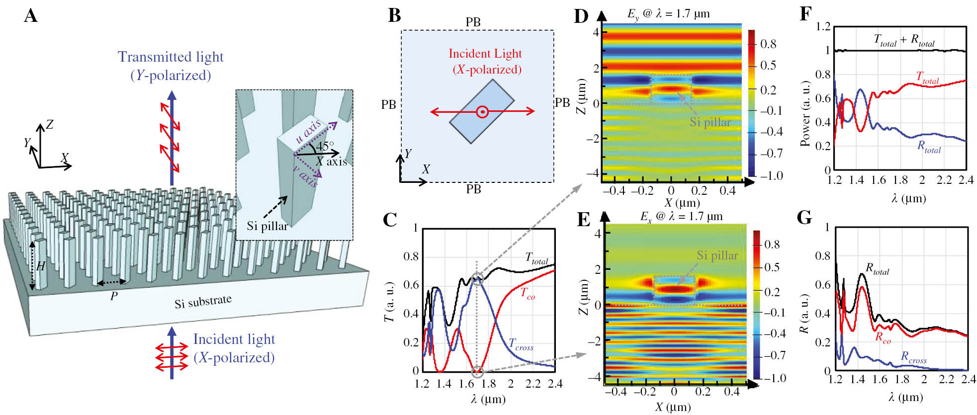
Schematic and design of Si metasurface-based HWP.
(A) 3D schematic of the metasurface-based HWP, which is composed of an array of identical Si nano-pillars. The inset is an enlarged view of a Si pillar. The angle between the long-axis (u-axis) of the pillar and the X-axis is 45°. (B) Top view of the Si nano-pillar unit cell in FDTD simulation. PB, periodic boundary. (C) Simulated transmittance spectra of a HWP with L=400 nm, W=200 nm, and H=1700 nm at λ=1.2 to 2.4 μm. Amplitude of the electric field along the (D) Y-axis and (E) X-axis at λ=1.7 μm. (F) Total transmittance (Ttotal) and reflectance (Rtotal) spectra of the HWP. (G) Simulated reflectance spectra of the HWP.
The performance of the metasurface-based HWP is studied in detail by commercial simulation software (FDTD Solutions, Lumerical Inc., Vancouver, British Columbia, Canada, https://www.lumerical.com/products/fdtd/). Figure 1B illustrates the top view of the Si nano-pillar unit cell. Four periodic boundaries (PB) at the X- and Y-axes and two perfectly matched layer absorbing boundaries at the Z-axis are employed. For the simulations in this work, the length of the unit cell is fixed at 1000 nm and the sidewall angle of the simulated Si pillar is 90° (not shown in this figure) unless otherwise mentioned. A plane-wave light source with the E-field polarized along the X-axis is incident toward the positive Z direction from the substrate. Therefore, the co- and cross-polarized light indicate the transmitted light that polarized along the X- and Y-axes, respectively.
The simulated transmittance spectra of an HWP with L=400 nm, W=200 nm, and H=1700 nm at the wavelengths (λ) ranging from 1.2 to 2.4 μm are plotted in Figure 1C. The total transmittance (Ttotal) equals the sum of the co-polarized (Tco) and the cross-polarized (Tcross) transmittances. It can be observed that Tco has minimum values (close to 0) at the wavelengths near 1.35 and 1.7 μm, at which Tcross has peak values of around 0.6. This indicates that the nano-pillars with the as-designed geometric parameters provide π phase retardation at two wavelength ranges. One possible problem of using a relatively large pillar height of 1700 nm is that it might make the etching process more challenging. However, this should not be a concern for the flat optics fabrication platform in the Institute of Microelectronics (IME), A*STAR, as a dedicated dry etching process has been developed for the formation of Si nano-pillars with a height of up to a few microns and an aspect ratio (width over height) of less than 1:10.
The normalized electric field distributions for cross- and co-polarized transmitted light at λ=1.7 μm are plotted in Figure 1D and E, respectively. It can be clearly seen that the electric field amplitude along the Y-axis (Ey) is very strong for the transmitted light, whereas that along the X-axis (Ex) becomes negligible after passing through the metasurface. One sees from Figure 1C that Ttotal is not 1 in the wavelength range, indicating the loss of the incident light when transmitting through the metasurface. This should be mainly due to light reflection as presented in Figure 1F, which shows that Ttotal nearly equals 1 minus the total reflected light power (Rtotal). In addition, it is worth to point out that the reflected light is not necessarily co-polarized. As shown in Figure 1G, a minor part of the light reflected from the metasurface can also be cross-polarized.
It is well known that fabrication process variations could not be avoided in the CMOS fabrication line. Therefore, it is imperative to study the impact of process variations on device performances for mass production. Next, the impact of variation in L, W, and H of Si pillars on the performance of the HWP is investigated by FDTD simulation using the same model as above. Figure 2A and B show the Tcross and Tco spectra of the HWP, respectively, with L varying from 380 to 420 nm. The black dashed arrow indicates the direction of increasing L with a step of 10 nm. W and H of the pillar are fixed at 200 and 1700 nm, respectively. It can be observed that increasing L leads to red-shift of both Tcross and Tco spectra. In addition, the shift of the longer valley wavelength (λlong) is larger than that of the shorter valley wavelength (λshort), as shown in Figure 2B. The shift of both λlong and λshort as a function of L is plotted in Figure 2C. A linear regression fitting of the points with a least-squares method yields the λ-shift rates (Δλ/ΔL) of 2.3 and 0.5 nm/nm for λlong and λshort, respectively.
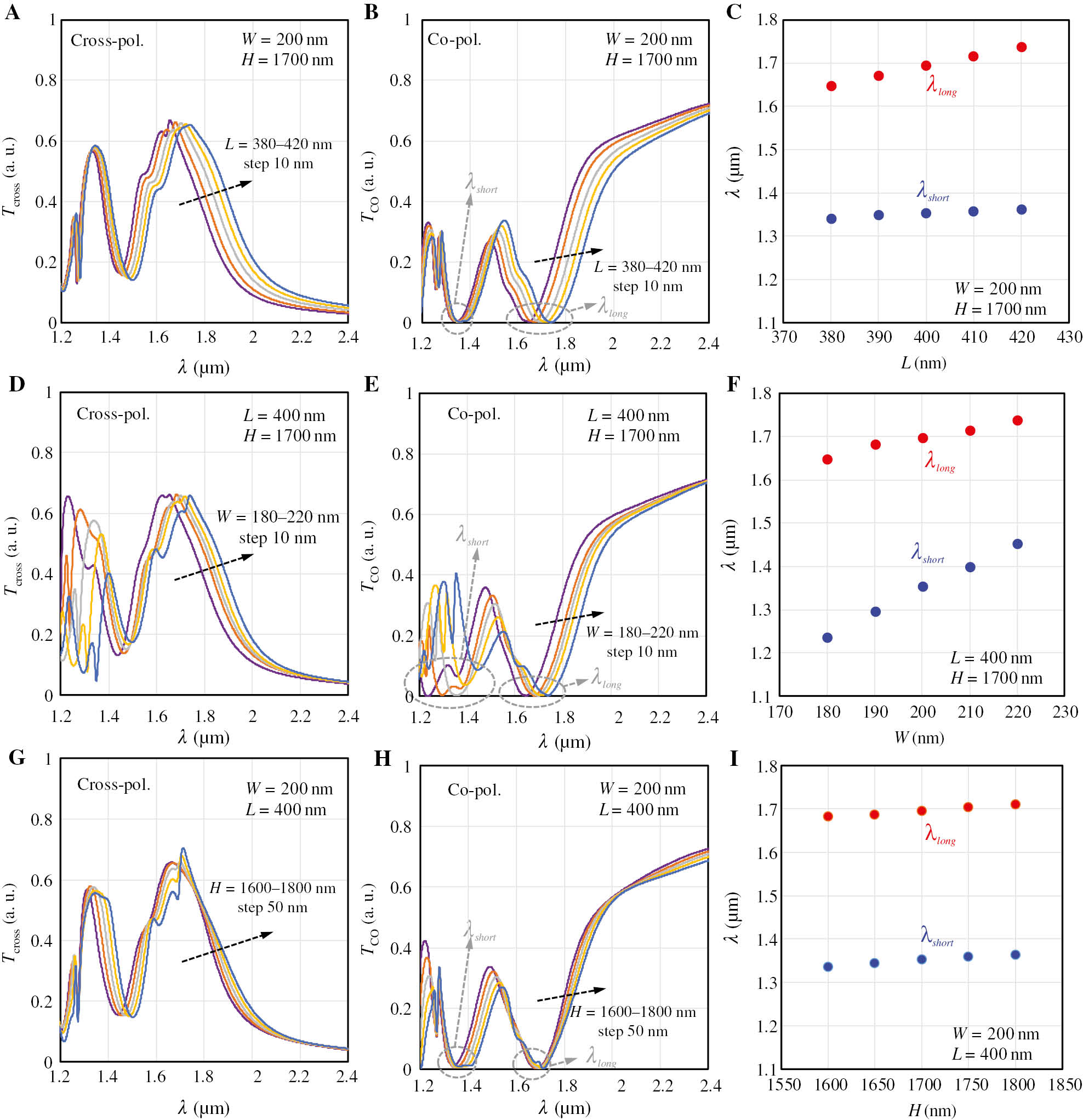
Device performance investigation considering geometric changes due to fabrication process variation.
(A) Tcross and (B) Tco spectra of the HWP, with L varying from 380 to 420 nm. The black dashed arrow indicates the direction of increasing L with a step of 10 nm. (C) The shift of λlong and λshort as a function of L. (D) Tcross and (E) Tco spectra of the HWP, with W varying from 180 to 220 nm. (F) The shift of λlong and λshort as a function of W. (G) Tcross and (H) Tco spectra of the HWP, with H varying from 1600 to 1800 nm with a step of 50 nm. (I) The shift of λlong and λshort as a function of H.
Similarly, the impacts of changing W on the Tcross and Tco spectra of the HWP are simulated and plotted in Figure 2D–F. W increases from 180 to 220 nm with a step of 10 nm, whereas L and H are fixed at 400 and 1700 nm, respectively. It can be observed in Figure 2E that increasing W leads to a more significant impact on λshort rather than λlong. The linear fitting of the data points in Figure 2F shows a λ-shift rate (Δλ/ΔW) of 2.1 nm/nm for λlong, whereas that for λshort is 5.4 nm/nm. Finally, the increase of H also leads to the red-shift of Tcross and Tco, as shown in Figure 2G and H, respectively. Different from changing W or L, the increase of H yields a similar λ-shift rate (Δλ/ΔH) of ~0.15 nm/nm for both Tcross and Tco, as shown in Figure 2I.
3 Results and discussion
The HWPs were fabricated on a 12-inch Si (100) wafer using the multiple-projects-wafer process for flat-optics in IME, A*STAR. The designed metasurface was patterned by a 193-nm DUV immersion scanner and subsequently etched by an inductively coupled plasma etcher. The remaining organic mask was eventually stripped in O2 plasma. A photograph of the fabricated 12-inch Si metasurface wafer is shown in Figure 3A. The size of the HWP in each die is 3.6 mm×3.6 mm. In conventional optics, the waveplates have typical diameters of 1 to 2 inches. It should be noted that the relatively small size of the device in this work is for proof-of-concept demonstration purpose. In fact, HWPs with much larger size can be realized using the DUV lithography process. The HWPs with diameters of less than 1 inch can be directly patterned within a single die as the die size of the immersion lithography tool is 26 mm×33 mm. Besides, the devices with diameters larger than 1 inch can also be realized by the field-stitching patterning technology [24]. The white dashed squares highlight nine of the selected dies at different wafer locations for optical characterizations, which will be discussed later. Figure 3B shows the tilted-view scanning electron microscopy (SEM) image of the HWP at the central die D(0,0). The zoomed-in view of a single Si pillar is shown in Figure 3C. The L, W, and H of the Si pillar are measured to be around 400, 217, and 1656 nm, respectively. Figure 3D shows the top-view SEM image of the array. It can be seen that the Si pillars are rotated 45° from the X-axis and the pitch between pillars is 1000 nm.
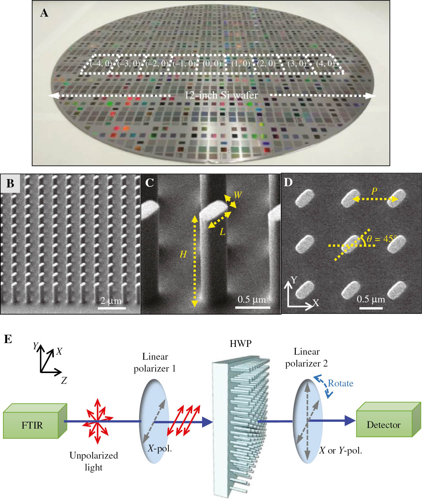
Fabrication results and characterization setup of the Si metasurface-based HWP.
(A) Photograph of the fabricated 12-inch Si metasurface wafer. The white dashed squares highlight nine of the selected dies at different wafer locations for optical characterizations. (B) Tilted-view SEM image of the Si pillar array at D(0,0). (C) Zoomed-in view of a single Si pillar. (D) Top view of the Si pillars. (E) Schematic of the optical characterization system used for HWP measurement. The system comprises an FTIR source, two linear polarizers, and one photodetector.
Optical characteristics of the metasurface-based HWPs were measured by a Fourier transform infrared (FTIR) spectrometer. As illustrated in Figure 3E, the measurement system is composed of an FTIR light source, two linear polarizers, and one photodetector working at short-wave infrared wavelengths. Unpolarized light comes from the FTIR light source. Polarizer 1 is fixed at X-polarization so that the transmitted light is linearly polarized along the X-axis of the HWP. Therefore, the cross- or co-polarization transmittances of the HWPs can be obtained by setting the linear polarizer 2 at Y- or X-polarizations, respectively. Tcross and Tco of the HWPs are then obtained by normalizing the as-measured transmittance spectra to those of a bare Si wafer.
The Tcross and Tco spectra of the HWP at D(0,0) at the wavelengths ranging from 1.2 to 2.4 μm are plotted in Figure 4A and B, respectively. A Tco minimum value of 0.032 is realized at λ=1.726 μm based on experimental data. At the same wavelength, Tcross shows a peak value of 0.621. The polarization conversion efficiency (Ec), defined as Ec=Tcross/(Tcross+Tco), as a function of λ is plotted in Figure 4C. An efficiency of around 95% is achieved at the wavelength near 1.726 μm. It should be noted that Ec in this work is referred to the transmitted light through the metasurface. The efficiency becomes around 62% if it is normalized to the total light power that is incident to the metasurface considering the loss from surface reflection. The black dashed lines in Figure 4A–C are the simulated spectra of the HWP using the pillar geometric parameters measured by SEM. A decent matching between the simulated and the experimental results can be observed. Besides Tco, Tcross, and Ec, the phase retardation is another figure of merit for HWPs. There are various methods to measure the phase retardation of waveplates [5], [9], [25]. Additional efforts can be input to accurately measure the phase retardation of the as-fabricated HWPs, which can be the subject of future works.
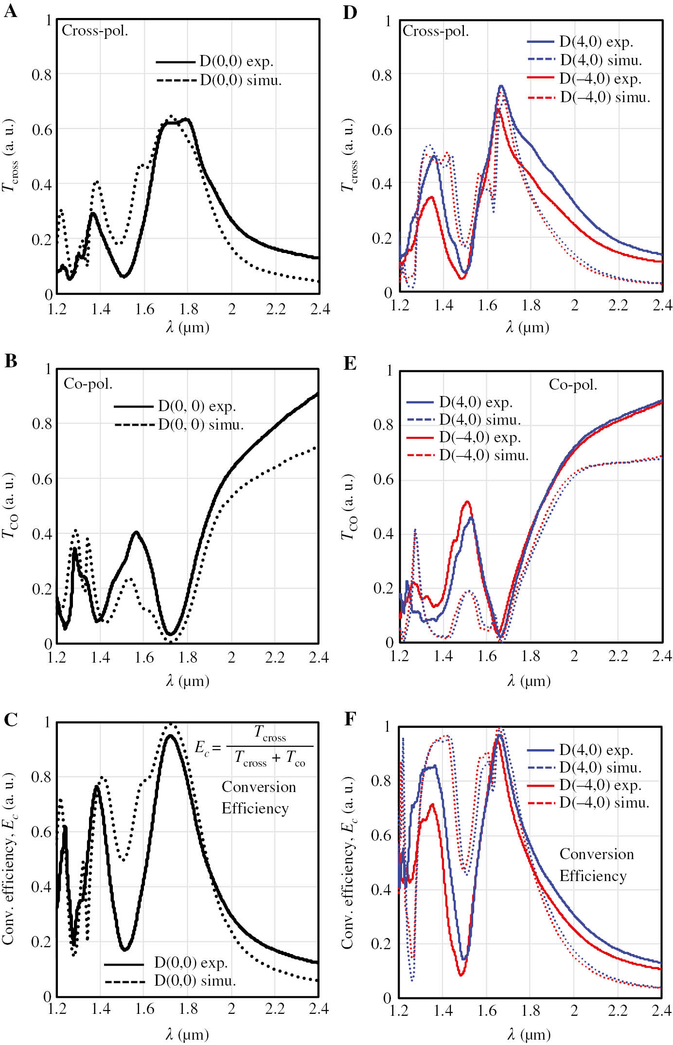
Characterization results of Si metasurface-based HWP.
Experimental results of (A) Tcross, (B) Tco, and (C) Ec spectra of the HWP at D(0,0). A Tcross value of 0.621 and a Tco value of 0.032 are achieved at λ=1.726 μm, which corresponds to an Ec of 95.1%. Experimental results of (D) Tcross, (E) Tco, and (F) Ec spectra of the HWP at D(4,0) and D(−4,0). Peak Ec values of 97.1% and 95.1% are realized for the HWPs at D(4,0) and D(−4,0), respectively. Dashed lines are the simulation results based on the measured parameters.
Additional optical characterizations on the HWPs located near the wafer edge were also performed, as presented in Figure 4D–F. The blue and red solid lines represent the measurement results for the HWPs at D(4,0) and D(−4,0), respectively. The minimum Tco value of the HWP at D(4,0) is 0.023 at λ=1.658 μm, and at D(−4,0) the value is 0.035 at λ=1.646 μm. It can be found that the Tcross and Tco spectra are shifted as compared to that at D(0,0). This should be due to the variations in geometric parameters of the Si pillars located at the wafer edge. The SEM measurement shows that the L, W, and H values for the HWP at D(4,0) are 371, 202, 2000 nm, respectively, and those values become 369, 202, and 1939 nm for the HWP at D(−4,0). The dashed lines in Figure 4D and E are the simulated Tcross and Tco spectra based on the measured critical dimension (CD). It can be seen that the peak wavelengths of Tcross and valley wavelengths of Tco are both near 1.65 μm, which are close to the experimental results. Figure 4F shows the experimental and simulated Ec of the HWPs at D(4,0) and D(−4,0). The peak Ec value of 97.1% for the HWP at D(4,0) and 95.1% for that at D(−4,0) are experimentally demonstrated.
It should be noted that the peak Tcross values of around 70% are lower than some of the previous demonstrations. For example, Kruk et al. [5] and Arbabi et al. [9] reported Si metasurface-based HWPs on glass/fused silica substrates with the transmission of around 90%. In these works, the implementation of glass/fused silica substrates reduces reflection loss of the HWP, resulting in a higher transmission. The Tcross value of our device can be improved by using the glass wafer substrate. It is worth noting that the devices in [5], [9] are realized on small pieces of substrates. However, the large-scale fabrication of metasurfaces on 12-inch non-Si wafers, for example, glass, fused silica, and sapphire, using the advanced CMOS processing facilities is more complicated. As reported in [20], [21], [22], metasurfaces can be formed on 12-inch glass wafers by a layer-transfer method, in which the metasurfaces are fabricated on standard Si wafers, followed by a special wafer bonding process to transfer them onto the glass wafers. A more intuitive way is to directly fabricate nanostructures on 12-inch non-Si wafers using CMOS infrastructures. Although progress has been made on realizing metasurfaces on small size wafers [18], the direct processing of 12-inch non-Si wafers using advanced CMOS facilities is much more challenging. For example, specific requirements of the stress, transparency, thermal conductivity, electrostatic chucking/de-chucking capabilities of the wafers have to be considered during the large-scale fabrication process. Therefore, although there is degradation in transmission, the direct fabrication of metasurfaces on 12-inch Si substrates significantly reduces the process time, cost, and complexity as compared with that on non-Si wafers.
Further investigation on the device performance uniformity across the fabricated wafer is performed by characterizing Tcross and Tco of the HWPs at the nine selected dies (0, 0), (±1, 0), (±2, 0), (±3, 0), and (±4, 0), as plotted in Figure 5A and B. The peak values of the Tcross spectra range from 0.627 to 0.768, with an average of 0.69 and a standard deviation of 0.053, as shown in Figure 5C. In addition, it can be seen from Figure 5D that the valley values of the Tco spectra are distributed with a mean of 0.032±0.005. The Ec of the HWPs are also calculated to be 95.6%±0.8%. Meanwhile, the wavelength shift of the HWPs across the wafer is studied by analyzing the Tco valley values of the devices at different dies, as presented in Figure 5E. The mean and standard deviation of the wavelength valley values are 1.72 and 0.04 μm, respectively.
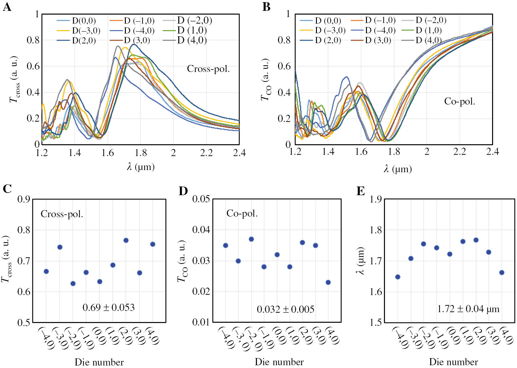
Wafer-level device performance analysis.
(A) Tcross and (B) Tco spectra of the HWPs from the nine selected dies at different wafer locations. (C) Peak Tcross and (D) valley Tco values of the HWPs. (E) The valley wavelength of Tco for the selected HWPs.
The performance non-uniformity of the HWPs should be mainly contributed by the variation in geometric parameters of the nanostructures, that is, L, W, and H variations of the Si pillars. Generally, the CD variations are mostly from the lithography and etching process. It is worth to mention that the 193-nm DUV immersion scanner has a relatively small CD variation range, defined as the difference between the maximum and the minimum CD for the same metasurface design, over the entire 12-inch wafer. This can be seen from [13], where a wafer-level CD variation range of around 2 to 4 nm was reported. Thus, most of the CD bias of the fabricated wafer should be originated from the etching process. The impacts of etching bias on the geometric parameters of the Si pillar are twofolds: (i) the CD bias of L and W should be attributed to the non-uniform lateral etching across the wafer. This can be improved by further optimizing the etching recipes, for example, increasing the pillar sidewall passivation during the plasma etching process; (ii) the etching depth (H) bias between different HWPs should be caused by the non-uniformity in etching rates at different wafer locations. One possible way to solve this problem is to implement an etch stop layer, for example, SiO2, beneath the metasurface. Further work includes the enhancement of the wafer-level CD uniformity of flat optics devices.
4 Conclusion
In summary, the metasurface-based HWPs are demonstrated on a 12-inch CMOS platform, featuring ultrathin device thickness and the possibility of being monolithically integrated with other optical components. The 3D FDTD simulation results indicate that the variation in L, W, and H of the Si pillar leads to wavelength shift of the HWP transmittance spectra. In addition, Tcross, Tco, and Ec of the HWPs at different wafer locations are experimentally measured to be 0.69±0.053, 0.032±0.005, and 95.6±0.8%, respectively, at the wavelength of around 1.7 μm. The wafer-level uniformity of device performance can be further enhanced by improving the process conditions. This work paves the way for mass production of flat optics using the mature CMOS fabrication facilities.
Acknowledgments
This work received RIE2020 Advanced Manufacturing and Engineering (AME) Domain’s Core Funds: SERC Strategic Funds (A1818g0028). The authors would like to thank Dr. Yu Li for technical discussion. The appreciation extends to Dr. Dongdong Li, Dr. Ying Lin, Keng Heng Lai, and Larry Sim for assistance on the lithography process.
References
[1] Lavrentovich MD, Sergan TA, Kelly JR. Switchable broadband achromatic half-wave plate with nematic liquid crystals. Opt Lett 2004;29:1411–3.10.1364/OL.29.001411Search in Google Scholar PubMed
[2] Abuleil MJ, Abdulhalim I. Tunable achromatic liquid crystal waveplates. Opt Lett 2014;39:5487–90.10.1364/OL.39.005487Search in Google Scholar PubMed
[3] Wang L, Lin XW, Hu W, et al. Broadband tunable liquid crystal terahertz waveplates driven with porous graphene electrodes. Light Sci Appl 2015;4:e253.10.1038/lsa.2015.26Search in Google Scholar
[4] Yu N, Genevet P, Kats MA, et al. Light propagation with phase discontinuities: generalized laws of reflection and refraction. Science 2011;334:333–7.10.1126/science.1210713Search in Google Scholar PubMed
[5] Kruk S, Hopkins B, Kravchenko II, Miroshnichenko A, Neshev DN, Kivshar YS. Invited article: broadband highly efficient dielectric metadevices for polarization control. APL Photon 2016;1:030801.10.1063/1.4949007Search in Google Scholar
[6] Ding F, Wang Z, He S, Shalaev VM, Kildishev AV. Broadband high-efficiency half-wave plate: a supercell-based plasmonic metasurface approach. ACS Nano 2015;9:4111–9.10.1021/acsnano.5b00218Search in Google Scholar PubMed
[7] Jiang ZH, Lin L, Ma D, et al. Broadband and wide field-of-view plasmonic metasurface-enabled waveplates. Sci Rep 2014;4:7511.10.1038/srep07511Search in Google Scholar PubMed PubMed Central
[8] Yang Y, Wang W, Moitra P, Kravchenko II, Briggs DP, Valentine J. Dielectric meta-reflect array for broadband linear polarization conversion and optical vortex generation. Nano Lett 2014;14:1394–9.10.1021/nl4044482Search in Google Scholar PubMed
[9] Arbabi A, Horie Y, Bagheri M, Faraon A. Highly efficient polarization control using subwavelength high contrast transmit arrays. Proc SPIE 2015;9372:93720H.10.1117/12.2079559Search in Google Scholar
[10] Backlund MP, Arbabi A, Petrov PN, et al. Removing orientation-induced localization biases in single-molecule microscopy using a broadband metasurface mask. Nat Photon 2016;10:459–62.10.1038/nphoton.2016.93Search in Google Scholar PubMed PubMed Central
[11] Magden ES, Li N, Raval M, et al. Transmissive silicon photonic dichroic filters with spectrally selective waveguides. Nat Commun 2018;9:3009.10.1038/s41467-018-05287-1Search in Google Scholar PubMed PubMed Central
[12] Shtyrkova K, Callahan PT, Li N, et al. Integrated CMOS-compatible Q-switched mode-locked lasers at 1900nm with an on-chip artificial saturable absorber. Opt Express 2019;27:3542–56.10.1364/OE.27.003542Search in Google Scholar PubMed
[13] Singh N, Xin M, Vermeulen D, et al. Octave-spanning coherent supercontinuum generation in silicon on insulator from 1.06μm to beyond 2.4μm. Light Sci Appl 2018;7:17131.10.1038/lsa.2017.131Search in Google Scholar PubMed PubMed Central
[14] Poulton CV, Byrd MJ, Raval M, et al. Large-scale silicon nitride nanophotonic phased arrays at infrared and visible wavelengths. Opt Lett 2017;42:21–4.10.1364/OL.42.000021Search in Google Scholar PubMed
[15] Li N, Su Z, Purnawirman, et al. Athermal synchronization of laser source with WDM filter in a silicon photonics platform. Appl Phys Lett 2017;110:211105.10.1063/1.4984022Search in Google Scholar PubMed PubMed Central
[16] Xu Z, Dong Y, Tseng CK, et al. CMOS-compatible all-Si metasurface polarizing bandpass filters on 12-inch wafers. Opt Express 2019;27:26060–9.10.1364/OE.27.026060Search in Google Scholar PubMed
[17] Hu T, Tseng CK, Fu YH, et al. Demonstration of color display metasurfaces via immersion lithography on a 12-inch silicon wafer. Opt Express 2018;26:19548–54.10.1364/OE.26.019548Search in Google Scholar PubMed
[18] She A, Zhang S, Shian S, Clarke DR, Capasso F. Large area metalenses: design, characterization, and mass manufacturing. Opt Express 2018;26:1573–85.10.1364/OE.26.001573Search in Google Scholar PubMed
[19] Zhong Q, Li Y, Hu T, et al. 1550nm-Wavelength Metalens Demonstrated on 12-Inch Si CMOS Platform. In 2019 IEEE 16th International Conference on Group IV Photonics (GFP), Lisbon, Portugal, Vol. 1949–209X, 2019:1–2.10.1109/GROUP4.2019.8925873Search in Google Scholar
[20] Hu T, Zhong Q, Li N, et al. Demonstration of a-Si metalenses on a 12-inch glass wafer by CMOS-compatible technology. arXiv e-prints 2019;1906:11764.Search in Google Scholar
[21] Xu Z, Dong Y, Fu YH, et al. Embedded dielectric metasurface based subtractive color filter on a 300 mm glass wafer. In: Conference on Lasers and Electro-Optics, OSA Technical Digest (Optical Society of America, 2019), p. STh1O.4.10.1364/CLEO_SI.2019.STh1O.4Search in Google Scholar
[22] Li N, Fu YH, Dong Y, et al. Large-area pixelated metasurface beam deflector on a 12-inch glass wafer for random point generation. Nanophotonics 2019;8:1855–61.10.1515/nanoph-2019-0208Search in Google Scholar
[23] Schonbrun E, Seo K, Crozier KB. Reconfigurable imaging systems using elliptical nanowires. Nano Lett 2011;11:4299–303.10.1021/nl202324sSearch in Google Scholar PubMed
[24] Harris PD, McCallum M, Muir D, Hughes G, Pinkney S. Practical DUV lithography for the optoelectronics market. Proc SPIE 2003;5038:910–7.10.1117/12.482810Search in Google Scholar
[25] Zhang P, Tan Y, Liu W, Chen W. Methods for optical phase retardation measurement: a review. Sci China Technol Sci 2013;56:1155–63.10.1007/s11431-013-5207-4Search in Google Scholar
©2019 Zhengji Xu et al., published by De Gruyter, Berlin/Boston
This work is licensed under the Creative Commons Attribution 4.0 Public License.
Articles in the same Issue
- Reviews
- Optical binding of nanoparticles
- Recent advances in nano-photonic techniques for pharmaceutical drug monitoring with emphasis on Raman spectroscopy
- Optically responsive delivery platforms: from the design considerations to biomedical applications
- Research Articles
- Beyond dipolar Huygens’ metasurfaces for full-phase coverage and unity transmittance
- Bound states in the continuum and strong phase resonances in integrated Gires-Tournois interferometer
- Improving the efficiency of silicon solar cells using in situ fabricated perovskite quantum dots as luminescence downshifting materials
- Structural and optical impacts of AlGaN undershells on coaxial GaInN/GaN multiple-quantum-shells nanowires
- Surface-plasmon-polariton-driven narrow-linewidth magneto-optics in Ni nanodisk arrays
- Broadband multi-wavelength optical sensing based on photothermal effect of 2D MXene films
- Tailoring the spatial localization of bound state in the continuum in plasmonic-dielectric hybrid system
- High-speed multiplane structured illumination microscopy of living cells using an image-splitting prism
- Si metasurface half-wave plates demonstrated on a 12-inch CMOS platform
- Implementation of on-chip multi-channel focusing wavelength demultiplexer with regularized digital metamaterials
- Imprinted plasmonic measuring nanocylinders for nanoscale volumes of materials
- Hydrophobin HGFI–based fibre-optic biosensor for detection of antigen–antibody interaction
- Enhanced terahertz emission from imprinted halide perovskite nanostructures
- Realization of complex conjugate media using non-PT-symmetric photonic crystals
- Selective tuning of optical modes in a silicon comb-like photonic crystal cavity
- Phase-coupled simultaneous coherent perfect absorption and controllable hot-electron photodetection in Schottky junction metamaterial
- Landau quantisation of photonic spin Hall effect in monolayer black phosphorus
- Near-field spectrum retrieving through non-degenerate coupling emission