
Synthesis of few-layer 2H-MoSe2 thin films with wafer-level homogeneity for high-performance photodetector
-
Tian-Jun Dai
 ,
Yu-Chen Liu
,
Yu-Chen Liu
 ,
Dan Xie
und
Yan-Rong Li
,
Dan Xie
und
Yan-Rong Li

Abstract
The unique structural and physical properties of two-dimensional (2D) atomic layer semiconductors render them promising candidates for electronic or optoelectronic devices. However, the lack of efficient and stable approaches to synthesize large-area thin films with excellent uniformity hinders their realistic applications. In this work, we reported a method involving atomic layer deposition and a chemical vapor deposition chamber to produce few-layer 2H-MoSe2 thin films with wafer-level uniformity. The reduction of MoO3 was found indispensable for the successful synthesis of MoSe2 films due to the low vaporization temperature. Moreover, a metal-semiconductor-metal photodetector (PD) was fabricated and investigated systematically. We extracted an ultrahigh photoresponsivity approaching 101 A/W with concomitantly high external quantum efficiency up to 19,668% due to the produced gain arising from the holes trapped at the metal/MoSe2 interface, the band tail state contribution, and the photogating effect. A fast response time of 22 ms was observed and attributed to effective nonequilibrium carrier recombination. Additionally, the ultrahigh photoresponsivity and low dark current that originated from Schottky barrier resulted in a record-high specific detectivity of up to 2×10¹³ Jones for 2D MoSe2/MoS2 PDs. Our findings revealed a pathway for the development of high-performance PDs based on 2D MoSe2 that are inexpensive, large area, and suitable for mass production and contribute to a deep understanding of the photoconductivity mechanisms in atomically thin MoSe2. We anticipate that these results are generalizable to other layer semiconductors as well.
1 Introduction
Nanomaterials are gaining intense interest in photodetection due to their large surface-to-volume ratios and low dimensions, which can yield higher light sensitivity than their bulk counterparts. The charge separation promoted by surface states is considered to be responsible for the prolonged photocarrier lifetime [1], resulting in a high photocurrent gain. Until now, by employing quantum dots (QDs) [2] and one-dimensional (1D) semiconducting nanostructures of ZrS2, CdS, and ZnO as sensitizers [3], [4], [5], high-performance photodetectors (PDs) have been demonstrated. However, the complexity in manipulation and poor uniformity of 1D/QD materials impede their realistic applications. Intriguingly, benefiting from the quantum confinement effects in the out-of-plane direction, two-dimensional (2D) materials are highly promising for high-performance optoelectronic devices, which are compatible with current thin-film microfabrication techniques appropriately. Although the extremely high electrical mobility (up to 200,000 cm2/v/s for both electrons and holes) [6] and vanishing effective mass render graphene a promising candidate for high-speed photodetection, the responsivity of graphene-based PDs is far from satisfactory (~10−3 A/W) mainly due to its short photocarrier lifetime [7], low absorption ratio of incident light (~2%) [8], [9], and external quantum efficiency (EQE; 0.1–0.2%) [10]. Until recently, Zhang et al. demonstrated a hybrid graphene-ZnO PD with a high responsivity of up to 104 A/W [11] but with increasing fabrication complexity. Especially, PDs made from ultrathin 2D semiconducting transition metal dichalcogenides (TMDs), such as MoS2, WS2, MoSe2, and WSe2 [12], [13], [14], [15], can exhibit enhanced responsivity and selectivity compared to graphene-based devices due to their appropriate bandgaps (Eg ~1–2 eV).
The preparation of good-quality 2D layered materials with wafer-scale uniformity is an essential requirement for industry applications in optical devices. Until now, most experimental research focuses on 2D mechanical exfoliation from the bulk because of its low-cost and accessible high-quality samples. For example, a phototransistor based on a mechanically exfoliated single-layer MoS2 nanosheet with a responsivity of 7.5 mA/W was first reported by Yin et al. [16]. Afterward, a greatly enhanced responsivity of up to 880 A/W was achieved with similar device geometry due to the improved contact quality and carrier mobility [17] but at the cost of low response time (4 s). Moreover, Group IIIA metal chalcogenide 2D layered materials (GaSe and GaS) have also been produced by exfoliating high-performance PDs [18], [19]. However, scalable production is highly challenging for this approach due to the low throughput. Furthermore, the traditional technique, chemical vapor deposition (CVD), has shown great potential to generate high-quality 2D nanosheets used in optoelectronics. As one of the earliest used in PDs, CVD-grown monolayer MoSe2 crystals showed a fast response time of 60 ms but failed to realize an impressing responsivity [20]. Although the extremely high responsivity (3×10³ A/W) and fast photoresponse (59 μs) have been realized by employing bilayer WS2 as a photoactive layer synthesized via CVD recently [21], only few devices can be fabricated on a selected area because of the small lateral size of CVD products as well as the poor deposition repeatability, which is just suitable for fundamental research and proof-of-concept device fabrication. Additionally, 2D nanosheets prepared from other methods, such as pulsed laser deposition (PLD) [15], thermolysis synthesis [12], and magnetron sputtering [22], have also been employed in PDs. However, these devices usually exhibit inferior responsivities compared to those of CVD-based devices. Accordingly, there is an urgent need to develop a stable and efficient technique to prepare wafer-size 2D films with excellent continuity for high-performance optical devices.
Hereby, we produced a wafer scale of few-layer 2H-MoSe2 nanosheets with a homogeneous distribution via atomic layer deposition (ALD) and CVD methods. A metal-semiconductor-metal (MSM)-structured PD based on the as-prepared 2D film was fabricated and comprehensively investigated. Impressively, the device exhibited excellent optoelectronics characteristics, including an ultrahigh responsivity approaching 101 A/W (under laser illumination at λ=638 nm), which is 104 times higher than the first graphene-based PDs [10] and deterministically surpassing any of the reported values of 2D MoSe2-based PDs previously (~0.26 mA/W–97.1 A/W) [14], [20], [23], [24], a high specific detectivity of up to 2×10¹³ Jones, which represent the best values reported thus far for most 2D TMD (MoS2, MoSe2, WS2, etc.)-based PDs, and a surprisingly high EQE of 19,668%. Moreover, we also showed that the few-layer MoSe2 possesses extraordinary reliable photoswitching with a fast response speed (22 ms). The photoconductivity mechanisms were discussed in depth. These outstanding figures of merits observed in our MoSe2 device render the synthesized wafer-size 2D films quite interesting for high-performance optoelectronic applications.
2 Materials and methods
2.1 Synthesis of MoSe2 thin layer
Initially, MoO3 thin films with desired thickness (150 cycles) were deposited on SiO2 (285 nm)/Si substrates at 162°C by ALD with a growth rate of 0.76 Å/cycle using Mo(CO)6 and O2 plasma as reactants. Subsequently, the MoO3-coated substrate was transferred into the CVD chamber with an inner tube (1 inch in diameter) for MoSe2 synthesis. Se powder was put upstream at a lower temperature zone (245°C) for evaporation. First, the as-deposited MoO3 was heated to 220°C for 30 min under flowing H2 (20 sccm) and Ar (50 sccm) gas. Second, the sample was annealed in a selenium-rich environment with a gradually increased temperature from 220°C to 900°C at a ramping rate of 11.6°C/min and maintained for 30 min for selenization reaction (H2 10 sccm and Ar 50 sccm), during which the chamber pressure was maintained at 0.29 Torr. Finally, the heater was turned off and the sample was subsequently cooled to room temperature under a flowing Ar (50 sccm) atmosphere.
2.2 Transfer of MoSe2 onto fresh SiO2/Si substrate and transmission electron microscopy (TEM) grid
The as-synthesized MoSe2 2D films on SiO2 substrates were coated with polymethyl methacrylate (PMMA) by spin coating (3000 rpm for 30 s) followed by baking at 180°C for 10 min. After that, the samples were immersed in 10% HF solution to etch the SiO2 layer. Subsequently, the PMMA-supported MoSe2 films were washed using deionized water. Afterward, a fresh SiO2/Si substrate or a TEM grid was used to fish the PMMA-capped MoSe2 films. Finally, the PMMA films were removed using acetone and washed away by isopropyl alcohol.
2.3 Device fabrication
PD with an interdigital geometry was engineered and fabricated by conventional photolithography. The evaporation of Au (80 nm)/Ti (10 nm) interdigital electrodes was used to define the contacts, where the thin Ti layer can improve the adhesion of Au onto the top of the MoSe2 nanosheet. The device comprise 20 pairs of interdigital electrodes whose length, width, and spacing were 180, 5, and 5 μm, respectively, corresponding to the effective illumination area of 3.51×10⁻⁴ cm2. After fabrication, the device was annealed at 350°C for 5 min by rapid thermal annealing technique under N2 conditions to reduce contact resistance and remove the photoresist remnants.
2.4 Characterization
The surface morphology and thickness of the as-grown MoSe2 thin films were studied using optical microscopy and atomic force microscopy (AFM; Bruker Multimode 8; Bruker, Billerica, MA, USA). X-ray photoelectron spectroscopy (XPS; Kratos XSAM800, UK) using Al Kα radiation (144W, 12 mA, 12 kV) was employed to determine the elemental composition. All obtained spectra were calibrated to a C-1s electron peak at 284.6 eV. The Raman spectrum was acquired at room temperature with excitation laser lines of 514 nm and an incident laser power of 2 mW (Renishaw). Moreover, the nanostructure of MoSe2 was investigated using high-resolution TEM (HRTEM) analysis (Zeiss Libra 200 FE). In addition, photoelectric measurement was carried out using an Agilent 4155B semiconductor parameter analyzer under 638 nm laser illumination in air.
3 Results and discussion
Compared to monolayer films, few-layer MoSe2 with a bandgap range from 1.1 to 1.6 eV [25] are more promising for high-responsivity optoelectronic nanodevices due to its higher light absorption, reduced bandgap, and smaller sheet resistance arising from the higher density of states, in which the intralayer Mo-Se bonds are predominantly covalent, whereas adjacent layers are weakly held together by van der Waals forces, exhibiting three polymorphs/phases including 1T, 2H, and 3R (depending on Mo atom coordination and the stacking orders), as shown in Figure 1. The 2H phase is related to hexagonal symmetry (D4h) with a stacking sequence of AbA BaB (Figure 1A), whereas the 3R phase corresponds to rhombohedral symmetry, demonstrating a stacking of AbA CaC BcB (Figure 1B). In both cases, the Mo coordination is trigonal prismatic. Moreover, the stacking in the 1T layer produces the AbC AbC sequence (Figure 1C), which has a tetragonal symmetry and corresponds to an octahedral coordination of Mo atoms. It was found that 1T-MoSe2 exhibits an expanded interlayer spacing of 1.17 nm compared to that of 2H-MoSe2 (0.646 nm) [26]. The preferred phase is primarily determined by the d-electron count of Mo atoms [27].
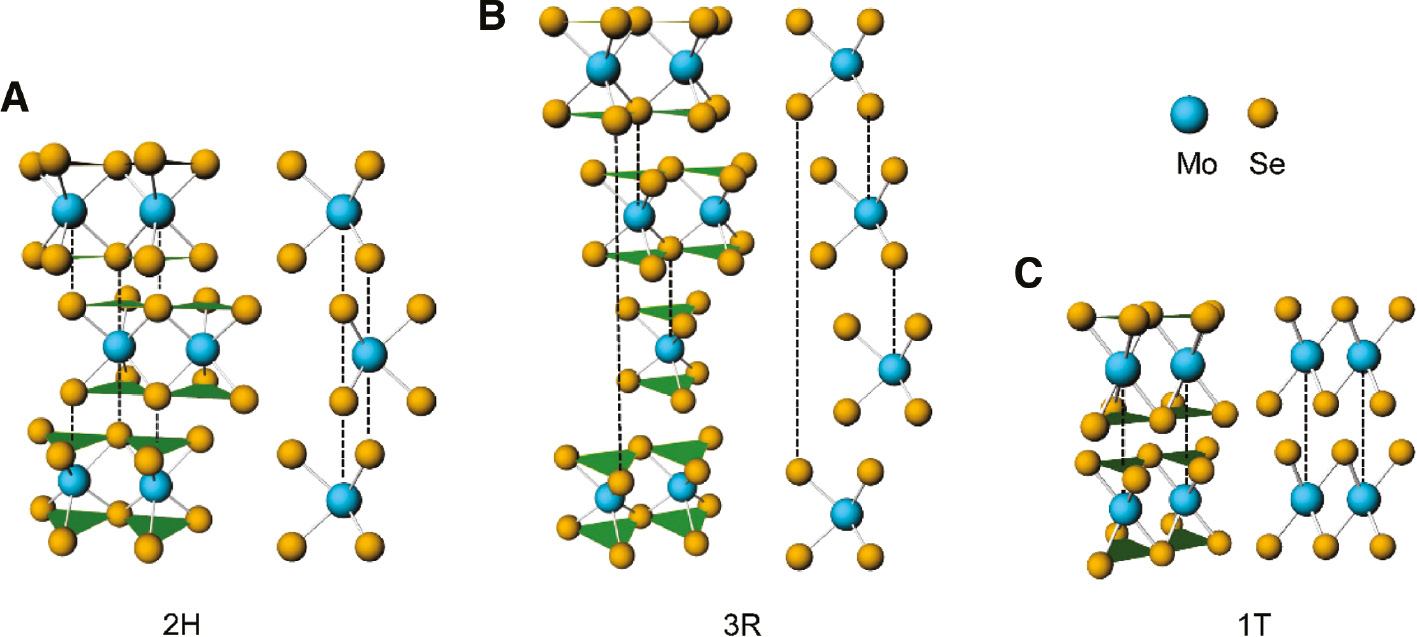
Schematic representation of the different polymorphs of a few-layer MoSe2 film: (A) 2H, (B) 3R, and (C) 1T.
Blue balls represent Mo atoms and the Se atoms are yellow.
Figure 2A typically illustrates the experimental setup for synthesizing thin MoSe2 layers. Selected MoO3 thin films of 150 cycles (~11.4 nm) were deposited on SiO2 (285 nm)/Si substrates using a standard ALD recipe [28]. Afterward, the synthesis of MoSe2 films from MoO3 was carried out in a two-zone CVD chamber, during which a mixture of H2/Ar was used as the carrier gas, where H2 acted as a reducing agent [23], which is indispensable in the selenization reaction [29], [30]. The chemical reaction occurring in the chamber is as follows:

Wafer-scale synthesis and morphology of MoSe2 film.
(A) Schematic representation of the synthesis of MoSe2 with ALD and a CVD method. MoO3 thin film with desired thickness was initially prepared via ALD and followed by a selenization process in CVD tube furnace. (B) Schematic representation of the temperature profile in a typical growth of MoSe2 thin films in a two-zone furnace. (C) Photograph of a bare SiO2 and the as-synthesized MoSe2. (D) Optical microscopy image of the as-grown MoSe2 thin film with a scratch made by a tweezer. (E) AFM height topography of MoSe2. The inset shows the height profile as measured along the red dotted line.
Note that the phase of SeO2 is a vapor as it is easily sublimated at temperatures above 350°C [31]. The selenization process is schematically shown in Figure 2B (see details in Materials and methods). It is noteworthy to point out that MoSe2 is not formed in the case of the direct selenization of MoO3 at 900°C without annealing at low-temperature phase. This is attributed to the vaporization of MoO3 before conversion to MoSe2. Accordingly, we employed a set of MoO3 samples of 90 ALD cycles for low-temperature annealing investigation. It was found that MoSe2 can be formed commendably at 900°C when the initial annealing temperature is below 250°C with flowing of a mixture of H2/Ar gas (Figure S1). This is ascribed to the reduction of MoO3 to MoO3–x, which has a higher vaporization temperature (~700°C) [32], resulting in a successful synthesis of MoSe2.
Figure 2C perspicuously shows the color contrast between a thin MoSe2 layer on 285 nm SiO2/Si and the bare substrate, where the sample with MoSe2 film displays a dark blue color compared to the violet substrate. It should be pointed out that the substrate size was limited by the diameter of the CVD tube furnace in our experiments currently. The homogeneous color observed in the optical image (Figure 2D) indicates a good uniformity of film thickness [20], [29]. Moreover, AFM was employed to determine the thicknesses of the synthesized MoSe2; as shown in Figure 2E (inset), the cross-sectional height profile reveals that the thickness of the sample is 8.6 nm, corresponding to 12 to 14 layers of MoSe2 while considering the 0.646 nm monolayer 2H-MoSe2 [26]. It was found that the surface roughness over a scanned area of 2×2 μm for MoSe2 is 0.42 nm, whereas the value for the ALD 150 cycles MoO3 is 0.95 nm before selenization (Figure S2), confirming the good uniformity.
The atomic structures and crystal quality of MoSe2 were characterized by TEM. An MoSe2 sample with a few millimeters in size was transferred to a TEM grid following a PMMA-assisted method. Figure 3 unambiguously shows a homogeneously well-structured as-prepared MoSe2 with large-scale continuous and 2H phase. Figure 3A displays a sketch of the crystal structure of the layered 2H-MoSe2. Both computational and experimental research indicate that the 2H stacking configuration of few-layer MoSe2 exhibits an AB1 stacking pattern where Mo atoms (top layer) are above Se atoms (bottom layer) [33]. Additionally, one layer of hexagonally packed Mo atoms with two atomic layers of Se atoms is covalently bonded on either side, forming a single layer of MoSe2. The low-magnification TEM image in Figure 3B shows a continuously transferred film, indicating the high quality of the synthesized specimen [34], and some residues are unavoidably caused by the transfer process, which are probably PMMA. Some wrinkles are evident on the edge of the film, as shown in Figure 3C, resulting from the mechanical scratching during the TEM sample preparation. The inset represents a selected area electron diffraction (SAED) pattern taken with an aperture size of ~160 nm containing diffraction points of (100) and (110) arranged in multiple hexagons, suggesting a polycrystalline nature of the MoSe2 layer stacking [35], [36]. A typical high-resolution TEM image for MoSe2 film is shown in Figure 3D, clearly revealing the layered structure. The magnified image in the inset shows a typical view of 13-layer MoSe2 nanosheets with clear lattice fringes identified at the wrinkled area, which is consistent with AFM characterization. The distance between two peaks in the intensity profile shown in Figure 3E is 0.65 nm (interlayer spacing), which matches well with the (002) plane of 2H-MoSe2 [26]. The hexagonal lattice structure with the lattice spacing of 0.28 and 0.16 nm assigned to the (100) and (110) planes was identified and the in-plane lattice constant of MoSe2 is measured to be 0.32 nm (Figure S3), which is in agreement with the value of theoretical calculation [37]. Figure 3F is the inverse fast Fourier fransformation (iFFT) image reconstructed from the area indicated by the square in Figure 3H, clearly showing a hexagonal shape. The corresponding atomic structure model of MoSe2 is well overlapped (see the inset) as well as another observed kind of contrast with triangular shape (Figure S4). Furthermore, a set of hexagonally arranged diffraction spots is clearly observed in the corresponding FFT image (Figure 3G), revealing that the few-layer MoSe2 exhibits the same stacking order for each layer.
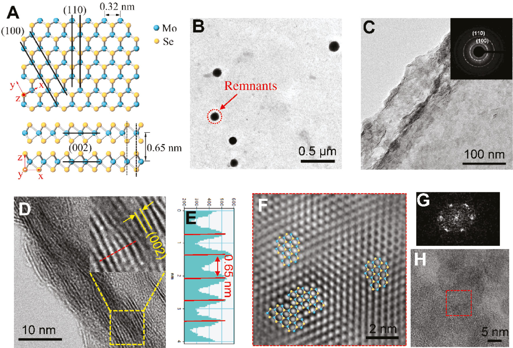
TEM characterization of MoSe2 atomic film on a TEM grid.
(A) Lattice configuration of MoSe2 with top and side views. Mo atoms are shown in blue and Se atoms are shown in yellow. (B) Low-magnification top-view TEM image of MoSe2 layers. Black dots were unavoidably produced during the transfer onto the TEM grid, representing the residues (PMMA). (C) Magnified view of the sample with an inset showing the SAED pattern of the polycrystalline film. Some wrinkles are observed on the edge of the film. (D) Typical HRTEM image of the few-layer MoSe2 film. (E) Line intensity profile of the red dot line drawn in D. (G and F) Corresponding FFT and iFFT images of the region indicated by squares in H, respectively.
The composition and chemical and electronic structures of the samples were investigated by performing a series spectroscopic characterizations. Figure 4A displays the vibrational normal modes of the 2H-MoSe2. The A1g mode denotes the Se atom vibration out of the basal plane and exhibits a blue shift with increasing layer number due to the interlayer interaction [38], [39]. In contrast, the E2g1 mode, which displays a red shift with increasing thickness, is caused by the vibration of Mo and Se atoms in the basal plane. Another mode, B2g1, is a shear mode corresponding to the vibration of two rigid layers against each other and is inactive in bulk and monolayer MoSe2 but can be observed in few layers due to the breakdown of translation symmetry [40]. The Raman spectra in Figure 4B show very little variation between five different points (marked in the inset) tested, further proving the uniformity of MoSe2 film. Except for the Si peak at 520 cm−1, three characteristic peaks are located at 240.8, 290.0, and 353.8 cm−1, corresponding to mode, mode and modethe A1g, E2g1, and B2g1 modes, respectively. The presence of the B2g1 mode in MoSe2 further confirms the few-layer structure nature, which is in good agreement with the TEM results. Furthermore, the homogeneity of the synthesized MoSe2 film was further verified by the Raman intensity mapping for the A1g mode (Figure S5). In addition, XPS was employed to characterize the chemical states of the samples. As shown in Figure 4C, two elements present in the spectra acquired Mo and O, and the peaks at 235.9 and 232.8 eV are attributed to the doublet Mo 3d3/2 and Mo 3d5/2 binding energies, respectively, corresponding to the fully oxidized Mo6+ state. Besides, the O 1s peak is observed at 530.5 eV. All of these results are consistent with the reported values for MoO3 [41]. After selenization, without changing the energy difference (Δ=3.1 eV) between the two peaks, Mo 3d3/2 shifted to 232.0 eV and Mo 3d5/2 shifted to 228.9 eV, respectively (Figure 4D), confirming that molybdenum is in its Mo(IV) state, and the binding energies of Se 3d5/2 and 3d3/2 are 54.4 and 55.3 eV, indicating the -2 oxidation chemical state for Se, in agreement with the values obtained in other MoSe2 systems [23], [31], confirming that the MoO3 thin films have been successfully converted into MoSe2. All the results unequivocally demonstrate that the as-synthesized sample is pure 2H-MoSe2 with good crystalline quality.

Structural and compositional investigations of the as-grown samples.
(A) Schematic representation of two Raman active and one inactive vibration modes in 2H-MoSe2 with the relative labels indicated for each mode. Blue and yellow balls represent Mo and Se atoms, respectively. (B) Raman spectra taken from the as-synthesized few-layer MoSe2 for five measurement points (inset). (C) High-resolution XPS spectra of MoO3 film, where the Mo 3d and O 1s binding energies are identified. (D) XPS measurements for the Mo 3d and Se 3d core levels of the synthesized MoSe2 film.
To investigate the photoelectrical properties of our synthesized few-layer MoSe2, Schottky PD was fabricated in a back-to-back MSM geometry that can lower the dark current, boosting the photosensitivity [12]. As illustrated schematically in Figure 5A, standard photolithographic and metal evaporation techniques were employed to produce the interdigital electrodes (10 nm Ti and 80 nm Au) as Schottky contacts. The electrical measurements were performed at room temperature under 638 nm laser illumination and the corresponding photoelectric behavior was recorded.
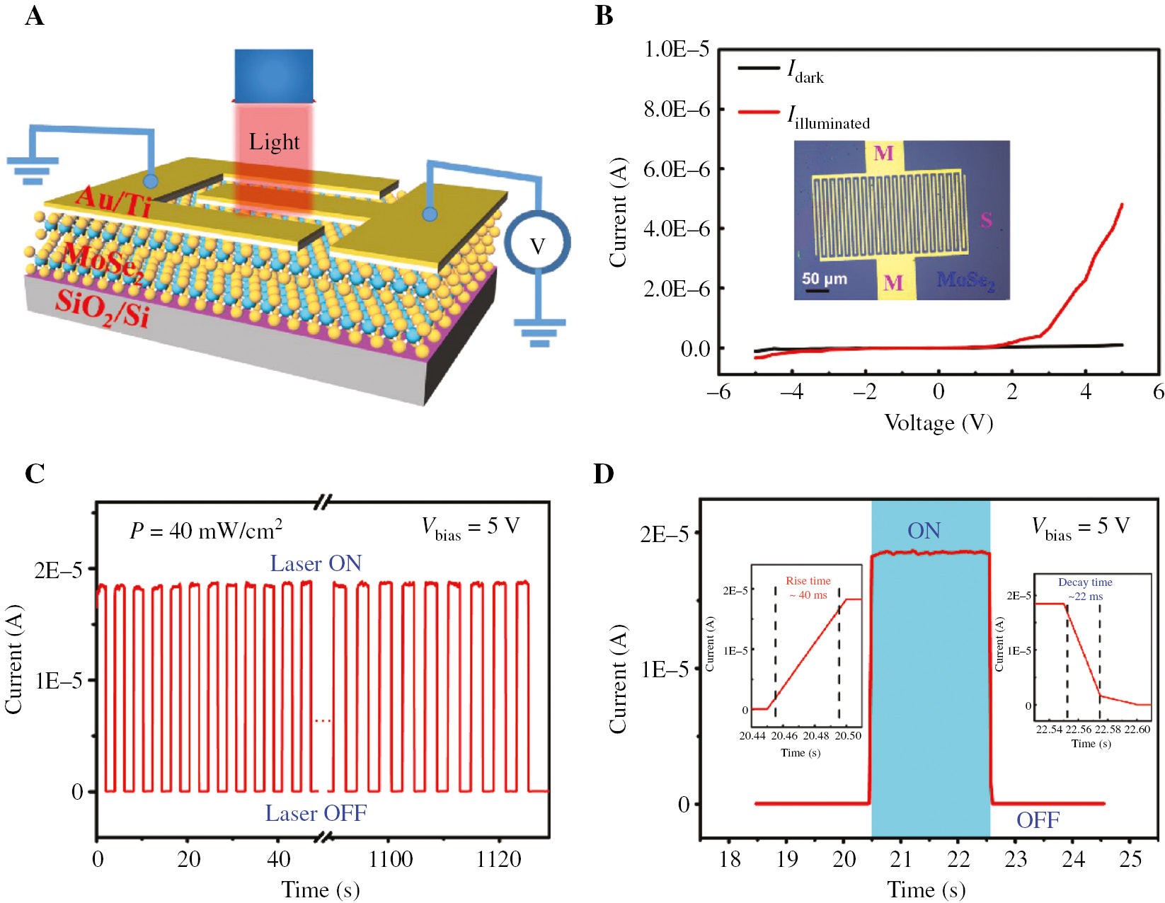
Photoelectrical performance of a few-layer MoSe2.
(A) Schematic representation of MoSe2 MSM PD and a 638 nm laser beam was used for illumination. (B) I-V characteristics in the dark and under light illumination. Inset shows the optical top-view image of a typical device. (C) Stability test of photoswitching behavior of the device at Vbias=5 V and P=40 mW/cm2. (D) Dynamic response characteristics of the PD measured at Vbias=5 V. The corresponding rise and decay process are indicated in the inset.
Figure 5B presents the I-V plots of MoSe2 PD characterized in the dark and under laser illumination with irradiance of 40 mW/cm2 (inset shows a typical device with a contact spacing of 5 μm) and clearly reveals that the current significantly increased as the device on light irradiation is attributed to the increased photogenerated carrier concentration, contributing to the photocurrent Iph (Iph=Iilluminated – Idark). Moreover, the strong nonlinear and asymmetric characteristic addresses the considerable Schottky barrier at the contact. To evaluate the device for potential application, the photoswitching behavior was examined. As indicated in Figure 5C, by continuously switching the light irradiation on/off, reproducible low and high impedance states can be achieved over hundreds of cycles without reduction of the amplitude, displaying a high reversibility and an excellent cycling stability. Additionally, a dark current of 26.8 nA and a photocurrent of up to 18.5 μA give a high light/dark current ratio of 690, allowing the MoSe2-based PD to act as a high-quality photosensitive switch. To explore the original physical mechanisms of the increasing photoconductivity, the schematic energy band diagrams of MoSe2 MSM PD are illustrated in Figure 6C and D. In the dark condition (Figure 6C), the significant surface states resulting from the large surface-to-volume ratios of 2D MoSe2 lower the Schottky barriers at metal/MoSe2 interfaces, facilitating the direct tunneling of electrons (process 1) [42]. Moreover, the polycrystalline nature results in a number of structural defects/disorders that act as trap states, promoting trap-assisted tunneling (process 2) [43], which probably overcome the bandgap-suppressing thermal excitation, generating thermally activated carriers (process 3). Under light irradiation (Figure 6D), photons with energy (wavelength ~638 nm, that is, hν ~1.94 eV) larger than the bandgap of MoSe2 can generate electron-hole pairs, representing the intrinsic transition (process 4), and separated by the external bias voltage to overcome the defect trapping of MoSe2 further overpass the Au:Ti/MoSe2 Schottky barrier, generating the photocurrent. A very fast dynamic response for both rise and decay process is identified in Figure 5D, from which the rise time (from 10% to 90% of the maximum photocurrent) and the decay time (from 90% to 10% of the maximum photocurrent) of MoSe2 MSM PD were estimated to be 40 and 22 ms, respectively. The response time is shorter than the CVD growth single-crystalline MoSe2-based PDs (60–400 ms) [20], [44] and other previously reported MoS2 PD (50 ms) [16]. Such a fast response time presumably due to deep-level defects (effective recombination centers) [45], which give rise to nonradiative (Shockley-Read-Hall type) recombination of nonequilibrium carriers (process 5) [42], [45], [46]. It is noteworthy that the response times could be further improved via increasing the Schottky barrier height between MoSe2 and the contact metal [12].
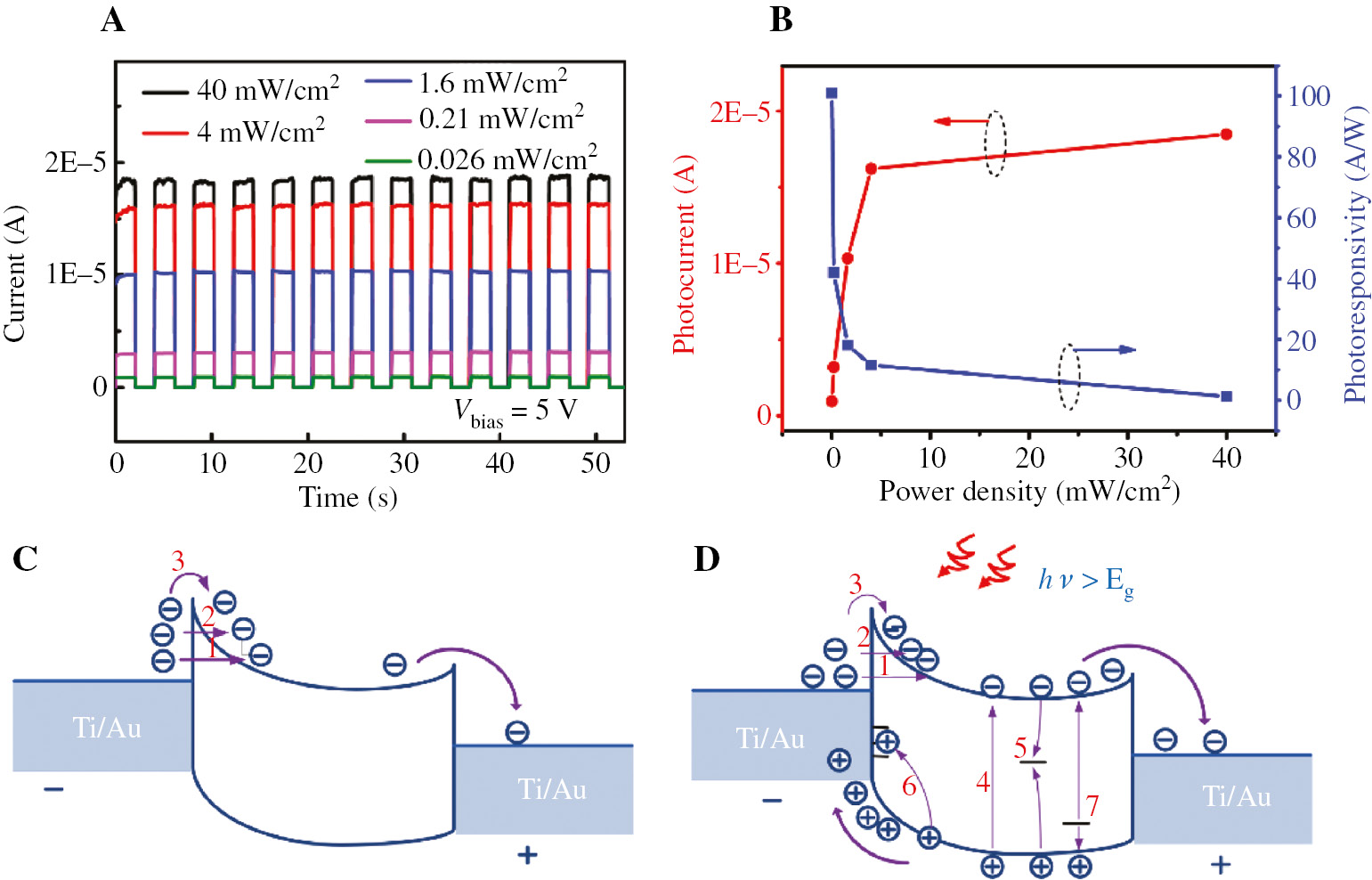
(A) Photocurrent as a function of time with different laser power density modulated. (B) Laser power dependence of the photoresponsivity and photocurrent. Schematic energy band diagrams of the few-layer MoSe2 MSM PD in the dark (C) and under laser illumination (D).
Figure 6A shows the photoresponse modulated by laser illumination with different incident laser power at a bias voltage of 5 V, further confirming the excellent reproducibility and stability of the device, which is important for practical application. Figure 6B (red solid dots line) displays the photocurrent (Iph) as a function of incident light intensity (P), yielding a power-law relationship Iph~P0.43, which shows strong nonlinearity. The obtained index of 0.43 deviates from the ideal factor (~1), meaning that the photoinduced electron-hole pairs in the device involves a complex process including generation, recombination, and trapping [15], [47], [48], further verifying that the inhomogeneous trap distribution in our MoSe2 film originated from the polycrystalline structure. The external photoresponsivity (R) is a critical parameter for a PD, indicating the efficiency of a detector responding to optical signals, which can be calculated as R=Iph/(PS), where P is the light intensity irradiated on the MoSe2 film and S is the effective area under illumination. It was found that the responsivity monotonously decreases with the increase of incident power density as identified in Figure 6B (blue solid squares line), which could be explained by the influence of trap states present in MoSe2 [17] and the enhanced recombination or scattering rate of hot carriers at higher irradiation power [49]. A ultrahigh responsivity of 101 A/W is achieved under incident light intensity of 0.026 mW/cm2 at 5 V bias, which is about 4 orders of magnitude higher than the previously reported PDs based on graphene (6.1 mA/W) [10], SnS2 (8.8 mA/W) [49], and MoS2 (7.5 mA/W) [16] and even substantially higher than that of the highly sensitive PD based on few-layer MoSe2 (97.1 A/W) [14] and MoS2/WSe2 heterojunction (17.8 A/W) [50] (see Table 1 for comparison). We pointed out that the responsivity might be further improved via examining in vacuum/NH3 environment [51], N2H4 treatment [52], laser thinning [53], and surface functionalization [54].
Performance comparison of photodetectors based on a layered 2D nanostructure.a
| Active layer | Vbias (V) | Spectral (nm) | Responsivity | Rise/decay | QE | Detectivity (Jones) | Reference |
|---|---|---|---|---|---|---|---|
| FL-MoSe2-AC | 5 | 638 | 101 A/W | 40/22 ms | 19,668% | 2×10¹³ | This work |
| ML-MoSe2-CVD | 10 | 532 | 13 mA/W | 60/60 ms | – | – | [20] |
| Multi-SnS2-CVD | 2 | 457 | 8.8 mA/W | 5/7 μs | ~2.4% | 2×10⁹ | [49] |
| FL-GaSe-ME | 5 | 254 | 2.8 A/W | 20/37 ms | 1367% | – | [18] |
| FL-GaS-ME | 2 | 254 | 4.2 A/W | <30 ms | 2050% | ~1013–1014 | [19] |
| BL-WS2-CVD | 5 | 457 | 3106 A/W | 59/87 μs | 8.4×10⁵% | 5×10¹² | [21] |
| ML-MoS2-ME | 1 | 550 | 7.5 mA/W | 50 ms | – | – | [16] |
| BL-WS2-CVD | 5 | 532 | 3.5 A/W | – | 933% | 1.6×10¹⁰ | [13] |
| FL-MoSe2-ME | 20 | 532 | 97.1 A/W | 15/30 ms | 22,266% | – | [14] |
| FL-MoS2-TH | 10 | 532 | 0.57 A/W | 70/110 μs | 10% | ~1010 | [12] |
| ML-MoS2-ME | 8 | 561 | 880 A/W | 4/9 s | – | – | [17] |
| Multi-WSe2-PLD | 10 | 635 | 0.92 A/W | 0.9/2 s | 180% | – | [15] |
aAC, ALD and a CVD chamber; FL, few-layer; ME, mechanically exfoliated; ML, monolayer; Multi, multilayer; TH, thermolysis.
EQE represents the number of electron-hole pairs detected per absorbed photon of the incident light and is related to the responsivity. Using the relation
where h is the Planck’s constant, c is the speed of the incident light, e is the elementary charge, and λ denotes the excitation wavelength. The EQE values were evaluated to be as high as 19,668% for MoSe2 PD, which is about 21 times higher than PDs reported for bilayer WS2 with graphene electrodes [13]. It is noteworthy that a larger EQE could be obtained by employing some novel architecture (such as hollow spherical nanoshells and heterojunctions) to improve the light-harvesting efficiency [55], [56]. The extremely high values of R and EQE were primarily ascribed to the photogenerated holes trapped at the Au:Ti/MoSe2 interface, which can (1) reduce the Schottky barrier height due to the light-induced Fermi-level partial pinning effect, producing gain in the photoresponse [57], and (2) induce the sweep-out and reinjection of electrons, leading to the generation of multiple electrons per collected photon (process 6 in Figure 6D) [42]. Moreover, the band tail states in the MoSe2 valence and conduction bands as a result of structural defects/disorders (shallow traps) [42], [45], [46], [58] could contribute to the photoconductive gain (process 7 in Figure 6D). A similar effect has been found in MoS2 PD where the defects in the film were induced by external electrostatic field [59]. In addition, the photogenerated carriers trapped by the adsorbents/water both on the MoSe2 surface and in the MoSe2/SiO2 interface can generate a photogating effect [46], [60], thus leading to a high gain and resulting in a ultrahigh R [60]. Furthermore, specific detectivity (D*) is another important figure of merit for characterizing the sensitivity by taking into account the photoresponse and the noise floor and is defined as D*=(SΔf)1/2/NEP, where Δf is the bandwidth, S is the effective area under illumination, and NEP is the noise equivalent power. Assuming that the total noise of the PD is dominated by the shot noise from dark current, the detectivity can be expressed as
where Id is the dark current [61]. At the low incident power density of 0.026 mW/cm2, our MoSe2 PD exhibits a very high detectivity D* of 2×10¹³ Jones under illumination, which is higher than the commercial Si-based PDs (D*~1012 Jones) [62] as well as InGaAs PDs (D*~1012 Jones). To our knowledge, this value surpasses any of other previously reported MoSe2/MoS2 PDs. It can be attributed to the ultrahigh R and the low Id originates from the Schottky barrier. Accordingly, D* can be further improved by increasing the responsivity and reducing the dark current [12], [63]. Particularly, D* could be enhanced by introducing plasmonic nanoparticles on the surface of MoSe2 film [64]. Additionally, the critical device metrics of the proposed MoSe2 PD have been compared to those of other reported 2D nanosheet devices (as listed in Table 1), demonstrating that the synthesized few-layer MoSe2 films are promising for highly sensitive PDs. Hence, compared to the perfect single-crystalline 2D MoSe2, we incline to suggest employing polycrystalline films with some traps/structure defects for high-performance PD applications.
4 Conclusion
To summarize, we successfully synthesized 2H-MoSe2 few-layer films on SiO2 substrates with wafer-level homogeneous and continuous via ALD and a CVD method. Subsequently, an MSM PD based on the few-layer MoSe2 film was fabricated. The photoconductivity mechanisms in the atomically thin MoSe2 film were discussed in depth based on the analysis of the material properties. Impressively, the excellent figures of merits such as response time, EQE, responsivity, and specific detectivity of MoSe2-based PD are 22 ms, 19,668%, 101A/W, and 2×10¹³ Jones, respectively, substantially superior to their counterparts based on CVD-grown or mechanically exfoliated single-crystalline MoSe2 as well as higher than those reported in other few-layer semiconductors, such as WS2, MoS2, WSe2, GaSe, GaS, and SnS2. Especially, the ultrahigh D* was not obtainable in 2D MoSe2/MoS2 and many of other TMD PDs previously. We believe that this work opens an avenue for the large-scale production of high-performance MoSe2 PDs and lays the foundation for their future applications in integrated optoelectronic systems.
Acknowledgments
The work was supported by the National Nature Science Foundation of China under contracts 51572043 and 61875029.
References
[1] Wang JX, Sun XW, Yang Y, et al. Hydrothermally grown oriented ZnO nanorod arrays for gas sensing applications. Nanotechnology 2006;17:4995–8.10.1088/0957-4484/17/19/037Suche in Google Scholar
[2] Konstantatos G, Howard I, Fischer A, et al. Ultrasensitive solution-cast quantum dot photodetectors. Nature 2006;442:180–3.10.1038/nature04855Suche in Google Scholar PubMed
[3] Li L, Fang X, Zhai T, et al. Electrical transport and high-performance photoconductivity in individual ZrS2 nanobelts. Adv Mater 2010;22:4151–6.10.1002/adma.201001413Suche in Google Scholar PubMed
[4] Li L, Wu P, Fang X, et al. Single-crystalline CdS nanobelts for excellent field-emitters and ultrahigh quantum-efficiency photodetectors. Adv Mater 2010;22:3161–5.10.1002/adma.201000144Suche in Google Scholar PubMed
[5] Soci C, Zhang A, Xiang B, et al. ZnO nanowire UV photodetectors with high internal gain. Nano Lett 2007;7:1003–9.10.1021/nl070111xSuche in Google Scholar PubMed
[6] Xia F, Mueller T, Lin Y-m, Valdes-Garcia A, Avouris P. Ultrafast graphene photodetector. Nat Nanotechnol 2009;4:839–43.10.1038/nnano.2009.292Suche in Google Scholar PubMed
[7] Bonaccorso F, Sun Z, Hasan T, Ferrari AC. Graphene photonics and optoelectronics. Nat Photon 2010;4:611–22.10.1038/nphoton.2010.186Suche in Google Scholar
[8] Koppens FHL, Mueller T, Avouris P, Ferrari AC, Vitiello MS, Polini M. Photodetectors based on graphene, other two-dimensional materials and hybrid systems. Nat Nanotechnol 2014;9:780–93.10.1038/nnano.2014.215Suche in Google Scholar PubMed
[9] Nair RR, Blake P, Grigorenko AN, et al. Fine structure constant defines visual transparency of graphene. Science 2008;320:1308.10.1126/science.1156965Suche in Google Scholar PubMed
[10] Mueller T, Xia F, Avouris P. Graphene photodetectors for high-speed optical communications. Nat Photon 2010;4:297–301.10.1038/nphoton.2010.40Suche in Google Scholar
[11] Zhang TF, Wu GA, Wang JZ, et al. A sensitive ultraviolet light photodiode based on graphene-on-zinc oxide Schottky junction. Nanophotonics 2017;6:1073–81.10.1515/nanoph-2016-0143Suche in Google Scholar
[12] Tsai DS, Liu KK, Lien DH, et al. Few-layer MoS2 with high broadband photogain and fast optical switching for use in harsh environments. ACS Nano 2013;7:3905–11.10.1021/nn305301bSuche in Google Scholar PubMed
[13] Tan H, Fan Y, Zhou Y, Chen Q, Xu W, Warner JH. Ultrathin 2D photodetectors utilizing chemical vapor deposition grown WS2 with graphene electrodes. ACS Nano 2016;10:7866–73.10.1021/acsnano.6b03722Suche in Google Scholar PubMed
[14] Abderrahmane A, Ko PJ, Thu TV, Ishizawa S, Takamura T, Sandhu A. High photosensitivity few-layered MoSe2 back-gated field-effect phototransistors. Nanotechnology 2014;25:365202.10.1088/0957-4484/25/36/365202Suche in Google Scholar PubMed
[15] Zheng Z, Zhang T, Yao J, Zhang Y, Xu J, Yang G. Flexible, transparent and ultra-broadband photodetector based on large-area WSe2 film for wearable devices. Nanotechnology 2016;27:225501.10.1088/0957-4484/27/22/225501Suche in Google Scholar PubMed
[16] Yin Z, Li H, Li H, et al. Single-layer MoS2 phototransistors. ACS Nano 2012;6:74–80.10.1021/nn2024557Suche in Google Scholar PubMed
[17] Lopez-Sanchez O, Lembke D, Kayci M, Radenovic A, Kis A. Ultrasensitive photodetectors based on monolayer MoS2. Nat Nanotechnol 2013;8:497–501.10.1038/nnano.2013.100Suche in Google Scholar PubMed
[18] Hu P, Wen Z, Wang L, Tan P, Xiao K. Synthesis of few-layer GaSe nanosheets for high performance photodetectors. ACS Nano 2012;6:5988–94.10.1021/nn300889cSuche in Google Scholar PubMed
[19] Hu P, Wang L, Yoon M, et al. Highly responsive ultrathin GaS nanosheet photodetectors on rigid and flexible substrates. Nano Lett 2013;13:1649–54.10.1021/nl400107kSuche in Google Scholar PubMed
[20] Xia J, Huang X, Liu LZ, et al. CVD synthesis of large-area, highly crystalline MoSe2 atomic layers on diverse substrates and application to photodetectors. Nanoscale 2014;6:8949–55.10.1039/C4NR02311KSuche in Google Scholar PubMed
[21] Yang R, Feng S, Xiang J, et al. Ultrahigh-gain and fast photodetectors built on atomically thin bilayer tungsten disulfide grown by chemical vapor deposition. ACS Appl Mater Interfaces 2017;9:42001–10.10.1021/acsami.7b14853Suche in Google Scholar PubMed
[22] Ling ZP, Yang R, Chai JW, et al. Large-scale two-dimensional MoS2 photodetectors by magnetron sputtering. Opt Express 2015;23:13580–6.10.1364/OE.23.013580Suche in Google Scholar PubMed
[23] Chang YH, Zhang W, Zhu Y, et al. Monolayer MoSe2 grown by chemical vapor deposition for fast photodetection. ACS Nano 2014;8:8582–90.10.1021/nn503287mSuche in Google Scholar PubMed
[24] Buscema M, Island JO, Groenendijk DJ, et al. Photocurrent generation with two-dimensional van der Waals semiconductors. Chem Soc Rev 2015;44:3691–718.10.1039/C5CS00106DSuche in Google Scholar PubMed
[25] Mao J, Yu Y, Wang L, et al. Ultrafast, broadband photodetector based on MoSe2/silicon heterojunction with vertically standing layered structure using graphene as transparent electrode. Adv Sci 2016;3:1600018.10.1002/advs.201600018Suche in Google Scholar PubMed PubMed Central
[26] Jiang M, Zhang J, Wu M, et al. Synthesis of 1T-MoSe2 ultrathin nanosheets with an expanded interlayer spacing of 1.17 nm for efficient hydrogen evolution reaction. J Mater Chem A 2016;4:14949–53.10.1039/C6TA07020ESuche in Google Scholar
[27] Chhowalla M, Shin HS, Eda G, Li LJ, Loh KP, Zhang H. The chemistry of two-dimensional layered transition metal dichalcogenide nanosheets. Nat Chem 2013;5:263–75.10.1038/nchem.1589Suche in Google Scholar PubMed
[28] Dai T, Ren Y, Qian L, Liu X. Characterization of molybdenum oxide thin films grown by atomic layer deposition. J Electron Mater 2018;47:6709–15.10.1007/s11664-018-6555-4Suche in Google Scholar
[29] Lu X, Utama MI, Lin J, et al. Large-area synthesis of monolayer and few-layer MoSe2 films on SiO2 substrates. Nano Lett 2014;14:2419–25.10.1021/nl5000906Suche in Google Scholar PubMed
[30] Huang JK, Pu J, Hsu CL, et al. Large-area synthesis of highly crystalline WSe2 monolayers and device applications. ACS Nano 2014;8:923–30.10.1021/nn405719xSuche in Google Scholar PubMed
[31] Shim GW, Yoo K, Seo SB, et al. Large-area single-layer MoSe2 and its van der Waals heterostructures. ACS Nano 2014;8:6655–62.10.1021/nn405685jSuche in Google Scholar PubMed
[32] Blackburn PE, Hoch M, Johnston HL. The vaporization of molybdenum and tungsten oxides. J Phys Chem 1958;62:769–73.10.1021/j150565a001Suche in Google Scholar
[33] Bradley AJ, Ugeda MM, Jornada FHD, et al. Probing the role of interlayer coupling and Coulomb interactions on electronic structure in few-layer MoSe2 nanostructures. Nano Lett 2015;15:2594–9.10.1021/acs.nanolett.5b00160Suche in Google Scholar PubMed PubMed Central
[34] Wang X, Gong Y, Shi G, et al. Chemical vapor deposition growth of crystalline monolayer MoSe2. ACS Nano 2014;8:5125–31.10.1021/nn501175kSuche in Google Scholar PubMed
[35] Song JG, Park J, Lee W, et al. Layer-controlled, wafer-scale, and conformal synthesis of tungsten disulfide nanosheets using atomic layer deposition. ACS Nano 2013;7:11333–40.10.1021/nn405194eSuche in Google Scholar PubMed
[36] Lin YC, Zhang W, Huang JK, et al. Wafer-scale MoS2 thin layers prepared by MoO3 sulfurization. Nanoscale 2012;4:6637–41.10.1039/c2nr31833dSuche in Google Scholar PubMed
[37] Ding Y, Wang Y, Ni J, Shi L, Shi S, Tang W. First principles study of structural, vibrational and electronic properties of graphene-like MX2 (M=Mo, Nb, W, Ta; X=S, Se,Te) monolayers. Physica B 2011;406:2254–60.10.1016/j.physb.2011.03.044Suche in Google Scholar
[38] O’Brien M, McEvoy N, Hanlon D, Hallam T, Coleman JN, Duesberg GS. Mapping of low-frequency Raman modes in CVD-grown transition metal dichalcogenides: layer number, stacking orientation and resonant effects. Sci Rep 2016;6:19476.10.1038/srep19476Suche in Google Scholar PubMed PubMed Central
[39] Tongay S, Zhou J, Ataca C, et al. Thermally driven crossover from indirect toward direct bandgap in 2D semiconductors: MoSe2 versus MoS2. Nano Lett 2012;12:5576–80.10.1021/nl302584wSuche in Google Scholar PubMed
[40] Tonndorf P, Schmidt R, Böttger P, et al. Photoluminescence emission and Raman response of monolayer MoS2, MoSe2, and WSe2. Opt Express 2013;21:4908–16.10.1364/OE.21.004908Suche in Google Scholar PubMed
[41] Diskus M, Nilsen O, Fjellvåg H. Growth of thin films of molybdenum oxide by atomic layer deposition. J Mater Chem 2011;21:705–10.10.1039/C0JM01099ESuche in Google Scholar
[42] Qian LX, Wu ZH, Zhang YY, Lai PT, Liu XZ, Li YR. Ultrahigh-responsivity, rapid-recovery, solar-blind photodetector based on highly nonstoichiometric amorphous gallium oxide. ACS Photonics 2017;4:2203–11.10.1021/acsphotonics.7b00359Suche in Google Scholar
[43] Heinemann MD, Berry J, Teeter G, Unold T, Ginley D. Oxygen deficiency and Sn doping of amorphous Ga2O3. Appl Phys Lett 2016;108:022107.10.1063/1.4938473Suche in Google Scholar
[44] Jung C, Kim SM, Moon H, et al. Highly crystalline CVD-grown multilayer MoSe2 thin film transistor for fast photodetector. Sci Rep 2015;5:15313.10.1038/srep15313Suche in Google Scholar PubMed PubMed Central
[45] Zhu W, Low T, Lee YH, et al. Electronic transport and device prospects of monolayer molybdenum disulphide grown by chemical vapour deposition. Nat Commun 2014;5:3087.10.1038/ncomms4087Suche in Google Scholar PubMed
[46] Furchi MM, Polyushkin DK, Pospischil A, Mueller T. Mechanisms of photoconductivity in atomically thin MoS2. Nano Lett 2014;14:6165–70.10.1021/nl502339qSuche in Google Scholar PubMed
[47] Liu G, Li Z, Chen X, et al. Non-planar vertical photodetectors based on free-standing two-dimensional SnS2 nanosheets. Nanoscale 2017;9:9167–74.10.1039/C7NR03646ASuche in Google Scholar PubMed
[48] Hafeez M, Gan L, Li H, Ma Y, Zhai T. Chemical vapor deposition synthesis of ultrathin hexagonal ReSe2 flakes for anisotropic Raman property and optoelectronic application. Adv Mater 2016;28:8296–301.10.1002/adma.201601977Suche in Google Scholar PubMed
[49] Su G, Hadjiev VG, Loya PE, et al. Chemical vapor deposition of thin crystals of layered semiconductor SnS2 for fast photodetection application. Nano Lett 2015;15:506–13.10.1021/nl503857rSuche in Google Scholar PubMed
[50] Sun M, Fang Q, Xie D, et al. Novel transfer behaviors in 2D MoS2/WSe2 heterotransistor and its applications in visible-near infrared photodetection. Adv Electron Mater 2017;3:1600502.10.1002/aelm.201600502Suche in Google Scholar
[51] Huo N, Yang S, Wei Z, Li SS, Xia JB, Li J. Photoresponsive and gas sensing field-effect transistors based on multilayer WS2 nanoflakes. Sci Rep 2014;4:5209.10.1038/srep05209Suche in Google Scholar PubMed PubMed Central
[52] Sun M, Xie D, Sun Y, Li W, Ren T. Locally hydrazine doped WSe2 p-n junction toward high-performance photodetectors. Nanotechnology 2018;29:015203.10.1088/1361-6528/aa96e9Suche in Google Scholar PubMed
[53] Lu J, Lu JH, Liu H, et al. Improved photoelectrical properties of MoS2 films after laser micromachining. ACS Nano 2014;8:6334–43.10.1021/nn501821zSuche in Google Scholar PubMed
[54] Kang DH, Kim MS, Shim J, et al. High-performance transition metal dichalcogenide photodetectors enhanced by self-assembled monolayer doping. Adv Funct Mater 2015;25:4219–27.10.1002/adfm.201501170Suche in Google Scholar
[55] Chen X, Yang HY, Liu G, et al. Hollow spherical nanoshell arrays of 2D layered semiconductor for high-performance photodetector device. Adv Funct Mater 2018;28:1705153.10.1002/adfm.201705153Suche in Google Scholar
[56] Chen X, Qiu Y, Yang H, et al. In-plane mosaic potential growth of large-area 2D layered semiconductors MoS2-MoSe2 lateral heterostructures and photodetector application. ACS Appl Mater Interfaces 2017;9:1684–91.10.1021/acsami.6b13379Suche in Google Scholar PubMed
[57] Katz O, Garber V, Meyler B, Bahir G, Salzman J. Gain mechanism in GaN Schottky ultraviolet detectors. Appl Phys Lett 2001;79:1417–9.10.1063/1.1394717Suche in Google Scholar
[58] Ghatak S, Ghosh A. Observation of trap-assisted space charge limited conductivity in short channel MoS2 transistor. Appl Phys Lett 2013;103:122103.10.1063/1.4821185Suche in Google Scholar
[59] Wang X, Wang P, Wang J, et al. Ultrasensitive and broadband MoS2 photodetector driven by ferroelectrics. Adv Mater 2015;27:6575–81.10.1002/adma.201503340Suche in Google Scholar PubMed
[60] Fang H, Hu W. Photogating in low dimensional photodetectors. Adv Sci 2017;4:1700323.10.1002/advs.201700323Suche in Google Scholar PubMed PubMed Central
[61] Xie C, Mak C, Tao X, Yan F. Photodetectors based on two-dimensional layered materials beyond graphene. Adv Funct Mater 2017;27:1603886.10.1002/adfm.201603886Suche in Google Scholar
[62] Wegrzecka I, Wegrzecki M, Grynglas M, et al. Design and properties of silicon avalanche photodiodes. Opto-Electron Rev 2004;12:95–104.Suche in Google Scholar
[63] Sun M, Fang Q, Xie D, et al. Heterostructured graphene quantum dot/WSe2/Si photodetector with suppressed dark current and improved detectivity. Nano Res 2018;11:3233–43.10.1007/s12274-017-1855-1Suche in Google Scholar
[64] Dai M, Chen H, Feng R, et al. A dual-band multilayer InSe self-powered photodetector with high performance induced by surface plasmon resonance and asymmetric Schottky junction. ACS Nano 2018;12:8739–47.10.1021/acsnano.8b04931Suche in Google Scholar PubMed
Supplementary Material
The online version of this article offers supplementary material (https://doi.org/10.1515/nanoph-2018-0153).
©2018 Xing-Zhao Liu, Dan Xie et al., published by De Gruyter, Berlin/Boston
This work is licensed under the Creative Commons Attribution-NonCommercial-NoDerivatives 4.0 License.
Artikel in diesem Heft
- Review Articles
- High-efficiency broadband light coupling between optical fibers and photonic integrated circuits
- Plasmonic particle-on-film nanocavities: a versatile platform for plasmon-enhanced spectroscopy and photochemistry
- Coupling configurations between extended surface electromagnetic waves and localized surface plasmons for ultrahigh field enhancement
- Research Articles
- Laser-induced thermoelectric effects in electrically biased nanoscale constrictions
- Photonic spin Hall effect of monolayer black phosphorus in the Terahertz region
- On-chip optical parity checker using silicon photonic integrated circuits
- Stretchable and self-healable organometal halide perovskite nanocrystal-embedded polymer gels with enhanced luminescence stability
- Synthesis of few-layer 2H-MoSe2 thin films with wafer-level homogeneity for high-performance photodetector
- Aberration correction for improving the image quality in STED microscopy using the genetic algorithm
- Electroluminescence and photo-response of inorganic halide perovskite bi-functional diodes