
Laser-induced thermoelectric effects in electrically biased nanoscale constrictions
-
Marie-Maxime Mennemanteuil


Abstract
Electrically biased metal nanostructures are at the core of innovative multifunctional integrated devices that control the flow of electrons and photons at the nanoscale. They are based on plasmonic structures that create strongly confined fields, typically associated with large temperature gradients. These thermal effects may generate artifact responses detrimental to the desired operation. We show here how a biasing polarity and a local optical excitation asymmetry of a generic geometry – a nanoscale constriction – interplay thermally to modify the diffusive electron transport in out-of-equilibrium conditions. Our experimental results are accompanied with computational electromagnetism and multiphysics simulations.
1 Introduction
The transduction of electrons and photons at the nanoscale is a key functionality to develop the next generation of integrated energy-friendly optoelectronic devices operating at high speeds. Thus, there has been an increase in the portfolio of functional metal-based devices enabling advanced operations while maintaining strong light confinement. For instance, coplanar electrically contacted atomic-scale gaps allow a variety of functions embedded with the same architecture: they can be operated as optical antennas emitting radiation upon the injection of charge carriers [1], [2], [3], [4], as photodetectors producing direct current (d.c.) by optical rectification [5], [6], [7], or integrated as controlled plasmonic switches [8]. A combination of these functionalities in a single platform has been recently reported for the on-chip excitation and detection of surface plasmon polaritons [9] or for transducing optical power transferred wirelessly at the microscale [10]. Moreover, light-harvesting plasmonic systems based on the collection of hot carriers also benefit from these new optoelectronic components [11], [12], [13].
In these few examples, heat generation and thermal gradients due to light absorption may jeopardize the optimum performance of the device or hide the physical origin responsible for the flow of charge. An increase of temperature leads to thermal expansion, which is particularly adverse for atomic-sized gaps [14]. The light-induced heat gradients within the device inevitably lead to thermovoltages and thermocurrents [15], [16], [17] with time responses orders of magnitude slower than those associated with current produced by, for example, optical rectification. These asymmetries of the temperature profile are generally neglected in describing the operation of devices collecting hot electrons. However, a precise manipulation of the temperature and the flow of heat is possible with optimized structures [18], [19]. For instance, the generation of currents due to laser-induced thermoelectrical effects may function as driven switches [20]. To understand current-carrying devices, we must distinguish contributions stemming from optically induced processes from those having a thermal origin [21].
In this contribution, we report a case study where electronic transport in the nanostructure obeys the laws of thermoelectricity and its associated effects, especially the Seebeck mechanism. We perturb an electrically biased nanoscale bowtie-like constriction with a local laser excitation. A nanoscale constriction is interesting because, when flanked by triangular reservoirs, the structure concentrates incoming electromagnetic field and maximizes the temperature gradient and the expected thermoelectrical conversion [22]. Furthermore, when electrons pass through a biased constriction, they may transfer their energy to an electromagnetic field very efficiently [23]. Finally, nanoscale constrictions are also the starting geometry for realizing atomic-scale feedgaps in emissive optical antennas and rectennas [1], [4], [6], [7].
In the following, upon locally exciting the bowtie with a focused laser beam, we measure a zero-bias thermocurrent circulating in the constriction. We register both the amplitude and direction of these currents. They both depend on the precise nanometric positioning of the laser spot, confirming the results reported in a recent contribution [17]. We further investigate how light-induced thermal transport is affected when the constriction is biased, that is, when a current flow and a heat flow exist simultaneously in the device. Our experimental data are accurately reproduced through a three-dimensional finite element analysis.
2 Fabrication and measurement protocols
The constriction and the electrical connections are produced through a double-step lithography. First, we realize the constriction and the proximity electrodes by electron-beam lithography (Pioneer, Raith GmbH) on an electron-sensitive resist spin coated on a glass coverslip (Agar, No. 1). After development, we evaporate a 2-nm-thick adhesion layer of Cr and a 50-nm-thick Au film. This step is finalized by a lift-off procedure. In the second step, an optical lithography (MJB4, Süss Microtech., GmbH) creates the macroscopic electrodes connecting the constrictions to the external instrumentation. The electrodes are also produced by evaporation of Cr and Au layers. Figure 1A shows a scanning electron microscopy (SEM) image of one of our constrictions. The width of the constriction is 100 nm, which is formed at the contact point between the two proximity triangular electrodes. The transport regime in this size range remains diffusive.
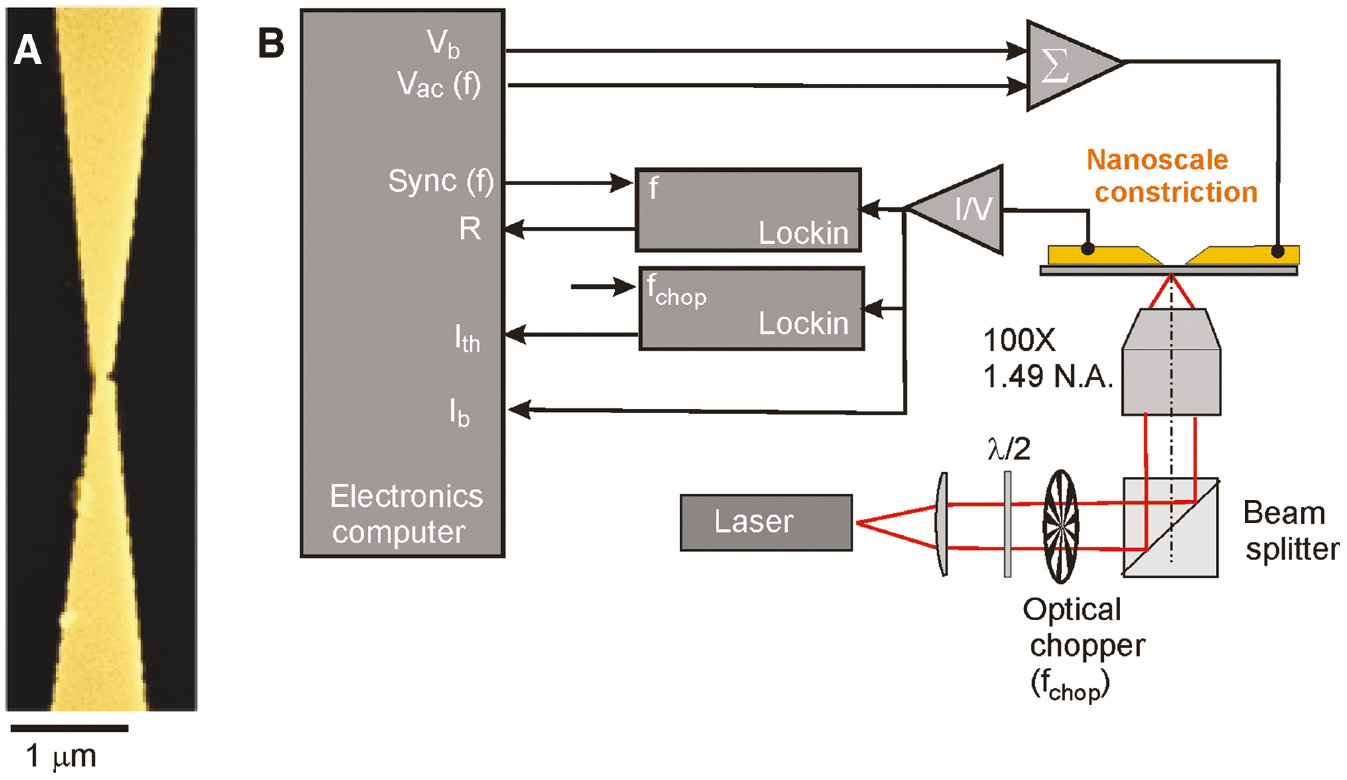
Gold constriction and experimental setup.
(A) Colored SEM image of a typical nanoscale Au constriction fabricated on a glass substrate. The narrowest width is 100 nm and the yellow hue corresponds to the Au material. (B) Schematic representation of the setup used for optical excitation and electrical addressing. The total voltage applied to the constriction is the addition of a static bias Vb and a 20 mV sinusoidal voltage Vac oscillating at the frequency f=12.6 kHz. The laser is periodically chopped at fchop=831 Hz. A lock-in detection extracts the different frequency contributions to the total current measured by a current-to-voltage converter (I/V).
Figure 1B depicts the schematic of the experimental setup with the laser excitation, electrical connections, and signal read-out. We excite the device with a laser emitting at 785 nm tightly focused from the backside of the glass substrate by a high numerical aperture oil immersion objective (N.A.=1.49; ×100) of an inverted optical microscope (Eclipse Ti-E, Nikon). A half-wave plate controls the polarization of the incident beam, and the laser is mechanically chopped at a frequency fchop=831 Hz to avoid harmonics of the ac power line and to integrate enough measurement cycles during the dwell time per pixel when raster scanning the sample through the focus. The results shown below do not depend on the range of frequencies accessible by the laser chopper. The sample sits on a two-dimensional linearized piezoelectric stage (Nano LP100, Mad City Labs) controlling the in-plane (x, y) position of the sample within the focal plane. The electrical bias Vb is provided by a stabilized voltage source (SPM100, RHK Technology). When needed, a small alternative voltage Vac=20 mV is added to Vb such that the total voltage is Vb + Vaccos(ωt), where ω=2πf is the angular frequency of the alternating voltage with f=12.6 kHz. We measure the total current flowing through the system Ib with a current-to-voltage amplifier (I/V) placed at the ground electrode and with an adjustable gain (DLPCA, Femto GmbH). Using a first lock-in detection (UHLI, Zurich Instruments) synced at fchop, we extract the laser-induced contribution from the total current. With the help of a second lock-in detection referenced at f, we monitor the resistance R of the constriction [6]. The measurement synced to the modulation frequency of the bias voltage averages the results of the “on” and “off” states of the laser irradiance. The I/V converter and lock-in outputs are fed into a scanning probe electronics (SPM 100, RHK Technology) to reconstruct pixel-by-pixel images of the different signals as a function of the (x, y) position of the laser spot with respect to the sample.
3 Modeling and simulation framework
For the sake of simplicity and clarity, the physical model used in this contribution remains classical and we have not taken into account any quantum effect. The minimum sizes (50×100 nm2 at the neck of the constriction) are large enough to behave classically in both the electromagnetic and thermal domains. The laser beam is considered monochromatic, polarized along the direction of the axis of symmetry of the structure. It is focused on the plane of the device and has a lateral Gaussian shape. Although the experimental irradiance distribution slightly departs from the Gaussian profile, we checked that a top-hat distribution having the same size than the Gaussian one, provides very similar results when moving the calculations to the thermal domain to evaluate the thermocurrents. Under these conditions, we numerically compute the absorbed power in the device under test. As reported recently by Zolotavin et al. [17], the absorption of the laser by the metal structure acts as a local source of heat, creating an inhomogeneous temperature distribution in the system. The deposited power is modeled as a cylindrical heat source Q, appearing in the heat transfer equation:
where ρm is the mass density, Cp is the heat capacity at constant pressure, k is the thermal conductivity, and T is the temperature. Heat transfer works quite efficiently at the nanoscale and allows for a stationary treatment [18]. We therefore neglect the time-varying term on the left side of Eq. (1). The flow of power generates a temperature map that is numerically calculated in the stationary state through a finite element approach using the commercial software COMSOL. We denote the position of the laser spot as (x, y), whereas the local coordinates on the sample is referred as (u, v) for any location of the laser spot. After solving the heat transfer equation, we obtain a detailed map of the temperature distribution Tlocal(u, v) for a given position of the laser (x, y).
Once the temperature map is obtained, we include the thermoelectric effects. Each position (x, y) of the laser spot generates a different temperature distribution Tlocal(u, v), producing a thermocurrent density Jth(u, v), locally distributed as
where σ and S are the electric conductivity and Seebeck coefficient of the metal respectively, and Tlocal(u, v) is the local temperature distribution in the geometry for the given location (x, y) of the laser. After adding up the individual contributions of each point of the structure Jth(u, v), the thermoelectric intensity is calculated by integrating over the section of the device.
When biasing is present, all those charge carriers set in motion by the laser-induced thermocurrent are now drifted by the bias. This additional term in the thermocurrent can be written as
where kB is the Boltzmann constant and e is the electron charge. Imax denotes the maximum value reached by the current. It accounts for all the charge carriers set in motion when the laser heats the structure and the bias is applied. The term
4 Thermocurrent at Vb=0 V
We consider a nonbiased constriction irradiated by a focused laser with an intensity of about 500 kW cm−2. The sample is raster scanned laterally under the focused laser spot, and the output of the I/V converter is recorded for each position. The linear polarization of the laser is oriented along the main axis of the constriction.
The rise in temperature is driven by the absorption cross-section of the geometry and by heat dissipation mechanisms. The thermal load is mitigated because the metal is in direct contact with the substrate, where heat is exchanged efficiently [5], [24]. From previous reports obtained with the help of bolometric measurements, the temperature was shown to typically increase by a few degrees [16], [24], [25]. In our case, the temperature variation is also inferred by a combination of computational analysis of the problem and bolometric measurements. We obtain a detailed map of the temperature distribution Tlocal(u, v) along with the value of the maximum temperature Tmax and the averaged one TA(x, y) from a three-dimensional finite analysis of the experimental geometry. Figure 2A shows the calculated local temperature distributions as ΔTlocal(u, v)=Tlocal(u, v) – T0 computed for three different laser positions (green circles) along the axis of the constriction and for two values of the bias voltage, Vb=0 mV and Vb=+24 mV (this non-zero biasing result will be discussed later). T0=293.15 K is the room temperature and it is also used in the thermal domain calculation as a contour condition. The laser spot has a diameter of 350 nm, a value comparable to the experimental diffraction-limited focus. The profiles on the left of Figure 2A are obtained along the vertical axis of the constriction for two values of Vb in red and blue. The constant dotted line represents the average of temperature along this profile for the given locations of the laser spot and bias voltages. As expected, the maximum local and average temperatures are obtained when the laser overlaps and fills the metal constriction near the neck of the structure. When moving from this position, the temperature (both maximum and averaged) decreases. If the laser overfills the metal, the deposited energy essentially dissipates via an exchange with the substrate. However, if the beam underfills the metal, the greater thermal conductivity of the metal distributes the thermal load over a larger area and temperature decreases.

Computed and measured temperature maps.
(A) Temperature profiles and maps, ΔTlocal(u, v), calculated for three positions of the laser spot (green circles). The profiles show the temperature distributions along the axis of the constriction. The thin red line in the profiles corresponds to Vb=0 mV, and the thick blue line correspond to Vb=24 mV. The dotted lines represent the average of these profiles, ΔTA, which are related to the global temperature ΔTG. (B) Reconstructed confocal map of the variation of the constriction resistance ΔR(x, y) when the constriction is scanned pixel by pixel under the laser spot. The color bar on the right of the map represents the global temperature change, ΔTG(x, y), where the spatial dependence is linked to the location of the laser spot. Resistance variation and temperature are proportional to each other and can be represented with the same color map. This linear relation is given by the calibration curve at the right plot of (B). The linear fitting follows the relation ΔR=0.03ΔTG. (C) Profile of ΔR(x, y) along the y axis with an average of five pixels around the symmetry axis. The black thick line is the mean of these values and the gray thin ones around it are one standard deviation apart. The red circles represent the simulated results, and the error bars account for a 10% variation of the geometrical parameters of the structure and the incidence laser irradiance.
Figure 2B shows an experimental confocal map of the relative variation of the constriction resistance ΔR(x, y)=Ron(x, y) – Roff when scanning the sample through the focus. We measure resistances Ron(x, y) and Roff via lock-in detection of the current with an alternating bias Vaccos(ωt) applied to the sample and when the laser is periodically chopped “on” and “off”. The temperature rise of the metal provoked by light absorption leads to an increase of ΔR(x, y). The resistance of the constriction deduced from a four-probe analysis removing the contribution of the electrical contacts is Rconstr=14 Ω. We also show in Figure 2B the calibration curve relating the variation of the resistance with the global temperature of the sample. To obtain this relation, the temperature was varied by placing the entire sample on a controllable Peltier plate. For this constriction, an elevation of 1 K changes the resistance by ΔR=0.03 Ω. This calibration provides an estimate of the average global temperature variation ΔTG of the structure (see the color bar of the map in Figure 2B).
To compare the results given by our thermal simulations (Figure 2A) to the measured changes in resistance (Figure 2B), we have plotted in Figure 2C the experimental profile of ΔR obtained along the axis of the constriction. This is represented by a thick black solid line taken as the average of five columns around this axis. The thin gray lines represent the limits given by one standard deviation of the same five columns around the axis. The values of ΔTG presented on the right axis of this figure are obtained after applying the calibration factor shown in Figure 2B. We transform the simulated temperature distributions to resistance variations for each location of the spot through a bolometric model using the temperature coefficient of resistance value (α):
where the integral is evaluated along the trajectory L over the v axis. The integration describes the in-series combination of the resistance at each location of the structure along the v axis. ΔTlocal(v) is the profile in local temperature along the v axis obtained from ΔTlocal(u, v) maps. The resistance for a portion dv is dR=ρdv([w(v)h], where ρ and h are the electric resistivity and the thickness of the metal, respectively, and w(v) is the width of the structure following the constriction geometry. This width is w(v)=w0+2vtan(ϕ/2), where w0 is the neck width and ϕ is the total flare angle of the structure. This evaluation has been repeated allowing a 10% variation of the geometrical parameters of the constriction (thickness h, neck width w0, and flare angle ϕ) and the delivered power to the sample. The motivation behind exploring this range of variations is essentially to evaluate the sensibility of ΔR (and ΔT) when some of the geometrical parameters are changed. Although electron beam lithography is a precise manufacturing tool, a conservative approach is to consider 25 nm as a reasonable uncertainty value for the lateral dimensions of the devices. The error bars in Figure 2C represent this variation. The central red circles correspond to the calculation when the nominal designed values are considered. These values are ω0=100 nm, h=50 nm, and ϕ=15°. In these calculations, the resistivity of gold is adjusted to fit the measured value of the resistance of the constriction (14 Ω) with the total resistance of the modeled geometry using nominal values. The resistivity value is about 1.5 times larger than the bulk resistivity of gold ρAu=2.4×10⁻⁸ Ωm. This value is in accordance with previous reported results extracted from thin films [26], [27].
Summarizing these findings, we may see that the plots and maps in Figure 2 combine three variations in temperature. ΔTlocal is represented in Figure 2A as maps and longitudinal profiles. ΔTA is evaluated from these profiles. Both ΔTlocal and ΔTA are obtained numerically. ΔTG appears first in Figure 2B after converting ΔR measurements in temperature variations. The map of ΔR in Figure 2B is used in Figure 2C to compare it to the calculated resistance variation obtained through a bolometric model using the profile of ΔTlocal along the axis of the structure. Equation (4), which considers the temperature and geometry profiles, enhances the contribution of the middle of the structure. This approach provides a value of ΔR larger than the one obtainable when considering a constant value for the temperature along the structure (as, for example, ΔTA). Although ΔTA and ΔTG are closely related, we label them differently to preserve their origin (TA is obtained after averaging the computed temperature maps and TG is obtained after transforming resistance measurements into temperature variations) and to account for their differences.
In Figure 2C, we can see that resistance decreases quite abruptly when the laser irradiance illuminates areas farther from the constriction’s neck. This is in contrast with the smoother variation observed for the averaged temperature ΔTA (Figure 2A, dashed lines). The explanation for this sharper variation is given by the relation between the size of the laser spot and the local width of the constriction along the v axis. When the laser spot underfills the width of the constriction, the distribution in temperature generates a lateral variation (along the u axis) that strongly decreases the change in resistance of the structure. We model it as a collection of resistances in parallel, which follows the given temperature distribution. Hence, the value of R(v)dv now includes the dependence along the u axis.
In metals, heat flows from hot to cold regions and is transported by electrons. The relation between the temperature gradient and the charge-carrier flow is given through the Seebeck coefficient. In the closed-circuit configuration considered here, a thermocurrent is generated to balance the thermal diffusion of electrons. Figure 3A shows a confocal map of the current directly detected by the I/V converter with no external bias. Each point represents the total current flowing through the constriction when the laser spot is focused at a given location. The numerically calculated values have been obtained by COMSOL through Eq. (2) using the value of the Seebeck coefficient SAu=1.94 μV K−1 [28].
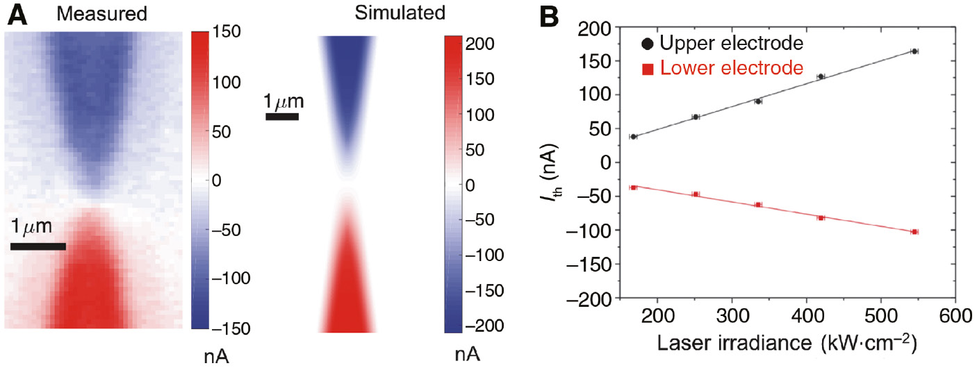
Thermocurrents at no bias.
(A) Thermocurrent maps at zero bias, Ith(x, y), obtained after scanning the structure under the laser focus (measured), and from simulation in the thermal and electromagnetic domains (simulated). (B) Dependence of the magnitude of the thermocurrent with incident laser power (data points) when the focal spot is located on either the upper electrode or lower electrode. The lines are linear fits to the data.
Locally, the amplitude of the contribution to the thermocurent is proportional to the temperature gradient in the geometry, and its sign is given by the direction of the temperature gradient relative to the location of the I/V converter in the circuitry. Hence, the overall current polarity of Ith depends whether the laser energy is absorbed by the upper or lower electrode. The sign of the detected current is represented by the color contrast in the map of Figure 3. In the present circuit configuration, the I/V converter is placed after the upper electrode. Thus, when the lower electrode is heated by the laser, the thermocurrent flows toward the upper lead and a positive current is measured. The situation is reversed when the laser is incident on the upper electrode. The thermal gradient flips and a negative current is detected. When the laser beam is centered on the constriction, heating is symmetric on either side and the net thermocurrent is null. We neglected any contribution to the current resulting from optical rectification because the electrical characteristic of the device is linear. Furthermore, the size of the constriction being relatively large, we did not observe any laser-induced modifications of the its shape during the measurement.
With numerical simulations, we generate a map of the thermocurrent Ith(x, y) by considering the individual temperature maps, Tlocal(u, v), and computing the contributions of each point on the structure to the total current for every location of the laser spot. The result is the simulated map displayed in Figure 3A, which qualitatively and quantitatively reproduces the experimental image of the current.
As long as the local temperature of the irradiated region is linear with incident laser intensity, the thermocurrent Ith is expected to follow the same trend. Figure 3B displays the magnitude of Ith when the laser is placed on either side of the constriction as a function of the incident laser intensity (data points). The position of the beam was adjusted to maximize the thermoresponse according to the Ith(x, y) map displayed in Figure 3A. The solid lines are linear fits to the data and confirm the thermal origin of the measured current.
5 Thermocurrent at Vb≠0 V
Applying a d.c. voltage to the constriction changes the system considerably. The d.c. Ib circulating through the constriction increases its global temperature via Joule dissipation. This is pictured by the simulated temperature maps presented in Figure 2A for Vb=+24 mV and for three laser positions. The thermal simulation predicts that the local temperature increases by 9 K at the location of the neck. This value is comparable to ΔTlocal given by the laser alone when Vb=0 mV. The overall change in temperature, when parameterized by the averaged value along the profile, is also increased by about 4.3 K with almost no dependence on the location of the laser spot.
As Joule dissipation and the corresponding temperature distribution are symmetric with respect to the geometry of the system [29], there is no net thermoelectric current generated by the applied bias. However, in the presence of the laser, symmetry breaks for excitation points located on either side of the constriction. To identify the resulting laser-induced Ith from the total current, we take advantage of the lock-in detection by extracting the component of the current synced at the chopper frequency fchop modulating the laser. Figure 4 shows the maps of the demodulated thermocurrent Ith(x, y) for different biases together with the simulated thermocurrents obtained with the same biasing conditions.
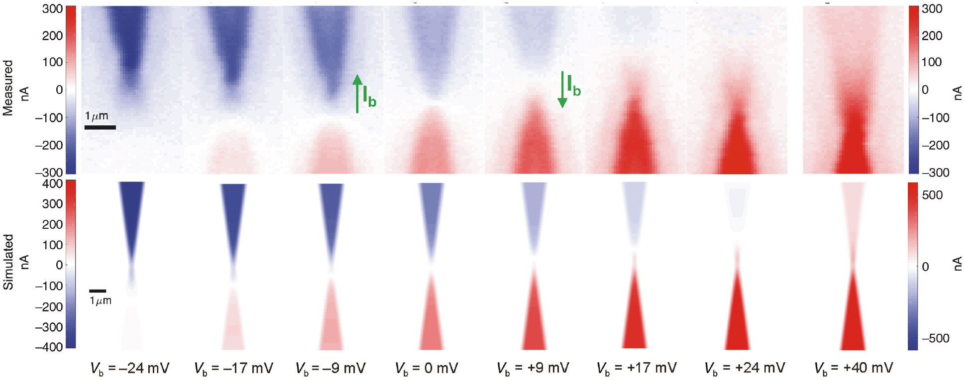
Thermocurrents maps with applied bias.
Measured thermocurrents are shown in the first row as a function of the bias voltage (see value on the top of the maps), between Vb=–24 mV and Vb=+24 mV, plus an additional measurement at Vb=+40 mV. The second row shows the thermocurrents numerically calculated for the same values of the bias voltage. The potential is applied to the lower electrode and the upper one is connected to the circuit ground. The green arrows at Vb=±9 mV indicate the direction of the electronic current Ib flowing in the device upon biasing.
Let us first consider the case where Vb=0 mV in the first row of Figure 4. This map should be compared to the map acquired by monitoring directly the output of the I/V converter displayed in Figure 3A. In our experimental setup, the sign inversion when the laser heats either side of the constriction is extracted from the phase output ψ(x, y) of the lock-in amplifier and is encoded in the color contrast of the image. The phase of the thermocurrent undergoes the expected 180° shift as the laser excites the upper or lower electrode leading to a change of the color contrast. The inversion point, located at the constriction, is precisely the center of symmetry of the system. In Figure 4, this phase provides the sign to the value of the modulus obtained from the lock-in amplifier.
Biasing the device while scanning the laser excitation changes significantly its thermoelectrical response. A voltage-induced electronic current is now circulating simultaneously to the laser-induced thermal current. This particular situation may be encountered in functional devices such as biased optical rectennas and hot-electron-harvesting Schottky barriers. Previous reports predicted that a circulating electronic current may counterbalance the effect of a thermally induced charge flow [30]. The symmetry of Ith(x, y) with respect to the constriction breaks when a small Vb is applied. Figure 4 illustrates the effect of a positive and negative bias on Ith(x, y). Let us consider Vb>0 when the potential is applied to the lower electrode, and the upper electrode is left at ground. The d.c. Ib circulates from the source electrode to the drain electrode as pictured by the green arrow in the column corresponding to Vb=+24 mV. The thermal current produced when the laser illuminates the source electrode decreases as the bias voltage increases. At Vb=+24 mV, the thermocurrent is completely suppressed if the laser illuminates the source portion of the constriction (upper electrode). The opposite effect happens if the drain electrode is heated by the laser. At Vb=+24 mV, Ith increases by twofold at the drain electrode. Let us refer to the threshold voltage canceling the thermocurrent in the source electrode as VT. We reproduce this behavior for negative biases when source and drain electrodes are swapped. At Vb=−24 mV, Ith has indeed increased by a factor 2 at the upper electrode, whereas no signal is detected when the laser is focused on the lower electrode.
We have seen above how thermal currents can be generated and accounted for when a temperature gradient is established along the structure at zero bias. Past research demonstrated that, in the absence of an external laser illumination, Joule dissipation generates a symmetric temperature distribution [29]. Hence, the biasing current does not produce a net thermoelectric current. Now, if the laser is turned on and scanned over the sample, the heat flow distribution generated by the bias voltage is combined to the heat flow produced by the laser itself. The rate and direction of the flow of heat is governed by Joule dissipation and by the presence of current and the existence of a temperature gradient along the structure under test. A simple calculation provides a value of about 1.7 mA of d.c. when 24 mV are applied over a 14 Ω element. Even if the overall resistance of the circuit is taken into account (~150 Ω), the circulating d.c. remains several orders of magnitude larger than the experimental and computationally evaluated thermocurrent Ith. The lock-in detection, synced with the laser illumination, filters out the d.c. effect of the biasing. The observation of a voltage-dependent thermocurrent when the laser excitation is asymmetric with respect to the constriction suggests the presence of an effect driven by thermoelectricity. This thermoelectric contribution is modeled as an additional term [see Eq. (3)] that modifies how the available charge carriers contribute to the total thermocurrent under biasing.
Joule heating is generally the dominant contribution in metals. However, the lock-in detection enables us to investigate the evolution of heat imposed by the local laser excitation generating a temperature gradient and an associated thermocurrent. Let us consider, for instance, the case of Vb=+9 mV in Figure 4. For an excitation of the source electrode, the thermocurrent has decreased from ~130 nA at zero bias to ~60 nA. In this case, the thermal gradient in the constriction is opposite to the electrical d.c. Ib. Carriers transport thermal energy to the drain electrode and the source electrode cools down. When the laser scans the lower electrode at Vb=+9 mV, the temperature gradient and the d.c. bear the same sign and heat is produced. Another interesting case happens when Vb=+VT=+24 mV in Figure 4. Here, the thermocurrent produced by the laser on the source electrode is completely suppressed by the d.c. voltage. This thermocurrent doubles its no bias value when the laser overlaps the drain electrode. The situation is exactly reversed when Vb=−VT as illustrated in Figure 4.
Previously, we showed that measuring the constriction resistance provides an indirect estimation of the temperature rise (Figure 3). Hence, thermoelectrical cooling and heating should manifest themselves as an asymmetric distribution of ΔR(x, y) with respect to the constriction. Figure 5 maps ΔR(x, y) when Vb=VT=+24 mV. The distribution clearly indicates a different constriction resistance whether the laser illuminates either of the electrodes. The decrease (increase) of ΔR(x, y) at the upper (lower) portion of the device is consistent with the thermocurrent map in Figure 4 for this bias voltage. However, because at Vb=VT the current vanishes on the upper electrode, we should expect no variation of ΔR(x, y) when the laser excites the upper electrode. It is clearly not the case, and this discrepancy arises from the measurement protocol of ΔR, which requires the application of an additional Vac bias summed up to the d.c. voltage Vb. In contrast, the alternating current produced by Vac cannot contribute to a net thermoelectric effect; it certainly contributes to Joule dissipation because the amplitude of Vac is roughly the same as VT.
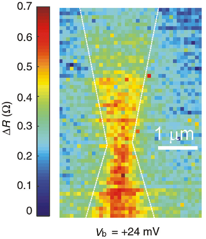
Map of the constriction resistance ΔR(x, y) when the structure is scanned through the focus for Vb=+24 mV.
ΔR(x, y) is lower when the laser illuminates the upper electrode than the bottom one.
The last column in Figure 4 is the thermoelectric current when Vb=+40 mV, a bias larger than VT. Joule dissipation in this case is close to the one produced when Vac is added to Vb=VT, which is the situation discussed previously. When the laser is absorbed by the lower electrode (drain), the thermocurrent is increased by a factor ~1.5 compared to its value at VT. Concomitantly, the thermocurrent is no longer canceled at the top electrode and a signal of 60 nA is measured. The color contrast stays constant indicating that the thermocurrent does not change direction. We therefore conclude that thermocurrents generated when the laser is focused on the upper part of the structure are drifted toward the drain due to biasing. Another effect that may reinforces this behavior is at higher voltage; the increase in temperature due to Joule dissipation modifies the laser absorption cross-section as the dielectric permittivity of gold changes [31]. Therefore, more absorption means more carriers seeing a larger temperature gradient and a resulting larger thermocurrent.
6 Dependencies of VT
In this section, we discuss the parameters influencing the threshold bias voltage VT for which the thermocurrent is suppressed in one lead and doubled in the other one. Incidentally, the value VT=24 mV corresponds approximately to the thermal voltage Vth of an electron near room temperature (eVth=kBT, with e is the electron charge and kB as the Boltzmann constant). Both biasing the device and laser absorption are contributing to elevate the temperature, but the increment remains modest (few Kelvin).
In the previous section, we correlated the contrast in Ith(x, y) maps at Vb=±VT to the potential an electron needs to acquire to gain an energy equal to the thermal energy kBT. Now, in this section, we link this behavior to the analysis of the actual voltage drop along the constriction. Both interpretations are compatible because the explanation given previously works with global parameters (Vb, TG, Imax). In this section, we scrutinize the local behavior the system.
The bias voltage Vb is applied to the entire electrical circuit consisting of resistors in series, including contributions inherent to the cables, connectors, contacts, in-plane electrodes, and finally the constriction. The potential drop at the constriction is thus a fraction of the applied bias. The total resistance sets the current density circulating in the constriction. This current density contributes to the local temperature distribution that influences the generation of a temperature gradient, modifying the thermocurrent due to the laser absorption. Hence, VT depends on the intrinsic electrical characteristics of the constriction. Another important parameter that may affect the value of VT is the local temperature reached at the laser focus, which impacts the thermocurrent. This can be tested by varying the laser intensity as shown in Figure 3B.
To make our point clearer, we fabricated a series of constrictions with varying widths to change their resistance. Rconstr are evaluated by a four-probe measurement to get rid off the resistance brought by the circuitry. The explored range is situated between 9 and 20 Ω. In Figure 6, we plot the effective voltage dropped at the constriction
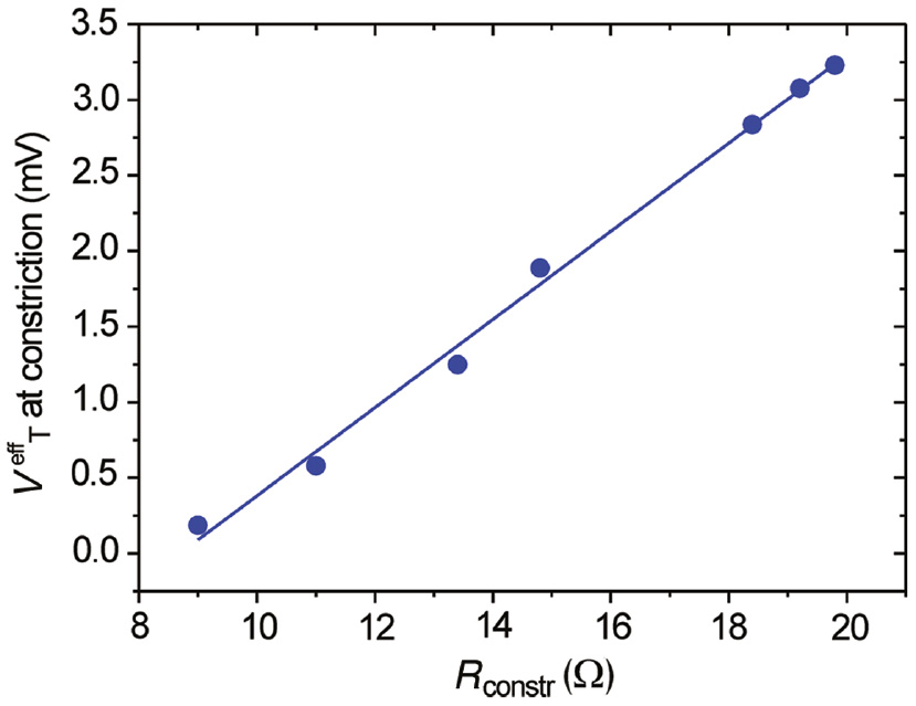
Evolution of the effective threshold voltage canceling the thermocurrent in one lead as a function of the constriction resistance.
The line is a linear fit to the experimental data. The laser intensity remains fixed at 500 kW cm−2.
For consistency with our experimental results, let us take the constriction already considered above. For a 14 Ω structure, the voltage drop required to nullify Ith is ~1.5 mV. We can make a rough estimate of the absolute temperature of the system when both the bias and the laser are applied. According to the simulation of Figure 2A, the overall temperature of the upper electrode when the laser is at 3.5 μm above the constriction is at about 12 K above room temperature (considered at 293 K). This particular point is located within the experimental area where we measure Ith~0 at Vb=VT (see Figure 4). This temperature corresponds to an electron thermal potential of 26.2 mV, which is 1.1 mV above that of an electron at room temperature. Noting that the temperature is inhomogeneous in the electrode, this estimate remains close to
7 Conclusions
The recent development of nanoscale light-harvesting metal devices provides an interesting venue for carrier generation and extraction. Our study shows that an optical laser excitation of a generic nanostructure, such as a nanoscale gold constriction, induces currents originating from thermoelectrical mechanisms within the device. We confirm a recent report showing that, even for a constriction made of the same material, thermocurrents are generated when heat is asymmetrically deposited on the device. A computational model of the thermoelectric effect reproduces the experimental results, supporting both the absorption characteristics of the metal structure and the thermoelectrical origin of the measured currents.
We demonstrate that an external bias voltage applied to the constriction considerably modifies the laser-driven thermal response. The results show how the drifted charge carriers set in motion by the temperature gradient respond to the external bias by moving in average preferentially towards the drain electrode of the constriction. We have found a value for the biasing voltage that cancels out the thermal current when the laser illuminates the source electrode. The observed experimental results have been modeled and simulated with good agreement.
The results described in this paper open the way for a better understanding of the thermoelectric signals generated on nanostructures illuminated under asymmetric conditions. The response of the device shown in this paper explains how an external voltage may drive thermocurrents vanishing or enhancing selectively the spatial responsivity of the device.
Acknowledgments
The work was funded by the European Research Council under the European Community’s Seventh Framework Program FP7/2007-2013 Grant Agreement 306772. Samples were fabricated using the nanofabrication facility of the technological platform ARCEN-Carnot financially supported by the Région Bourgogne Franche-Comté. The authors thank Irene Alda for her critical reading of the manuscript.
References
[1] Buret M, Uskov AV, Dellinger J, et al. Spontaneous hot-electron light emission from electron-fed optical antennas. Nano Lett 2015;15:5811–8.10.1021/acs.nanolett.5b01861Search in Google Scholar PubMed
[2] Kern J, Kullock R, Prangsma JC, Emmerling M, Kamp M, Hecht B. Electrically driven optical antennas. Nat Photonics 2015;9:582.10.1038/nphoton.2015.141Search in Google Scholar
[3] Parzefall M, Bharadwaj P, Jain A, Taniguchi T, Watanabe K, Novotny L. Antenna-coupled photon emission from hexagonal boron nitride tunnel junctions. Nat Nanotechnol 2015;10:1058–63.10.1038/nnano.2015.203Search in Google Scholar PubMed
[4] Gurunarayanan SP, Verellen N, Zharinov VS, et al. Electrically driven unidirectional optical nanoantennas. Nano Lett 2017;17:7433–9.10.1021/acs.nanolett.7b03312Search in Google Scholar PubMed
[5] Ittah N, Noy G, Yutsis I, Selzer Y. Measurement of electronic transport through 1G0 gold contacts under laser irradiation. Nano Lett 2009;9:1615–20.10.1021/nl803888qSearch in Google Scholar PubMed
[6] Ward DR, Hüser F, Pauly F, Cuevas JC, Natelson D. Optical rectification and field enhancement in a plasmonic nanogap. Nat Nanotechnol 2010;5:732–6.10.1038/nnano.2010.176Search in Google Scholar PubMed
[7] Stolz A, Berthelot J, Mennemanteuil M-M, et al. Nonlinear photon-assisted tunneling transport in optical gap antennas. Nano Lett 2014;14:2330–8.10.1021/nl404707tSearch in Google Scholar PubMed
[8] Emboras A, Niegemann J, Ma P, et al. Atomic scale plasmonic switch. Nano Lett 2016;16:709–14.10.1021/acs.nanolett.5b04537Search in Google Scholar PubMed
[9] Du W, Wang T, Chu H-S, Nijhuis CA. Highly efficient on-chip direct electronic–plasmonic transducers. Nat Photonics 2017;11:623.10.1038/s41566-017-0003-5Search in Google Scholar
[10] Dasgupta A, Mennemanteuil M-M, Buret M, Cazier N, Colas-des-Francs G, Bouhelier A. Optical wireless link between a nanoscale antenna and a transducing rectenna. Nat Commun 2018;9:1992.10.1038/s41467-018-04382-7Search in Google Scholar PubMed PubMed Central
[11] Wang F, Melosh NA. Power-independent wavelength determination by hot carrier collection in metal-insulator-metal devices. Nat Commun 2013;4:1711.10.1038/ncomms2728Search in Google Scholar PubMed
[12] Brongersma ML, Halas NJ, Nordlander P. Plasmon-induced hot carrier science and technology. Nat Nanotechnol 2015;10:25–34.10.1038/nnano.2014.311Search in Google Scholar PubMed
[13] Zheng BY, Zhao H, Manjavacas A, McClain M, Nordlander P, Halas NJ. Distinguishing between plasmon-induced and photoexcited carriers in a device geometry. Nat Commun 2015;6:7797.10.1038/ncomms8797Search in Google Scholar PubMed PubMed Central
[14] Grafström S. Photoassisted scanning tunneling microscopy. J Appl Phys 2002;91:1717.10.1063/1.1432113Search in Google Scholar
[15] Fumeaux C, Herrmann W, Rothuizen H, De Natale P, Kneubühl FK. Mixing of 30 THz laser radiation with nanometer thin-film Ni-NiO-Ni diodes and integrated bow-tie antennas. Appl Phys B 1996;63:135–40.10.1007/BF01095263Search in Google Scholar
[16] Ofarim A, Kopp B, Möller T, et al. Thermo-voltage measurements of atomic contacts at low temperature. Beilstein J Nanotechnol 2016;7:767–75.10.3762/bjnano.7.68Search in Google Scholar PubMed PubMed Central
[17] Zolotavin P, Evans C, Natelson D. Photothermoelectric effects and large photovoltages in plasmonic Au nanowires with nanogaps. J Phys Chem Lett 2017;8:1739–44.10.1021/acs.jpclett.7b00507Search in Google Scholar PubMed
[18] Baffou G. Thermoplasmonics: heating metal nanoparticles using light. Cambridge, Cambridge University Press, 2017.10.1017/9781108289801Search in Google Scholar
[19] Boriskina SV, Cooper TA, Zeng L, et al. Losses in plasmonics: from mitigating energy dissipation to embracing loss-enabled functionalities. Adv Opt Photonics 2017;9:775.10.1364/AOP.9.000775Search in Google Scholar
[20] Emboras A, Alabastri A, Ducry F, et al. Atomic scale photodetection enabled by a memristive junction. ACS Nano 2018;12:6706–13.10.1021/acsnano.8b01811Search in Google Scholar PubMed
[21] Roy D, Vignale G, Di Ventra M. Viscous corrections to the resistance of nanojunctions: A dispersion relation approach. Phys Rev B 2011;83:075428.10.1103/PhysRevB.83.075428Search in Google Scholar
[22] Briones E, Briones J, Cuadrado A, et al. Seebeck nanoantennas for solar energy harvesting. Appl Phys Lett 2014;105:093108.10.1063/1.4895028Search in Google Scholar
[23] Uskov AV, Khurgin JB, Buret M, Bouhelier A, Smetanin IV, Protsenko IE. Biased nanoscale contact as active element for electrically driven plasmonic nanoantenna. ACS Photonics 2017;4:1501–5.10.1021/acsphotonics.7b00272Search in Google Scholar
[24] Mennemanteuil M-M, Buret M, Cazier N, et al. Remote plasmon-induced heat transfer probed by the electronic transport of a gold nanowire. Phys Rev B 2016;94:035413.10.1103/PhysRevB.94.035413Search in Google Scholar
[25] Herzog JB, Knight MW, Natelson D. Thermoplasmonics: quantifying plasmonic heating in single nanowires. Nano Lett 2014;14:499–503.10.1021/nl403510uSearch in Google Scholar PubMed
[26] Fuchs K. The conductivity of thin metallic films according to the electron theory of metals. Math Proc Camb Philos Soc 1938;34:100108.10.1017/S0305004100019952Search in Google Scholar
[27] Zhang W, Brongersma S, Richard O, et al. Influence of the electron mean free path on the resistivity of thin metal films. Microelectron Eng 2004;76:146.10.1016/j.mee.2004.07.041Search in Google Scholar
[28] Cusack N, Kendall P. The absolute scale of thermoelectric power at high temperature. Proc Phys Soc 1958;72:898.10.1088/0370-1328/72/5/429Search in Google Scholar
[29] Ward DR, Halas NJ, Natelson D. Localized heating in nanoscale Pt constrictions measured using blackbody radiation emission. Appl Phys Lett 2008;93:213108.10.1063/1.3039060Search in Google Scholar
[30] Dubi Y, Di Ventra M. Colloquium: heat flow and thermoelectricity in atomic and molecular junctions. Rev Mod Phys 2011;83:131.10.1103/RevModPhys.83.131Search in Google Scholar
[31] Reddy H, Guler U, Kildishev AV, Boltasseva A, Shalaev VM. Temperature-dependent optical properties of gold thin films. Opt Mater Express 2016;6:2776–802.10.1364/OME.6.002776Search in Google Scholar
©2018 Alexandre Bouhelier et al., published by De Gruyter, Berlin/Boston
This work is licensed under the Creative Commons Attribution-NonCommercial-NoDerivatives 4.0 License.
Articles in the same Issue
- Review Articles
- High-efficiency broadband light coupling between optical fibers and photonic integrated circuits
- Plasmonic particle-on-film nanocavities: a versatile platform for plasmon-enhanced spectroscopy and photochemistry
- Coupling configurations between extended surface electromagnetic waves and localized surface plasmons for ultrahigh field enhancement
- Research Articles
- Laser-induced thermoelectric effects in electrically biased nanoscale constrictions
- Photonic spin Hall effect of monolayer black phosphorus in the Terahertz region
- On-chip optical parity checker using silicon photonic integrated circuits
- Stretchable and self-healable organometal halide perovskite nanocrystal-embedded polymer gels with enhanced luminescence stability
- Synthesis of few-layer 2H-MoSe2 thin films with wafer-level homogeneity for high-performance photodetector
- Aberration correction for improving the image quality in STED microscopy using the genetic algorithm
- Electroluminescence and photo-response of inorganic halide perovskite bi-functional diodes