Integrated Piezoelectric Energy Harvesting and Organic Storage System
-
Mohammad Y. Al-Haik
 und
Muhammad R. Hajj
und
Muhammad R. Hajj

Abstract
An experimental investigation of an integrated piezo-electric based energy harvester and an organic energy storage device is performed. The energy is harvested from a vibrating composite unimorph beam. The storage device is made out of an organic semiconductor material and storage elements from synthesized nanoparticles. The semiconducting polymer is obtained by blending poly (vinyl alcohol) and poly (acrylic acid) in crystal state polymers with sorbitol acting as the plasticizer. Zinc-Oxide nanoparticles with a diameter size between 50 and 70 nm are used as charge storage elements. A piezoelectric energy generation element made out of macro-fiber composite is used to harvest the energy from the vibrating beam. The harvested energy is stored in the organic capacitor. The performance of the organic device is evaluated through its comparison with commercial capacitors. The results show that the voltage produced was high enough to store the harvested energy in the organic capacitor. The charge and energy levels of the organic capacitor are reported.
Introduction
Ambient vibrations, generated by machines and biological systems, have been proposed as an energy source that can be exploited to harvest energy. Although small in magnitude, the harvested energy can be used to power small devices or to develop self-powered sensors and actuators that can be used in wireless sensor networks for monitoring purposes. The use of piezoelectric materials, such as macro-fiber composite (MFC) and lead zirconate titanate (PZT), to harvest storable energy from ambient vibrations is a well-developed research area (Williams et al. 2002; Priya and Inman 2009). Although it provides a good alternative to using batteries and in spite of continuous advancements to enhance the performance of electromechanical parameters through grain texturing (Yan et al. 2014), piezoelectric based energy harvesting remains limited by the low levels of available energy, low level of harvested energy due to the low efficiency of transduction mechanisms and more importantly by the input fluctuations which results in highly intermittent harvested power. To overcome these limitations, the energy harvester can be complemented with an energy storage device that can be used to ensure continuous operation of self-powered systems.
Umeda, Nakamural, and Ueha (1996) investigated the transformation of impact energy to electrical energy using a piezoelectric vibrator/actuator. They impacted a piezoelectric plate with a steel ball and measured the levels of produced energy. They also investigated the storage capabilities of the PZT-harvested energy with a rectifier and a capacitor. Sodano et al. (2003) used energy generated from ambient vibrations with two different types of piezoelectric actuators (PZT and MFC) to recharge a discharged nickel metal hydride battery. Recently, advancements have been made in the development of organic energy storage devices that use nanoparticles as charge storage elements (Ayesh et al. 2013; Al-Haik 2012). Such devices can be optimized to provide high density, high speed, low power, and low cost energy storage systems. Of particular importance is that they can be easily processed and manufactured into organic capacitors. Ma et al. (2003) fabricated a two-terminal electrical bistable device using a sandwich organic-metal-organic structured between two electrodes; an anode and cathode. The authors reported that the fabricated device was able to store the charge generated through the nanoclusters embedded within the organic layers. Their results were verified with experimental data that show electrical hysteresis behavior for the current-voltage curves. Mabrook et al. (2008) constructed metal-insulator-semiconductor (MIS) memory devices on silicon substrate with gold (Au) gold nanoparticles as the charge storage elements embedded between three different organic dielectric materials; polymethylmethacrylate, pentacene and cadmium arachidate. The fabricated MIS memory devices were characterized using C-V measurements. The results showed hysteresis loop plots that revealed charging and discharging characteristics regardless of the silicon substrate used, depending on the voltage range applied.
Organic capacitors, such as the ones investigated in this study, do not have the adverse effects of lithium ion batteries in terms of environmental contamination or potential for fires and explosions. Another advantage is that they can be embedded into printed circuit boards which can help in decreasing the size of the electronic devices (Kim et al. 2014). Furthermore, they are cost effective and extremely easy to manufacture and do not require a clean room for the fabrication process. Therefore, in this work, we experimentally investigate the integration of a piezo-electric energy device with an organic storage element as an energy harvesting/storage system. The energy is harvested from a macro-fiber composite (MFC) bonded to a vibrating beam-mass system. Conventional spin coating, vacuum-evaporating films and layer-by-layer sequential deposition/adsorption films were used in the fabrication of the organic storage device. Our objective is to assess the effectiveness of combining these two components of energy harvesting and storage and specific aspects of the integrated system that need to be considered in its development.
Experimental Setup
Energy Harvesting
The experimental setup for the energy harvesting consisted of an MFC piezo element that was bonded to a composite beam. The beam, with a mass attached to its tip, was mounted on a shaker as shown in Figure 1. A frequency sweep was applied in order to determine the region of parametric resonance of the beam. The natural frequency of the beam is 8 Hz. The range for effective parametric resonance was determined to be between 15.90 and 16.10 Hz. The amplitude of the signal driving the shaker was fairly small to simulate the vibrations of a beam that can be attached to structures, building, appliances and equipment. Table 1 presents the properties and dimensions of the macro-fiber composite. The piezoelectric actuator was positioned approximately 1 cm away from the clamped area.
Properties and size of the MFC patch.
| Parameter | Value |
| Material density | 7,800 (Kg/m3) |
| MFC type | d33 |
| Strain permittivity | 15.9 (nF/m) |
| Active length | 40 (mm) |
| Active width | 10 (mm) |
| Thickness | 0.26 (mm) |
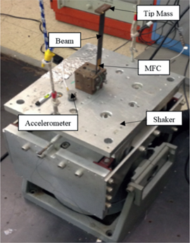
Experimental setup of the beam mass system as mounted on the shaker.
Energy Storage
The preparation of the semiconducting blend polymer is described by Josh et al. (2013). Briefly, poly-vinyl alcohol (PVA) and poly-acrylic acid (PAA) with average molecular weights of 61,000 g/mol and 5,000,000 g/mol, respectively, were used. Each polymer solution was produced by stirring 5 g of each polymer separately in 100 ml of deionized water. Each mixture was stirred at 90 °C using a magnetic stirrer until it showed a clear homogeneous jelly type substance that is free of air bubbles. The solution was then left to cool down for one hour. Then, 10 ml of each of the PVA and PAA solutions were mixed together with 2 weight percent (wt%) of sorbitol, which acts as the plasticizer and was chosen because of its high conductivity, texture and ease of formability. This mixture was subjected to vigorous mixing to ensure a homogenous texture. Membranes of PVA-PAA-sorbitol were obtained using the solution casting technique (Mohsin, Hossin, and Haik 2011; Ayesh et al. 2012). Herein, 20 ml of the mixture was casted onto a PTFE plate to form a thin film and left inside an oven set to 60 °C and left overnight. The membranes were then tested for their dryness, free standing, and uniformity of thickness. The films were also used to determine the conductivity by analyzing their resistivity. The poly (methyl methacrylate) (PMMA) solution was prepared by diluting 24 mg of PMMA powder (molecular weight 97,000 g/mol) in 3 ml of chloroform and left overnight under stirring to ensure a perfect dissolution.
Results
Figure 2 depicts the scanning electron microscopy (SEM) image which shows clusters of ZnO nanoparticles uniformly distributed over the entire substrate. It was observed that these large clusters of nanoparticles contain smaller nanoparticles and was verified by using a Malvern Instruments Zeta analyzer that precisely determined the diameter size of each individual nanoparticle, which was found to vary between 50 and 70 nm as seen in Figure 3. During the SEM testing, the ZnO nanoparticles were noticed to glow (see Figure 2), implying that the nanoparticles are charging due to the high electron voltage applied by the SEM.
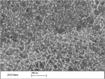
Scanning electron microscopy (SEM) image of the ZnO nanoparticles.
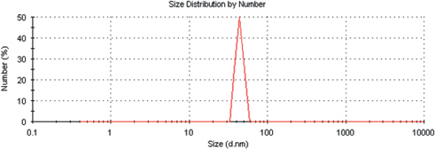
Zeta analyzer for ZnO nanoparticles: Average particle diameter size roughly 55 nm.
The electrical characteristics of the semiconducting blend were investigated by Al-Haik (2012). Figure 4 depicts the impedance curve measurements of the polymer blend. The two semicircles indicate that the impedance of the blend has the same characteristics as those a pair of parallel RC circuits connected in series as shown in Figure 5. The first semi-circle, assigned to the charge transfer process (kinetic process) that occurs at high frequencies, corresponds to the resistive and capacitive components of the film, denoted by Rfilm and Cfilm. The second semi-circle, which corresponds to the contribution of mass migration process, diffusion, and occurs at low frequency range, is related to the interfacial charge transfer resistance and double layer capacitance, denoted by Rct and Cdl. The resistance values Rfilm and Rct were used to calculate the resistivity of the semiconducting blend. The results showed that adding the sorbitol significantly lowered the resistivity of the blend; from 3.28 × 10⁵ KΩm to 2.21 × 10³ KΩm (Al-Haik 2012). This decrease in resistivity implies that adding sorbitol increased the conductivity significantly.
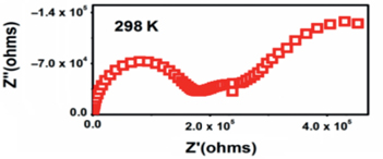
AC impedance spectra for PVA-PAA- 2 wt% Sorbitol measured at room temperature.
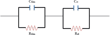
Equivalent circuits of the two semicircle Nyquist plot.
Figure 6(A) and 6(B) show a schematic of the layer-by-layer setup of the organic capacitor and a picture of the fabricated device as tested, respectively. The fabrication of the organic capacitor was carried out as followed: Glass substrates of dimensions 2 cm × 2 cm were cleaned by the standard cleaning method inside an ultrasonic cleaner using acetone, ethanol and deionized water (one after the other for repeated times), and then dried with nitrogen gas. The bottom electrode of the device was created by depositing aluminum (Al) film with a thickness of 100 nm on the glass substrates using thermal evaporation. Then, the PMMA solution was spin coated on the substrate (on the Al electrode) initially at 500 r/min for 10 s, then at 5,000 r/min for 50 s. Afterwards, the sample was annealed at 120 °C for 20 min.
The zinc oxide (ZnO) nanoparticles were synthesized by chemical co-precipitation technique. The nanoparticles had an average diameter size that varied between 50 and 70 nm. These particles were obtained by dissolving 0.314 g zinc acetate and 0.48 g NaOH in 330 ml ethanol. The mixture was then refluxed at 60 °C for 1 h. The reaction between the acetate group and the base yielded the conversion of the zinc acetate into zinc oxide. After reaction, the zinc oxide ethanol dispersion was mixed with DI-water for purification. The ZnO particles were then separated from the dispersion supernatant by centrifugation at 7,000 r/min for 5 min repeatedly. Finally, the ZnO nanoparticles were dispersed in ethanol and sonicated for 30 s to obtain the ZnO-ethanol dispersion.
The ZnO nanoparticles were then spread over the PMMA layer by spin coating for 90 s at a speed of 5,000 r/min, and dried on a hotplate at 50 °C. The polymer blend of PVA-PAA-sorbitol was spin coated at 5,000 r/min for 2 min and dried at 80 °C for 5 min. A shadow mask consisting of an array of 2 mm diameter circular holes was used to fabricate an array of aluminum top electrodes by thermal evaporation with a thickness of 100 nm.
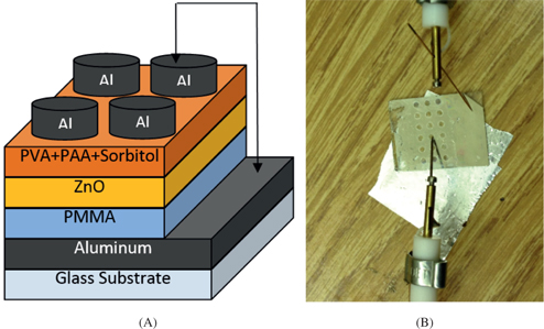
Layer-by-layer schematic of the device (A) and picture of the organic capacitor with the connection setup (B).
Capacitance-voltage (C-V) sweeps on the storage device with zinc oxide nanoparticles and on a reference device that did not contain these particles were conducted. The measurements were performed with a dual voltage sweep between –20 V and +20 V at a scan rate of 1 V/s and a frequency of 100 kHz. Figure 7(A) shows a C-V plot for a reference device that does not contain the layer of ZnO nanoparticles. Figure 7(B) shows the C-V plot for the organic capacitor with embedded ZnO nanoparticles. This plot shows the conventional accumulation and inversion characteristics that are similar to a typical metal-insulator-semiconductor device. This hysteresis was not observed in Figure 7(A). As such, the hysteresis can be attributed to the ability of the ZnO nanoparticles to trap electrons, which indicates their capability to act as a capacitor.
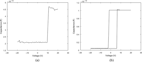
C-V characteristics of: (A) a reference device that does not contain ZnO nanoparticles that shows no hysteresis and (B) a device with embedded ZnO nanoparticles that shows a hysteresis loop between ±5 V.
Integrated Unimorph and Device System
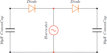
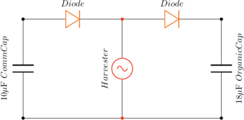
Figures 8 and 9, show circuit diagrams of the carried out experiments. Figure 8 shows the setup when using two commercial capacitors, having a capacitance of 10 μF. Figure 9 shows a similar circuit diagram but with one of the commercial capacitors replaced by the organic capacitor. As the shaker moves, the beam vibrates. The piezoelectric patch then converts the mechanical vibration into electrical energy. As the voltage is generated and current flows through the diodes, the capacitors are charged.
Circuit diagram of two commercial capacitors having a capacitance of 10 μF.
Circuit diagram of both organic and commercial capacitors.
Discussion
Two sets of experiments were performed. In one set, the harvester was connected to two commercial capacitors each with a capacitance of 10 μF. Two diodes were introduced in the circuit configuration to capture the positive voltage by one capacitor and the negative voltage by the other capacitor. The voltages generated by the MFC patch and across each of the two capacitors were measured. The results are plotted in Figure 10. The plot shows that the voltage generated by the beam varied between ±4.5 V with a period that corresponds to the natural frequency of the beam. The voltage across the capacitor shows that the capacitor charges instantly. Additionally, small variations near a mean value of 4 V are noticed. The cause of these variations is discusses below in more details. Basically, they correspond to small charging and discharging activities as the beam oscillates and negative and positive voltages are generated. As the current flows in the circuit, the capacitor charges. Once the current reverses its direction because of the reverse in the strain associated with the beam’s motion, the diode stops it from flowing. At that instant, the capacitor starts to discharge. A small amount of the charge is actually discharged during the reverse motion of the beam. The capacitor starts to charge again when the beam motion is reversed and the current is flowing through the diode.
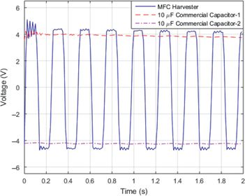
Measured voltages across the energy harvester and two commercial capacitors.
To test the effectiveness of the organic capacitor, we replaced one of the commercial capacitors with the organic capacitor and repeated the experiments. The results are plotted in Figure 11. It is interesting to note that the performance level of the ZnO storage element is equivalent to that of the commercial capacitor. Because a constant voltage of about 4 V is maintained across the capacitor, the maximum level that can be generated by the piezoelectric element is just over this limit. The reason is the circuit setup as shown in Figure 9. The small difference is attributed to the voltage lost across the diode and connections. Furthermore, the time constant of the capacitor is large enough that the capacitors do not show a significant voltage drop as the sign of the harvested voltage changes that causes the current to stop flowing through it as a result of the diode. For that reason the voltage across the capacitor appears to remain more or less constant.
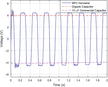
Measured voltages across the energy harvester, the organic capacitor and a 10 μF commercial capacitor.
The small variations in the voltage across the capacitors are better exhibited in the plot presented in Figure 12(A) and 12(B) that shows these variations over a smaller duration. The cut-off of the peak of the harvester is due to the allowable voltage across the capacitor. The hysteresis loop in Figure 7(B) shows the C-V measurement for the organic storage device having a maximum voltage between ±5 V, which implies that the maximum allowable voltage to enter the capacitor is limited to this voltage range. The dotted lines in both figures show the charging and discharging activities as the beam moves back and forth. In both cases, the discharge starts when the voltage/current generated by the piezoelectric element starts to decrease, i. e. when the beam moves from its maximum position (peak). The charge starts again when the beam changes direction from the negative strain to positive strain allowing the current to pass through the diode again and instantly charges the capacitor. Because the discharge rate is very low, the discharge levels are very small in both cases. Both organic and commercial capacitors are shown to hold a constant charge as the beam oscillates back and forth. We should note that while these characteristics are similar there is a slight difference in the time constant of both capacitors. This is due to the fact that the internal resistance of the commercial capacitor is about three times larger than that of the organic capacitor.
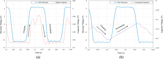
Expended sections of Figure 11 that show the charging and discharging for (A) the organic capacitor and (B) a 10 μF commercial capacitor as the beam generates charge.
The charge stored in the fabricated organic capacitor was measured to be 68.7 μC, where the capacitance of the fabricated capacitor was 18.09 μF, measured by using a multifunctional digital multimeter. The thickness of the semiconducting polymer and PMMA layers were averaged to be 16.6 μm with a contact area of, A = 3.14 mm2; which yields a charge density of 1.32 C/mm3. One way to increase the charge is to change the permittivity of the capacitor. Hence, increasing the electrode contact area is essential to increasing the storage capability of the organic capacitor. Adding more contact electrode points is another approach to increase the storage capacity. Also, increasing the ZnO nanoparticles size would most definitely increase the capacitance since they are the major contributors to the storage. The disadvantage of carrying out this approach is that the surface roughness will increase and most likely effect the top aluminum layer that will be sputtered over the layers. Using the values of C and V, the energy stored in the capacitor is determined; 1.31 × 10⁻⁴ J, which yields an energy density of 2.51 J/mm3. The layer-by-layer setup for fabricating the organic capacitor required the use of a mechanical mask to be placed on the very top of the device to deposit the aluminum layer (the top electrode). These electrodes are 2 mm in diameter and the gate point to contact is much smaller. Therefore, there is the possibility of increasing the storage capacity by increasing the number of contact points without a need to increase the overall area of the capacitor.
Conclusions
We assessed the effectiveness of using an organic capacitor to store energy harvested by a piezo-electric patch attached to a vibrating composite beam. The experimental results showed that the organic capacitor has a performance that is comparable to that of a commercial capacitor. The voltage generated from the MFC actuator was high enough to enable storage of the generated charge. The storage capacity in terms of the charge and energy levels was also determined. Based on the C-V characteristics of the organic capacitor and other measurements, procedures for enhancing the performance of the organic capacitor were suggested.
References
Al-Haik, M. Y. 2012. “Conductive Polymer Blends and Their Use in Memory Devices.” MSc thesis, United Arab Emirates University, Al-Ain, UAE.Suche in Google Scholar
Ayesh, A. I., M. A. Mohsin, M. Y. Al-Haik, and Y. Haik. 2012. “Investigations on Electrical Properties of Poly(Vinyl Alcohol) Doped with 1-Methyl-3-n-Decyl-Imidazolium Bromide Ionic Liquid.” Current Applied Physics 12 (4):1223–8.10.1016/j.cap.2012.03.004Suche in Google Scholar
Ayesh, A. I., S. Qadri, V. J. Baboo, M. Y. Al- Haik, and Y. Haik. 2013. “Nano-Floating Gate Organic Memory Devices Utilizing Ag–Cu Nanoparticles Embedded in PVA-PAA-Glycerol Polymer.” Synthetic Metals 183:24–8.10.1016/j.synthmet.2013.09.018Suche in Google Scholar
Josh, V., M. Y. Al-Haik, A. I. Ayesh, M. A. Mohsin, and Y. Haik. 2013. “Electrical Properties of Sorbitol Doped PVA-PAA Polymer Membranes.” Journal of Applied Polymer Science 128 (6):3861–9.10.1002/app.38619Suche in Google Scholar
Kim, J. S., J. M. Han, M. R. Joung, S. H. Kweon, C. Y. Kang, J. H. Paik, Y. H. Jeong, and S. Nahm. 2014. “Ca0. 15zr0. 85O1. 85 Thin Film for Application to MIM Capacitor on Organic Substrate.” Energy Harvesting and Systems 1 (3–4):243–50.10.1515/ehs-2014-0010Suche in Google Scholar
Ma, L. P., S. Pyo, J. Ouyang, Q. F. Xu, and Y. Yang. 2003. “Nonvolatile Electrical Bistability of Organic/Metal-Nanocluster/Organic System.” Applied Physics Letters 82:607–9.10.1063/1.1556555Suche in Google Scholar
Mabrook, M. F., C. Pearson, D. Kolb, D. A. Zeze, and M. C. Petty. 2008. “Memory Effects in Hybrid Silicon-Metallic Nanoparticle-Organic Thin Film Structures.” Organic Electronics 9:816–20.10.1016/j.orgel.2008.05.023Suche in Google Scholar
Mohsin, M. A., A. Hossin, and Y. Haik. 2011. “Thermal and Mechanical Properties of Poly(Vinyl Alcohol) Plasticized with Glycerol.” Journal of Applied Polymer Science 122 (5):3102–9.10.1002/app.34229Suche in Google Scholar
Priya, S. and D. J. Inman, eds. 2009. Energy Harvesting Technologies, vol. 21. New York: Springer.10.1007/978-0-387-76464-1Suche in Google Scholar
Sodano, H. A., G. Park, D. J. Leo, and D. J. Inman. 2003. “Use of Piezoelectric Energy Harvesting Devices for Charging Batteries.” Smart Structures and Materials 5050:101–8.10.1117/12.484247Suche in Google Scholar
Umeda, M., K. Nakamural, and S. Ueha. 1996. “Analysis of the Transformation of Mechanical Impact Energy to Electric Energy Using Piezoelectric Vibrator.” Japanese Journal of Applied Physics 35:3267–73.10.1143/JJAP.35.3267Suche in Google Scholar
Williams, R. B., G. Park, D. J. Inman, and W. K. Wilkie. 2002. “An Overview of Composite Actuators with Piezoceramic Fibers.” Proceeding of IMAC XX, 4–7 February 2002.Suche in Google Scholar
Yan, Y., A. Marin, Y. Zhou, and S. Priya. 2014. “Enhanced Vibration Energy Harvesting Through Multilayer Textured Pb (Mg1/3nb2/3) O3–PbZrO3–PbTiO3 Piezoelectric Ceramics.” Energy Harvesting and Systems 1 (3–4):189–95.10.1515/ehs-2014-0001Suche in Google Scholar
©2016 by De Gruyter
Artikel in diesem Heft
- Frontmatter
- Articles
- Integrated Piezoelectric Energy Harvesting and Organic Storage System
- Design Considerations for Optimal Absorption of Energy from a Vibration Source by an Array of Harvesters
- Efficient Nonlinear Energy Harvesting with Wrinkled Piezoelectric Membranes
- Micro Wind Turbine for Powering Wireless Sensor Nodes
- Autonomous Flyback Converter for Energy Harvesting from Microbial Fuel Cells
- An Approach to a Flexible Thermoelectric Generator Fabricated using Bulk Materials
- Magnetoelectric Alternator
- Giant Magnetoelectric Effect in PZT Thin Film Deposited on Nickel
- Triboelectric Power Generation from Paper Vibration Induced by Sonic Waves