Near-field optics for nanoprocessing
-
Mitsuhiro Terakawa
Mitsuhiro Terakawa received his BS, MS and PhD degrees from Keio University in 2003, 2005 and 2007, respectively. In 2007, he joined the Wellman Center for Photomedicine, Massachusetts General Hospital, Harvard Medical School, as a research fellow. Currently, he is an Associate Professor at Keio University. His research interests include ultrafast laser processing, laser processing of biomaterials, laser drug delivery, and laser-based nanostructure formation.
 und
Nikolay N. Nedyalkov
und
Nikolay N. Nedyalkov
Nikolay N. Nedyalkov received his MS degree from Sofia University, Physical Department, in 1998. In 2005, he received his PhD from the Bulgarian Academy of Sciences, Institute of Electronics. He worked on laser nanostructuring and plasmonics during his post doc position and visiting researcher at Keio University for total 3 years in the period 2005–2015. His current position is professor at Institute of Electronics, Bulgarian Academy of Sciences. His work is focused on laser-matter interaction, laser nanostructuring, and plasmonics.

Abstract
The recent progress in laser processing reaches a level where a precise fabrication that overcomes the diffraction limit of the far-field optics can be achieved. Laser processing mediated by enhanced near field is one of the attractive methods to provide highly precise structuring with a simple apparatus. In this review, we describe the fundamentals of the electromagnetic near field in the vicinity of small structures and the application of its specific properties for nanomodification. Theoretical and experimental results on nanoablation based on electromagnetic field enhancement due to plasmon polariton excitation and Mie scattering are discussed. High-throughput nanohole fabrication mediated by arrayed nanospheres is discussed, as the coupling effect of near field is also considered. In addition, recent fabrication techniques and their potential applications in nanopatterning, nanoscale deformation, and biophotonics are discussed.
1 Introduction
Laser processing technology has shown rapid and robust development in industrial applications based on scientific understandings. It should be noted that the utilization of a femtosecond laser has provided precise and intense laser processing of various kinds of materials, which is realized by the photon energy confinement in an ultrashort period of time [1, 2]. To improve the processing performance or to create new innovations, two major continuous efforts in laser processing have been made: ‘how precise’ and ‘how efficient’ (processing throughput). For the former challenge, several methods have been proposed to overcome the theoretical resolution limit of laser processing determined by Abbe’s criterion. Laser fabrication in subdiffraction-limited spatial resolution was demonstrated by non-linear multiphoton absorption, which took advantage of the Gaussian spatial profile [3]. Nanohole fabrication on a GaN surface is also demonstrated by using the second harmonic of a near-infrared femtosecond laser [4]. Laser processing mediated by enhanced near field is one of the most promising methods to realize high-precision processing to meet the demand. Photon energy confinement in terms of spatial distribution has widely been known at present by the development of near-field optics, and the localized interaction zone in nanoscale overcomes the diffraction limit, which provides highly precise fabrication especially with a synergistic effect by using the femtosecond laser. For the latter challenge, fabrication methods of multiple subwavelength structures were demonstrated by a single pulse illumination, e.g. the formation of periodic patterns by using a simple apparatus [5, 6].
Laser irradiation of nanostructures such as nanospheres and nanotips excites enhanced electromagnetic (EM) field in nanospace. Besides the optical properties observed in the far field, the nature of the near field defines a significant decrease of the optical intensity with the distance from the surface of the nanostructures, enabling the interaction in the submicro to the nano scale. The excited near field shows large dependency for the presence of target materials, as we describe in this review. It is essential to discuss the interaction with target materials for the understanding of laser processing with enhanced near field. The laser processing properties, therefore, should be discussed not only with the excitation of near field, but also with the coupling effect of the near field. In this review, the fundamentals of enhanced near field will be described followed by that of nanoablation by using a single small structure for near-field excitation. High-throughput nanostructure formation by simultaneous ablation with arrayed nanospheres, i.e. nanopatterning, will be discussed with the coupling effect of near field. In addition, recent fabrication techniques based on the near-field processing will be introduced. Bioapplications will also be described as the recent and emerging applications of laser nanoprocessing.
2 Enhanced optical near field
Being an object of fundamental modern physics as materials with ‘unusual’ properties related to size-dependent electron energy states, nanostructures found practical application centuries ago [7, 8]. Romans used these properties to fabricate pieces of art such as the dichroic Lycurgus cup. The specific extinction spectra of gold nanoparticles having an intense peak in the visible region give a brilliant ruby color used to decorate glasses in cathedrals in the 17th century. More than a hundred years ago, in 1908, Gustav Mie explained the phenomena by solving Maxwell’s equations for the absorption and scattering of the EM radiation by spherical particles. It becomes clear that the decrease of the particle size at dimensions smaller than the illuminated optical wavelength can contribute to a resonant excitation of collective electron oscillations (plasmon polariton) in these structures. The plasmon excitation influences their far-field optical properties, giving sharp resonances in absorption and scattering spectra, which are not present in bulk material. In the near-field zone, the EM intensity could be significantly enhanced, and due to its evanescent characteristics light ‘focusing’ at dimensions defined by the metal nanostructure size rather than the far-field optical components can be achieved.
The qualitative interpretation of the response of a particle to the incident EM field can be easily presented in the case of dipole or quasi-static approximation. In such an assumption, which is applied when the size of the particle is at least an order of magnitude smaller than the EM field wavelength, the incident wave induces coherent oscillations of the electron system over the particle (Figure 1). The properties of the EM field components for such system can be described as for an oscillating dipole [9]. For an incident plane wave, the components of the EM field are
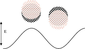
A schematic representation of the interaction of a small metal particle with EM field. Assuming that the heavy ion system is static, the electrons oscillate following the incident E field.
These expressions show a dependence on the parameter kr=r/r0, which is equal to 1 when r=r0=λ/2π. In the zone where r<<r0, referred to as the near-field zone, the dominant component is proportional to 1/r3 as it is present only in the electric field component. Thus, the field in the near-field zone is expressed by the electric component, and its amplitude can be significant with the decrease of r, i.e. approaching the dipole (Figure 2).
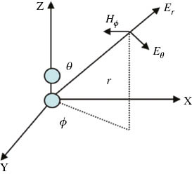
Components of the EM field presented in Eq. (1).
In the dipole approximation, the particle polarizability can be expressed as
where ε and εm are the dielectric functions of the particle with radius R and the environment, respectively. The polarizability of particle has a resonance when |ε(ω)+2εm |=(ε1(ω)+2εm)2+(ε2(ω))2 is minimal. If the dielectric function of the environment is a constant in the considered spectral range, and ε1(ω) and ε2(ω) are the real and imagined parts of the particle dielectric function, this condition can be satisfied at ε1(ω)=-2εm , as ε2 <<1.
The rigorous solution to the problem of the interaction of a spherical particle with the EM field is given by G. Mie. In his work, the Maxwell equations in spherical coordinates are solved with appropriate boundary conditions [10]. The electric and magnetic components of the incident and resulting field are presented using multipole expansions. The scattered field components (Es , Hs ) and the extinction (Cext ), scattering (Csca ), and absorption (Cabs ) cross sections are given by
with
where
On the basis of these equations, the far-field optical properties of spherical particles can be obtained.
Messinger et al. developed the solution of the scattering problem considering the effects in the close vicinity of the particle surface [11]. The near-field scattering efficiency, Qnf , defined as a ratio between the power scattered in the near-field zone to the incident one for a given geometrical cross section, is given by
where
The application of Eq. (5) to metal particles expresses a resonance behavior representing plasmon excitations as the resonance wavelength depends on the particle characteristics. As the near field consists of evanescent components, the resonances are shifted with respect to the corresponding ones in the far-field zone. At resonance conditions, the Qnf can be orders of magnitude >1, representing the local field enhancement close to the particle surface. With the increase of the particle size, excitation of higher modes is realized, as the dipole mode is shifted to longer wavelengths due to the retardation effect. Equation (5) can be used for the definition of the optimal conditions for near-field intensity enhancement for a given particle size and environment dielectric function.
In the case of dielectric particles, the optical response includes the EM field scattered out and inside the particle. The extinction cross section as a function of the parameter x may consist of sharp peaks, with a value >1 expressing enhancement of the EM field. These originate from superposition of different excited modes l. For large particles (R>λef ), the particle efficiently focuses the incident irradiation, which can be sufficient for local modification of the underlying surface. With the decrease of the particle size, the focusing ability decreases. In a low-size regimen, the contribution of low-order scattering modes defines the characteristics of the EM in the near-field zone [12]. The EM field properties can be significantly modified by changing the dielectric properties of the particle. It is shown that for dielectric particles with a high refractive index, the field enhancement at the resonances can exceed that observed for the corresponding Au nanoparticle [13].
The recent developments in powerful computer systems and numerical approaches for the description of the interaction between the EM field and nanostructures, like the finite-difference time-domain (FDTD) and discrete dipole approximation, brought more light to the specific properties of the EM field in the near-field zone. It is found that the spatial characteristics of the zone with the enhanced field intensity depend on the incident field properties, geometry of irradiation, environment dielectric properties, and the presence of neighbor nanoparticles [14–19].
3 Nanoablation
The optical near field is proportional to r-3 of the scattering amplitude of the scattered EM field. The optical near field provides not only localization of light energy in a small space but is also accompanied by enhancing light intensity, which is the key phenomenon for laser processing. Localized laser ablation occurs in a limited zone in which the enhanced laser energy exceeds the threshold. By tuning the optical intensity distribution, precise laser ablation is achieved in the localized spot. As the use of femtosecond laser significantly reduces the heat-affected zone, its combination with the near-field enhancement can provide efficient processing with high resolution.
As the area of enhanced near-field intensity is strongly confined to the illuminated structure surface, structures whose sizes are smaller than the incident wavelength can be used to generate enhanced optical near field for nanosized processing. As for a pen-writing-like scheme, two structures are used: an apertureless pointed tip and an aperture tip. The former case uses tips for atomic force microscope (AFM) or scanning tunneling microscope (STM). The latter case uses a probe tip for a near-field scanning optical microscope. The enhanced near field on the tip depends on the geometry of the tip structure, incident wavelength, incident angle, and distance between the tip and the target substrate surface. A pioneering work was reported by Jersch and Dickmann by using an STM tip to treat metal surface in air in 1996 [20]; however, a question has arisen on whether the surface modification is attributable to the near-field enhancement or a mechanical contact due to the transient tip expansion [21]. The thermal expansion of the tip at the laser irradiation is still challenging in this technique because the near-field intensity drastically decreases with increasing distance from the surface of the nanostructure, resulting in the difficulty in precise positioning of the tip [22, 23]. Although there are difficulties in tip positioning and the processing throughput is lower, high preciseness is an advantage of this technique. Chimmalgi et al. demonstrated fabrication of grooves whose width is 10–50 nm on metal thin films by irradiating a silicon tip placed above the surface with femtosecond laser pulses at a wavelength of 800 nm [24]. Periodically modified metal structures support propagating plasmons that at specific geometries may result in field localization at a specific location. Using such a system, Srituravanich et al. developed a nanolithography system that is capable of high-speed nanostructuring [25]. The same group used a periodic nanohole two-dimensional (2D) array for parallel structuring of photoresist [26].
Metallic nanospheres show attractive properties to generate intense optical near field. Unlike nanoprocessing using nanotip, which requires accurate configuration and precise adjustment of tip-to-substrate distance, nanoprocessing with metallic spheres requires only deposition of spheres on the substrate surface. The distribution of the enhanced near field around a sphere is governed by the plasmon polariton as described above; however, the EM field is largely affected by the electromagnetic coupling between the metallic sphere and the substrate. This results in a strong enhancement of the field intensity in the contact point of the sphere and the substrate. The coupling is due to the capacitive interaction of the near field around the sphere and the image charge induced in the substrate (Figure 3). Figure 4 shows optical intensity distribution around a gold sphere irradiated in vacuum (A) or on a silicon substrate (B). The intensity distribution was calculated by the FDTD method. Strong optical near field is generated on the contact point of the sphere and the substrate surface (B), while the distribution characteristic for dipole oscillation is dominant in the case of vacuum (A). The strong enhancement on the contact point contributes to nanoablation on the substrate surface. The localization of the near field in the vicinity of the contact point between the particle and the substrate strongly depends on the dielectric properties of the latter. For metal or dielectric substrates with a high refractive index, the zone with enhanced field intensity localizes in the contact point even when the polarization of the incident irradiation is parallel to the substrate surface [14]. The oscillation direction of electrons depends on the polarization of the incident laser pulse; thus, the enhanced optical field on the substrate surface will depend on the polarization. This results in a change of the shape of nanoholes created on the surface by changing the polarization of the incident irradiation (Figure 5). The influence of the polarization and the specific spatial distribution of the near field in the vicinity of metal nanoparticles are used also for fabrication of holes with non-circular geometry by using incident irradiation at different than normal to the surface substrate incidence [15]. The strong confinement of the zone with the enhanced near-field intensity to the particle surface results in a decrease of the enhanced field area size with a decrease of the particle diameter. FDTD simulation shows that the specific width of the enhanced field area could be several times smaller than the particle diameter [28]. This indicates that the size of the enhanced field area and, respectively, the produced structure dimensions can be controlled by the particle size. Based on this fabrication of nanoholes with a size of λ/20, using 40-nm gold particles is demonstrated [29]. Metallic nanoparticles whose shape is not spherical have also been used for near-field processing. Hunbenthal et al. fabricated nanochannels by using arrayed gold nanotriangles on glass substrate irradiated by femtosecond laser pulse [30]. Harrison et al. used gold nanorods with tuning aspect ratio to fabricate nanoholes [31]. Leiderer et al. used the modification induced by the near-field enhancement in vicinity of spherical and triangle particles for visualization of the near-field spatial characteristics [32].
Conceptual illustration of EM coupling between a metallic sphere and a substrate.
![Figure 4: Optical field intensity (|E/E0|2) distribution for a 200-nm gold sphere (A) in vacuum and (B) on silicon substrate. The 800-nm incident wave polarization is linear and the E vector is parallel to the x axis [27].](/document/doi/10.1515/aot-2015-0054/asset/graphic/j_aot-2015-0054_fig_004.jpg)
Optical field intensity (|E/E0|2) distribution for a 200-nm gold sphere (A) in vacuum and (B) on silicon substrate. The 800-nm incident wave polarization is linear and the E vector is parallel to the x axis [27].
![Figure 5: SEM images of the fabricated nanohole with 200-nm gold sphere on silicon substrate. The pulse duration is 150 fs, laser fluence is 0.2 J/cm2, and the hole is ablated by a single shot irradiation. (A) and (B) show the hole obtained with circular polarization and linear polarization, respectively. The inset shows the optical field intensity distribution inside the Si substrate (z=-1.25 nm) [27].](/document/doi/10.1515/aot-2015-0054/asset/graphic/j_aot-2015-0054_fig_005.jpg)
SEM images of the fabricated nanohole with 200-nm gold sphere on silicon substrate. The pulse duration is 150 fs, laser fluence is 0.2 J/cm2, and the hole is ablated by a single shot irradiation. (A) and (B) show the hole obtained with circular polarization and linear polarization, respectively. The inset shows the optical field intensity distribution inside the Si substrate (z=-1.25 nm) [27].
Dielectric nanospheres are promising candidates as well to generate enhanced optical field. In their work on laser cleaning of silicon substrate, Luk’yanchuk et al. reported nanohole formation on the substrate [33]. Irradiation of 500-nm silica nanospheres on the substrate using nanosecond laser pulses resulted in the formation of a hillock of 100 nm in diameter at laser fluences below the ablation threshold for the bulk material. As in the presented experiments, the size of the sphere was smaller compared to the laser wavelength, and the spheres are deposited onto the substrate; the authors concluded that the spheres behaved as scatterers that generate enhanced near field, resulting in nanohole ablation, instead of the possibility to act as a far-field microlens. Münzer et al. compared nanohole fabrication with nanosecond laser and femtosecond laser and reported that femtosecond laser provides precise laser ablation with a limited heat affected zone [12]. For the nanoablation using a dielectric sphere, the size parameter (α=2πR/λ, R: radius of the sphere, λ: incident wavelength), defined in the Mie scattering theory, is a critical parameter for the properties of the generated near-field light. Figure 6 shows the dependence of the near-field efficiency Qnf at the sphere surface on the size parameter for four wavelengths: 800 nm (fundamental wave of Ti:sapphire femtosecond laser), 400 nm (SHG), 263.5 nm (THG), and 200 nm [34]. At the incident wavelength of 263.5 nm, the near-field efficiency decreases with the increasing size parameter due to the optical absorption by the polystyrene (PS) sphere itself, which can be understood by the increase of the material extinction coefficient k at shorter wavelengths. Wang et al. proposed near-field laser ablation in liquid using 5-μm silica spheres on glass substrate [35]. The focusing point under the sphere was tuned due to the change in the relative refractive index. Drawing of lines, star-like structures, and alphabets were also demonstrated with oblique irradiation of multiple pulses [36, 37]. The theoretical investigation was also reported on the temporal dynamics of near field around dielectric microparticle excited by femtosecond laser pulse [38].
![Figure 6: Dependence of the near-field efficiency on the size parameter for four wavelengths [34]. The near-field efficiency Qnf is starting from α=0.01.](/document/doi/10.1515/aot-2015-0054/asset/graphic/j_aot-2015-0054_fig_006.jpg)
Dependence of the near-field efficiency on the size parameter for four wavelengths [34]. The near-field efficiency Qnf is starting from α=0.01.
The mechanisms playing role in nanoablation in the presence of enhanced near field are not clearly understood yet. A simple interpretation could be related to the strong heating of the metal nanoparticle or the lens effect, and localization of the scattered field induced by dielectric particles that will trigger thermal ablation mechanisms, such as evaporation, non-equilibrium phase explosion, fragmentation, or stress-induced material removal, when ultrashort laser pulses are applied. For metal nanoparticles on a dielectric substrate with a low refractive index, the heating of particles is considered to be triggering the nanohole formation [14, 39]. However, in the cases of strong localization of the near field in the contact point between the particle and substrate, the presence of additional mechanisms could be considered. The material removal in this case is accompanied by the presence of strongly enhanced electric field. Furthermore, the performed experiments demonstrate a strong relation of the hole shape to the spatial distribution of the enhanced field zone. It is shown that the presence of a strong electric field may induce ionization, atom and electron emission from the particle and the substrate [40, 41], leading to a permanent substrate modification. In addition, the presence of electric field in the vicinity of a sharp metal structure and conductive substrate may generate tunnel currents that could induce resistive heating of the substrate and subsequent local structuring [40].
The thermal and near-field enhancement-related mechanisms for surface modification may play a different role for given processing conditions. The maximum in the absorption spectra, which is related to the efficient heating of the particle, generally do not coincide with the maximum of the near-field scattering efficiency. In the case of gold, the contribution of d and sp band electronic transitions defines high absorption at wavelengths lower than about 530 nm, and the absorption peak position for spherical particles exhibits a weak dependence on the particle size [11]. In the wavelength range from 520 to 900 nm, the imaginary part of the complex refractive index of gold is low [42], contributing to the possibility of efficient excitation of plasmon modes in this spectral range and efficient near-field scattering. Thus, the change of the particle size results in an efficient shift of the plasmon resonance even in the infrared region of the spectrum, which can result in the existence of enhanced field intensity in the particle vicinity.
4 Nanopatterning
One of the attractive advantages in sphere-mediated near-field ablation is high-throughput fabrication of multiple nanoholes by using arrayed spheres. The underlying physics are plasmon polariton and Mie scattering in the case of arrayed spheres, as similar to single sphere; however, the phenomenon attributed to closely aligned spheres is necessary to be considered. The capacitive coupling between the charges of adjacent spheres is a key factor to understand the optical properties, so as to understand the near-field processing in case of arrayed metallic spheres. A strong near field can be excited in the intersphere gap of closely spaced spheres. The spatial distribution and the magnitude of the optical near field are affected by intersphere interaction, i.e. plasmon coupling (Figure 7). The scattering cross section of a sphere in the array would also be affected due to the presence of the adjacent particles. Figure 8 shows the near-field intensity distribution on the gold substrate surface on which gold nanospheres with a diameter of 200 nm are arrayed hexagonally, and irradiated by a single laser pulse at a wavelength of 800 nm. The intensity distribution is shown for three different intersphere distances. When the spheres are in contact, the near-field intensity is comparably low on the surface; however, it is significant between particles.
Conceptual illustration of EM coupling between metallic spheres and a substrate.
![Figure 8: Calculated optical near-field intensity (|E/E0|2) distribution on a gold substrate surface when gold nanospheres with diameter of 200 nm are arrayed hexagonally and irradiated by optical wave at a wavelength of 800 nm. The field distribution is shown for three intersphere distances: (A) 200 nm (touching spheres), (B) 400 nm, and (C) 785 nm. The white circle represents the sphere delineation in (A) [43].](/document/doi/10.1515/aot-2015-0054/asset/graphic/j_aot-2015-0054_fig_008.jpg)
Calculated optical near-field intensity (|E/E0|2) distribution on a gold substrate surface when gold nanospheres with diameter of 200 nm are arrayed hexagonally and irradiated by optical wave at a wavelength of 800 nm. The field distribution is shown for three intersphere distances: (A) 200 nm (touching spheres), (B) 400 nm, and (C) 785 nm. The white circle represents the sphere delineation in (A) [43].
Arrayed dielectric spheres also show change in the near-field properties, compared to the isolated particles, but the effect is comparably low compared to the case of metallic spheres. Laser ablation using dielectric spheres is also known as laser nanosphere lithography or sphere-mediated laser ablation, and it is widely used for parallel nanostructuring [44–47]. In case of dielectric particles, the near-field properties are affected by interaction not only with surface charge induced in the spheres but also with the EM field inside the spheres. Sakai et al. reported fabrication of periodic nanohole array on silicon and glass substrate surfaces by using 2D arrayed PS spheres irradiated by femtosecond laser pulse [34]. Figure 9A and B show scanning electron microscopy (SEM) images of silicon substrate surface after irradiation of hexagonally arrayed PS spheres with single femtosecond laser pulse at wavelengths of 800 and 400 nm, respectively. Nanopatterning was also demonstrated for a silicon carbide [49] and a silicon dioxide layer [50]. A dielectric sphere with a high refractive index can also provide a strong near-field enhancement even for small size parameter due to Mie resonance scattering. Figure 10 shows intensity enhancement for hexagonally close-packed 200-nm sphere array deposited on Si substrate as a function of the sphere’s refractive index. The enhancement factors for 2D sphere arrays show peaks at around 2.1 and at 3.1, which are shifted from the case of a single sphere. Recently, David et al. experimentally imaged the complex optical near fields with monolayers of PS spheres by imprinting them on photosensitive films [52]. The fabrication of multiple and complex structures shows the potential of arrayed sphere-mediated laser processing toward tailor patterned structures.
![Figure 9: (A and B) SEM images of the Si surface after femtosecond laser irradiation. (A) 800 nm with fluence of 288 mJ/cm2; (B) 400 nm with fluence of 57 mJ/cm2. (C and D) SEM images of ordered monolayer PS spheres in hexagonal array on silicon substrate. (C) The diameter is 800 nm. (D) The diameter is 450 nm [48].](/document/doi/10.1515/aot-2015-0054/asset/graphic/j_aot-2015-0054_fig_009.jpg)
(A and B) SEM images of the Si surface after femtosecond laser irradiation. (A) 800 nm with fluence of 288 mJ/cm2; (B) 400 nm with fluence of 57 mJ/cm2. (C and D) SEM images of ordered monolayer PS spheres in hexagonal array on silicon substrate. (C) The diameter is 800 nm. (D) The diameter is 450 nm [48].
![Figure 10: Evaluated factors for intensity enhancement when the hexagonally close-packed sphere array with the diameter of 200 nm is placed on an Si substrate, as a function of the sphere’s refractive index (λ=400 nm) [51].](/document/doi/10.1515/aot-2015-0054/asset/graphic/j_aot-2015-0054_fig_010.jpg)
Evaluated factors for intensity enhancement when the hexagonally close-packed sphere array with the diameter of 200 nm is placed on an Si substrate, as a function of the sphere’s refractive index (λ=400 nm) [51].
5 Recent progress in near-field nanoprocessing
Near-field nanoprocessing using a sphere can be used for pen-like writing of nanostructures similar to tip-mediated methods by combination with optical trapping [53, 54]. Unlike optical trapping using Gaussian beam, Bessel beam provides the flexibility for the positioning of the sphere in vertical direction with respect to the substrate surface. In this case, self-positioning for keeping a constant sphere-to-substrate distance even for a non-flat surface can be achieved. Due to the good control of the distance, which is one of the key parameters for efficient structuring, this method may have high potential in fabrication of lines with a high width control.
Femtosecond laser irradiation of gold nanoparticles placed on a substrate can also create unique structures in addition to nanoholes, in a wide area around the particles. Figure 11 shows the surface structure obtained when gold nanoparticle placed on a silicon substrate surface is irradiated by femtosecond laser pulses. A circular ripple pattern can be seen around the spot where the gold nanoparticle was placed. The experimental result can be explained by an interference effect that is well consistent with EM field distribution simulation [55]. A similar nanostructure was also found with the case of a dielectric microsphere for both oblique and normal incidences using an excimer laser (Figure 12) [56, 57]. Those nanostructures are unique and attractive; however, still unrevealed physics, e.g. the origin of dotted substructure in the ripple in the case of gold nanosphere [55], remain.
![Figure 11: SEM image of the silicon surface after laser irradiation. The circularly polarized femtosecond laser at 400 nm was irradiated at 0.08 J/cm2. The two white circles are the 200-nm-diameter gold spheres. The interference period is 400 nm approximately [55].](/document/doi/10.1515/aot-2015-0054/asset/graphic/j_aot-2015-0054_fig_011.jpg)
SEM image of the silicon surface after laser irradiation. The circularly polarized femtosecond laser at 400 nm was irradiated at 0.08 J/cm2. The two white circles are the 200-nm-diameter gold spheres. The interference period is 400 nm approximately [55].
![Figure 12: Near-field pattern in PTT film generated by a silica microsphere after a single excimer laser pulse irradiation at an angle θ=54° (laser impinges from the left). (A) AFM topography map (25×25 μm2) and (B) zoom (5×4 μm2) and topography profile (below) along the red line in the backscattering region. The original position of the silica microsphere is marked by a dashed circle. Reprinted with permission from Ref. [56]. Copyright 2013 American Chemical Society.](/document/doi/10.1515/aot-2015-0054/asset/graphic/j_aot-2015-0054_fig_012.jpg)
Near-field pattern in PTT film generated by a silica microsphere after a single excimer laser pulse irradiation at an angle θ=54° (laser impinges from the left). (A) AFM topography map (25×25 μm2) and (B) zoom (5×4 μm2) and topography profile (below) along the red line in the backscattering region. The original position of the silica microsphere is marked by a dashed circle. Reprinted with permission from Ref. [56]. Copyright 2013 American Chemical Society.
Femtosecond laser processing is a powerful and reliable tool not only limited to material removal. The reduction of the heat-affected zone, and the strong time confinement of the interaction, gives opportunity for other attractive processing. One of the promising methods is nanoscale deformation by ultrafast plasmon localization. Femtosecond laser irradiation to preformed metallic nanostructure, which is smaller than the incident wavelength, excites localized plasmon followed by the localized melting at the plasmonic hotspot [58]. This technique is used for nanobump fabrication where femtosecond laser interaction enables the ultrafast melting phenomena in limited area, which results in partial melting and material deformation. Deformation using gold nanoprism [59] and nanostripe [60] is also reported.
6 Bioapplications of near-field processing
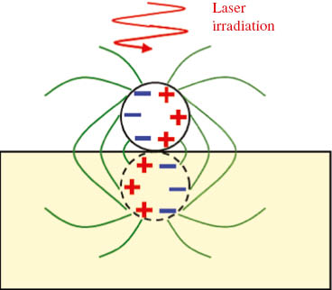
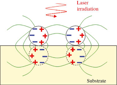
Recent developments in near-field processing opened a new avenue in the field of bioapplications as well. The interaction of laser pulse and nanoparticles has been used for decades for photothermal therapy, inactivation of microorganisms, tumor detection or treatment, biosensors, etc. One of the notable streams is the utilization of ultrashort pulsed lasers for the nanoprocessing of biomaterials, which attract growing interest recently. Ultrafast interaction and the localized interaction zone in nanoscale provided by ultrashort pulsed laser allow the treatment of cells with little effect on the survival rate. Schomaker et al. reported the cell membrane perforation and delivery of plasmid DNA to cultured cells in vitro by using gold nanoparticles dispersed around cells [61]. This method is called gold-nanoparticle-mediated laser transfection [62–64]. Meunier et al. investigated in detail the mechanism of near-field cell processing in water and reported that the shock wave generated around a gold nanoparticle after femtosecond laser irradiation is responsible for the rapid expansion of plasma instead of rapid increase of the gold nanoparticle temperature [65–67]. Simultaneous treatment of multiple cells and cell selectivity by an antibody-antigen interaction are significant advantages in this method. Recently, the interaction of ultrashort laser pulse and gold nanoparticle shows a wide variety of applications in cell stimulation and manipulation, such as the intracellular increase in calcium accompanied by an intracellular calcium wave after the gold-particle-mediated stimulation [68, 69]. Polymer spheres are also promising candidates for nanoprocessing of cell membrane [70–72]. The enhanced optical field generated under the polymer sphere perforates the cell membrane and enables to introduce exogenous molecules inside the cells (Figure 13). Fluorescent molecules and small interfering RNA were successfully introduced to cells by using polylactic acid (PLA) microsphere. PLA is one of the typical biodegradable polymers that are already used in clinical treatments.
![Figure 13: Conceptual diagram of biodegradable sphere-mediated perforation of a cell membrane using a femtosecond laser. The sphere works as a microlens, and a femtosecond laser irradiation generates a strongly enhanced optical field under the sphere to perforate the membrane [71].](/document/doi/10.1515/aot-2015-0054/asset/graphic/j_aot-2015-0054_fig_013.jpg)
Conceptual diagram of biodegradable sphere-mediated perforation of a cell membrane using a femtosecond laser. The sphere works as a microlens, and a femtosecond laser irradiation generates a strongly enhanced optical field under the sphere to perforate the membrane [71].
7 Conclusions
In this paper, laser nanoprocessing by near-field enhancement is reviewed from the fundamental of near-field optics to recent applications. The use of near field generated around nanoparticles is an attractive method to provide precise processing that overcomes the far-field diffraction limit. The method is capable of fabrication of nanoholes on various substrates, including metals, semiconductors, and dielectrics, and may offer a base of new technologies for photonics and electronics industries. Recent emerging techniques based on near-field processing, such as fabrication of circular patterns as well as nanoscale deformation, are also attractive for the fabrication of novel nanostructures. Near-field laser nanoprocessing opens new avenues not only for material removal or nanohole formation, but also for versatile manufacturing, fabrication, and stimulation techniques.
About the authors

Mitsuhiro Terakawa received his BS, MS and PhD degrees from Keio University in 2003, 2005 and 2007, respectively. In 2007, he joined the Wellman Center for Photomedicine, Massachusetts General Hospital, Harvard Medical School, as a research fellow. Currently, he is an Associate Professor at Keio University. His research interests include ultrafast laser processing, laser processing of biomaterials, laser drug delivery, and laser-based nanostructure formation.

Nikolay N. Nedyalkov received his MS degree from Sofia University, Physical Department, in 1998. In 2005, he received his PhD from the Bulgarian Academy of Sciences, Institute of Electronics. He worked on laser nanostructuring and plasmonics during his post doc position and visiting researcher at Keio University for total 3 years in the period 2005–2015. His current position is professor at Institute of Electronics, Bulgarian Academy of Sciences. His work is focused on laser-matter interaction, laser nanostructuring, and plasmonics.
Acknowledgments
The authors are grateful to Prof. Emeritus Minoru Obara of Keio University and Prof. Peter Atanasov of Bulgarian Academy of Sciences. The authors would also like to thank Drs. Tetsuo Sakai, Tomoya Miyanishi, and Yuto Tanaka for their contribution on the research. The authors wish to thank the support from Japan Society for the Promotion of Science, Program for Invitation Fellowships for Research in Japan (L15538).
Author contributions
M. T. and N. N. N. wrote the manuscript. M. T. and N. N. N. contributed equally to this work.
References
[1] K. Sugioka and Y. Cheng, Light Sci. Appl. 3, e149 (2014).10.1038/lsa.2014.30Suche in Google Scholar
[2] K. C. Phillips, H. H. Gandhi, E. Mazur and S. K. Sundaram, Adv. Opt. Photonics 7, 684 (2015).10.1364/AOP.7.000684Suche in Google Scholar
[3] S. Kawata, H. B. Sun, T. Tanaka and K. Takada, Nature 412, 697 (2001).10.1038/35089130Suche in Google Scholar PubMed
[4] S. Nakashima, K. Sugioka and K. Midorikawa, Appl. Phys. A 101, 475 (2010).10.1007/s00339-010-5947-ySuche in Google Scholar
[5] J. Bonse, J. Krüger, S. Höhm and A. Rosenfeld, J. Laser Appl. 24, 042006 (2012).10.2351/1.4712658Suche in Google Scholar
[6] Y. Nakata, T. Okada and M. Maeda, Appl. Phys. Lett. 81, 4239 (2002).10.1063/1.1522481Suche in Google Scholar
[7] M. Kerker, J. Colloid Interface Sci. 105, 297 (1985).10.1016/0021-9797(85)90304-2Suche in Google Scholar
[8] M. A. El-Sayed, Acc. Chem. Res. 34, 257 (2001).10.1021/ar960016nSuche in Google Scholar
[9] S. Kawata, M. Ohtsu and M. Irie, Near-Field Optics and Surface Plasmon Polaritons (Springer, Berlin, 2001).10.1007/3-540-44552-8Suche in Google Scholar
[10] G. Mie, Ann. Phys. 25, 377 (1908).10.1002/andp.19083300302Suche in Google Scholar
[11] B. J. Messinger, K. U. Raben, R. K. Chang and P. W. Barber, Phys. Rev. B 24, 649 (1981).10.1103/PhysRevB.24.649Suche in Google Scholar
[12] H. -J. Münzer, M. Mosbacher, M. Bertsch, J. Zimmermann, P. Leiderer, et al., J. Microsc. 202, 129 (2001).10.1046/j.1365-2818.2001.00876.xSuche in Google Scholar
[13] Y. Tanaka and M. Obara, Jpn. J. Appl. Phys. 48, 12R (2009).10.1143/JJAP.48.122002Suche in Google Scholar
[14] N. N. Nedyalkov, S. Imamova, P. A. Atanasov, Y. Tanaka and M. Obara, J. Nanopart. Res. 13, 2181 (2011).10.1007/s11051-010-9976-4Suche in Google Scholar
[15] T. Miyanishi, T. Sakai, N. N. Nedyalkov and M. Obara, Appl. Phys. A 96, 843 (2009).10.1007/s00339-009-5313-0Suche in Google Scholar
[16] N. N. Nedyalkov, R. G. Nikov and P. A. Atanasov, Proc. SPIE 8770, 877005 (2013).10.1117/12.2013200Suche in Google Scholar
[17] A. Plech, P. Leiderer and J. Boneberg, Laser Photon. Rev. 3, 435 (2008).10.1002/lpor.200810044Suche in Google Scholar
[18] D. Eversole, B. Luk’yanchuk and A. Ben-yakar, Appl. Phys. A 89, 283 (2007).10.1007/s00339-007-4166-7Suche in Google Scholar
[19] F. Moreno, B. García-Cámara, J. M. Saiz and F. González, Opt. Express 16, 12487 (2008).10.1364/OE.16.012487Suche in Google Scholar
[20] J. Jersch and K. Dickmann, Appl. Phys. Lett. 68, 868 (1996).10.1063/1.116527Suche in Google Scholar
[21] R. Huber, M. Koch and F. Feldmann, Appl. Phys. Lett. 73, 2521 (1998).10.1063/1.122502Suche in Google Scholar
[22] S. M. Huang, M. H. Hong, Y. F. Lu, B. S. Luk’yanchuk, W. D. Song, et al., J. Appl. Phys. 91, 3268 (2002).Suche in Google Scholar
[23] J. Boneberg, H. -J. Münzer, M. Tresp, M. Ochmann and P. Leiderer, Appl. Phys. A 67, 381 (1998).10.1007/s003390050789Suche in Google Scholar
[24] A. Chimmalgi, T. Y. Choi, C. P. Grigoropoulos and K. Komvopoulos, Appl. Phys. Lett. 82, 1146 (2003).10.1063/1.1555693Suche in Google Scholar
[25] W. Srituravanich, L. Pan, Y. Wang, C. Sun, D. B. Bogy, et al., Nat. Nanotech. 3, 733 (2008).10.1038/nnano.2008.303Suche in Google Scholar
[26] W. Srituravanich, N. Fang, C. Sun, Q. Luo and X. Zhang, Nano Lett. 4, 1085 (2004).10.1021/nl049573qSuche in Google Scholar
[27] Y. Tanaka, N. N. Nedyalkov and M. Obara, Appl. Phys. A 97, 91 (2009).10.1007/s00339-009-5354-4Suche in Google Scholar
[28] N. Nedyalkov, T. Sakai, T. Miyanishi and M. Obara, J. Phys. D Appl. Phys. 39, 5037 (2006).10.1088/0022-3727/39/23/021Suche in Google Scholar
[29] N. N. Nedyalkov, T. Miyanishi and M. Obara, Appl. Surf. Sci. 253, 6558 (2007).10.1016/j.apsusc.2007.01.025Suche in Google Scholar
[30] F. Hunbenthal, R. Morarescu, L. Englert, L. Haag, T. Baumert, et al., Appl. Phys. Lett. 95, 063101 (2009).10.1063/1.3186787Suche in Google Scholar
[31] R. K. Harrison and A. Ben-Yakar, Opt. Express 18, 22556 (2010).10.1364/OE.18.022556Suche in Google Scholar PubMed
[32] P. Leiderer, C. Bartels, J. König-Birk, M. Mosbacher and J. Boneberg, Appl. Phys. Lett. 85, 5370 (2004).10.1063/1.1819990Suche in Google Scholar
[33] Y. F. Lu, L. Zhang, W. D. Song, Y. W. Zheng and B. S. Luk’yanchuk, JETP Lett. 72, 457 (2000).10.1134/1.1339899Suche in Google Scholar
[34] T. Sakai, Y. Tanaka, Y. Nishizawa, M. Terakawa and M. Obara, Appl. Phys. A 99, 39 (2010).10.1007/s00339-010-5576-5Suche in Google Scholar
[35] Z. B. Wang, W. Guo, A. Pena, D. J. Whitehead, B. S. Luk’yanchuk, et al., Opt. Express 16, 19706 (2008).10.1364/OE.16.019706Suche in Google Scholar PubMed
[36] L. Li, W. Guo, Z. B. Wang, Z. Liu, D. Whitehead, et al., J. Micromech. Microeng. 19, 054002 (2009).10.1088/0960-1317/19/5/054002Suche in Google Scholar
[37] W. Guo, Z. B. Wang, L. Li, D. J. Whitehead, B. S. Luk’yanchuk, et al., Appl. Phys. Lett. 90, 243101 (2007).10.1063/1.2748035Suche in Google Scholar
[38] Y. E. Geints, E. K. Panina and A. A. Zemlyanov, J. Quant. Spectrosc. Radiat. Transfer 131, 146 (2013).10.1016/j.jqsrt.2012.11.025Suche in Google Scholar
[39] S. Hashimoto, T. Uwada, M. Hagiri and R. Shiraishi, J. Phys. Chem. C 115, 4986 (2010).10.1021/jp106830xSuche in Google Scholar
[40] J. B. Park, B. Jaeckel and B. A. Parkinson, Langmuir 22, 5334 (2006).10.1021/la053148aSuche in Google Scholar PubMed
[41] S. Kondo, S. Heike, M. Lutwyche and Y. Wada, J. Appl. Phys. 78 155 (1995).10.1063/1.360733Suche in Google Scholar
[42] U. Kreibig, M. Vollmer, Optical Properties of Metal Clusters (Springer, Berlin, 1995).10.1007/978-3-662-09109-8Suche in Google Scholar
[43] N. N. Nedyalkov, P. A. Atanasov and M. Obara, Nanotechnology, 18, 305703 (2007).10.1088/0957-4484/18/30/305703Suche in Google Scholar
[44] H.-J. Muenzer, M. Mosbacher, M. Bertsch, O. Dubbers, F. Burmeister, et al., Proc. SPIE 4426, 180 (2002).10.1117/12.456827Suche in Google Scholar
[45] C. Constantinescu, L. N. D. Kallepalli, P. Delaporte, O. Utéza and D. Grojo, Appl. Surf. Sci. 336, 112 (2015).10.1016/j.apsusc.2014.10.003Suche in Google Scholar
[46] A. Afanasiev, V. Bredikhin, A. Pikulin, I. Ilyakov, B. Shishkin, et al., Appl. Phys. Lett. 106, 183102 (2015).10.1063/1.4919898Suche in Google Scholar
[47] Z. B. Wang, M. H. Hong, B. S. Luk’yanchuk, Y. Lin, Q. F. Wang, et al., J. Appl. Phys. 96, 6845 (2004).10.1063/1.1786652Suche in Google Scholar
[48] M. Terakawa, M. Obara, Ultrafast Laser Processing: From Micro- to Nanoscale, Chapter 7 (Pan Stanford Publishing, Singapore, 2013).Suche in Google Scholar
[49] A. Battula, S. P. Theppakuttai and S. Chen, J. Microlith. Microfab. Microsyst. 5, 011009 (2006).Suche in Google Scholar
[50] D. Grojo, L. Boarino, N. De Leo, R. Rocci, G. Panzarasa, et al., Nanotechnology 23, 285305 (2012).10.1088/0957-4484/23/48/485305Suche in Google Scholar PubMed
[51] Y. Tanaka, G. Obara, A. Zenidaka, N. N. Nedyalkov, M. Terakawa, et al., Opt. Express 18, 27226 (2010).10.1364/OE.18.027226Suche in Google Scholar PubMed
[52] C. David, P. Kühler and F. J García de Abajo, J. Siegel, Opt. Exp. 22, 8226 (2014).10.1364/OE.22.008226Suche in Google Scholar
[53] E. McLeod and C. B. Arnold, Nat. Nanotech. 3, 413 (2008).10.1038/nnano.2008.150Suche in Google Scholar
[54] Y. C. Tsai, R. Fardel and C. B. Arnold, Appl. Phys. Lett. 98, 233110 (2011).10.1063/1.3598427Suche in Google Scholar
[55] G. Obara, Y. Tanaka, N. N. Nedyalkov, M. Terakawa and M. Obara, Appl. Phys. Lett. 99, 061106 (2011).10.1063/1.3624925Suche in Google Scholar
[56] I. Martín-Fabiani, J. Siegel, S. Riedel, J. Boneberg, T. A. Ezquerra, et al., ACS Appl. Mater. Interfaces, 5, 11402 (2013).10.1021/am4036543Suche in Google Scholar PubMed
[57] P. Kühler, F. J. García de Abajo, P. Leiprecht, A. Kolloch, J. Solis, et al., Opt. Express 20, 22063 (2012).10.1364/OE.20.022063Suche in Google Scholar PubMed
[58] V. K. Valev, D. Denkova, X. Zheng, A. I. Kuznetsov, C. Reinhardt, et al., Adv. Mater. 24, OP29 (2012).10.1002/adma.201103807Suche in Google Scholar
[59] S. Viarbitskaya, A. Cuche, A. Teulle, J. Sharma, C. Girard, et al., ACS Photonics, 2, 744 (2015).10.1021/acsphotonics.5b00100Suche in Google Scholar
[60] V. K. Valev, W. Libaers, U. Zywietz, X. Zheng, M. Centini, et al., Opt. Lett. 38, 2256 (2013).10.1364/OL.38.002256Suche in Google Scholar
[61] M. Schomaker, J. Baumgart, A. Ngezahayo, J. Bullerdiek, I. Nolte, et al., Proc. SPIE 7192 (2009).10.1117/12.809316Suche in Google Scholar
[62] D. Heinemann, M. Schomaker, S. Kalies, M. Schieck, R. Carlson, et al., PLoS ONE 3, e58604 (2013).10.1371/journal.pone.0058604Suche in Google Scholar PubMed PubMed Central
[63] S. Kalies, T. Birr, D. Heinemann, M. Schomaker, T. Ripken, et al., J. Biophotonics 7, 474 (2014).10.1002/jbio.201200200Suche in Google Scholar PubMed
[64] D. Heinemann, S. Kalies, M. Schomaker, W. Ertmer, H. Murua-Escobar, et al., Nanotechnology 24, 245101 (2014).10.1088/0957-4484/25/24/245101Suche in Google Scholar PubMed
[65] A. Robitaille, E. Boulais and M. Meunier, Opt. Express 21, 9703 (2013).10.1364/OE.21.009703Suche in Google Scholar PubMed
[66] E. Boulais, R. Lachaine, A. Hatef and M. Meunier, J Photochem. Photobiol. C Photochem. Rev. 17, 26 (2013).10.1016/j.jphotochemrev.2013.06.001Suche in Google Scholar
[67] E. Boulais, R. Lachaine, M. Meunier, J. Phys. Chem. C, 117, 9386 (2013).10.1021/jp312475hSuche in Google Scholar
[68] S. Kalies, G. C. Antonopoulos, M. S. Rakoski, D. Heinemann, M. Schomaker, et al., PLoS ONE 10, e0124052 (2015).10.1371/journal.pone.0124052Suche in Google Scholar PubMed PubMed Central
[69] S. Kalies, S. Keil, S. Sender, S. C. Hammer, G. C. Antonopoulos, et al., J. Biomed. Opt. 20, 115005 (2015).10.1117/1.JBO.20.11.115005Suche in Google Scholar
[70] M. Terakawa and Y. Tanaka, Opt. Lett. 36, 2877 (2011).10.1364/OL.36.002877Suche in Google Scholar
[71] M. Terakawa, Y. Tsunoi and T. Mitsuhashi, Int. J. Nanomed. 7, 2653 (2012).10.2147/IJN.S31768Suche in Google Scholar
[72] T. Mitsuhashi and M. Terakawa, J. Biomed. Opt. 19, 015003 (2014).10.1117/1.JBO.19.1.015003Suche in Google Scholar
©2016 THOSS Media & De Gruyter
Artikel in diesem Heft
- Cover and Frontmatter
- Editorial
- Reviewer recognition and new plans for 2016
- Community
- News from the European Optical Society
- Conference Notes
- Conference Calendar
- Topical issue: Optics for material processing
- Editorial
- Optics for material processing
- Review Articles
- Near-field optics for nanoprocessing
- Interference laser processing
- Holographic femtosecond laser manipulation for advanced material processing
- Research Articles
- Theoretical and experimental analysis of scan angle-depending pulse front tilt in optical systems for laser scanners
- Transient beam oscillation with a highly dynamic scanner for laser beam fusion cutting
- Adaptive optical beam shaping for compensating projection-induced focus deformation
- Formation of in-volume nanogratings in glass induced by spatiotemporally focused femtosecond laser pulses
- Direct generation of superhydrophobic microstructures in metals by UV laser sources in the nanosecond regime