Optimization of a programmable λ/2-pitch optical phased array
-
Ankita Sharma

 ,
John N. Straguzzi
,
John N. Straguzzi

Abstract
A challenge in optical phased arrays (OPAs) is to achieve single-lobe emission using densely spaced emitters without incurring inter-waveguide optical crosstalk. Here, we propose to heuristically optimize the amplitude and phase of each grating antenna in an OPA to correct for optical non-idealities, including fabrication variations and inter-waveguide crosstalk. This method was applied to a silicon photonic integrated circuit with 1 mm-long gratings at 775 nm spacing for operation in a wavelength range of 1450–1650 nm. We achieved a wide two-dimensional beam-steering range of 110° × 28°, evaluated over a 127° × 47° field-of-view (FOV). Within this FOV, we measured an average sidelobe suppression of 8.2 dB and focused on average, 34.5 % of the emitted power into the main lobe. We achieved a peak sidelobe suppression of 14.5 dB and 50 % of the power concentrated in the main lobe. The approach is suitable for applications that require alias-free out-of-plane emission.
1 Introduction
Silicon photonics technology is enabling large-scale programmable optical circuits for applications in optical communications, sensing, and computing [1], [2], [3]. These programmable photonic integrated circuits (PICs) can perform arbitrary linear operations on input vectors of light in real-time using active control [4]. An integrated optical phased array (OPA) is an example of an application-specific programmable PIC, designed to generate out-of-plane emission patterns, such as steerable beams. An OPA consists of an array of coherent light emitters that form far-field patterns through their collective interference [5]. To effectively beamform with reduced sidelobes, the light emitters, commonly implemented as long weak gratings, must be spaced less than half a wavelength (λ/2) apart. However, this arrangement introduces a significant challenge: optical crosstalk between adjacent emitters.
There are several strategies to mitigate such crosstalk. One method is to design OPAs with non-uniform emitter spacing. This redistributes power to higher-order grating lobes, thus reducing side lobe intensities at the expense of the power in the main lobe [6], [7], [8]. Another technique is to introduce phase mismatch between adjacent waveguides. This has been applied to edge-emitting OPAs, which have demonstrated λ/2 emitter spacing, but only for one-dimensional (1D) beam steering [9], [10], [11]. For two-dimensional (2D) beam steering, a larger spacing (1.5λ to 3λ) is more practical [6]. Another approach is to insert subwavelength structures, such as Si ribbons or 2D photonic crystals, between waveguide grating antennas at a λ/2 pitch. However, the small feature sizes required are often incompatible with standard fabrication processes, and the achieved beam-steering ranges have been limited [12], [13], [14]. Recently, a λ/2-pitch edge-emitting OPA with a slab grating emitter achieved a 2D steering range of 140° × 13.5°, maintaining a high sidelobe suppression, but resulting in curved grating lines [15].
In this work, we introduce an alternative approach to compensate for the crosstalk in OPAs for 2D beam-steering. Using an OPA with programmable amplitude and phase control for each grating antenna element, we corrected for nonidealities, such as the inter-waveguide crosstalk and fabrication variation, using heuristic optimization to emit a single lobe. The grating antennas were 1 mm long and spaced at a pitch of 775 nm, satisfying the criterion for minimal sidelobes at λ = 1550 nm, while maintaining a large effective aperture length along the grating axis of the OPA. We demonstrate a wide two-dimensional steering range of 110° × 28°, assessed over a field of view (FOV) of 127° × 47°. Within this FOV we measured an average sidelobe suppression of 8.2 dB with an average of 34.5 % of the emitted power being focused into the main lobe. The circuit achieved a peak sidelobe suppression level of 14.5 dB while maintaining 50 % of the emitted power in the main lobe.
2 Operating principle
In the absence of optical crosstalk, the far-field emission pattern of an OPA with identical antenna elements is modeled as the product of the far-field emission of a single antenna and the array factor, which represents the spatial arrangement and relative phase of the antennas in the array [5]. This model assumes that every antenna in the array emits an identical pattern. However, this assumption becomes inaccurate when there is significant coupling between elements in the array [16]. In this situation, to express the total far-field pattern, one can sum the average emission pattern of an individual antenna, S a (θ, φ) with the individual pattern deviations, ϵ n (θ, φ) [16]. In a 1D uniform linear OPA with N emitters, this results in the modified equation,
where θ and φ are the longitudinal and transverse angles illustrated in Figure 1(a), k is the wavenumber, and d is the uniform spacing between elements. θ and φ are defined with respect to the Cartesian y − z and x − z planes, respectively –

OPA circuit design. (a) Schematic of the OPA. (b) Annotated micrograph of the fabricated PIC: (i) array of variable optical attenuators (VOAs), (ii) waveguide fan-in region, and (iii) emitter aperture. (c) Measured transmission of a VOA at λ = 1550 nm as a function of the applied power. (d) Measured far-field of an isolated grating antenna at λ = 1450 nm.
It follows from Eq. (1) that for any given far-field angle, [θ, φ], a set of complex coefficients, {a n }, can be chosen to minimize the error [16]. Implementing this concept as a PIC necessitates a programmable circuit with independent control of the amplitude and phase of each grating antenna. We can choose the normalization to constrain |a n | < 1. A schematic of the OPA design is shown in 1(a). In the Supplementary information, we include a brief numerical study, which demonstrates the effectiveness of this method for compensating crosstalk in 1 mm-long waveguide grating arrays, showing results for beam-forming under different array conditions.
3 Circuit design
3.1 Photonic design and fabrication
To experimentally validate the approach in Section 2, we designed a 1 × 32-element OPA with independent amplitude and phase control of each grating antenna. This OPA architecture permitted 2D beam-steering through a combination of wavelength and phase tuning. The PIC was fabricated in the Advanced Micro Foundry silicon photonics general-purpose fabrication process offered by CMC Microsystems [17]. An annotated micrograph of the fabricated circuit is shown in Figure 1(b).
At the input, light from a tunable laser was coupled into the PIC through an edge coupler and distributed to 32 channels through a series of cascaded 1 × 2 multimode interferometer (MMI) splitters, forming a binary splitter tree. The outputs of the MMI tree were modulated by an array of 32 variable optical attenuators (VOAs) followed by an array of 32 phase shifters. Both arrays were thermo-optically tuned via titanium nitride (TiN) heaters. Each TiN heater was 300 µm long and 3.5 µm wide. The power for a π phase shift, P π , was 20 mW. We used thermo-optic tuning instead of carrier-based modulators to reduce optical attenuation in the OPA.
The VOAs were balanced 1 × 2 Mach–Zehnder interferometers (MZIs), wherein thermo-optic phase shifters were integrated into both arms. Only one heater was electrically connected for tuning, while the other was included to balance the loss to achieve a high extinction ratio. Only one output of the MZI was used, and the other output was tapered to a 160 nm tip to radiate the additional power away. Measurements of the VOA test structures, as depicted in Figure 1(c), demonstrated that an extinction ratio of up to 25 dB could be attained at λ = 1550 nm. The phase shifter array consisted of waveguides that were laterally separated by 30 µm and thermally isolated by 15 µm-wide deep trenches, which served to minimize thermal crosstalk.
After the VOA and phase shifter arrays, the pitch of the waveguide outputs reduced from 30 µm to 775 nm (approximately λ/2). To limit the inter-waveguide coupling, the widths of the waveguides were varied periodically over the last 500 µm of the fan-in section. The order of waveguide widths ([500, 430, 360, 465, 395] nm) was designed so that the maximum simulated coupling between adjacent channels spaced 1 µm apart was −35 dB. The waveguide fan-in terminated in an array of 4 µm-long tapers, which transitioned into the emitter aperture.
An illustration of the waveguide grating antennas within the emitter aperture is depicted in the inset of Figure 1(b) (iii). The emitter aperture consisted of 1 mm-long waveguide grating antennas with a grating period of 560 nm and a 35 nm corrugation width to create a low-divergence beam along the θ-axis. The pitch of the grating antennas in the array was 775 nm, near the
3.2 Control electronics
The fabricated PIC was wire-bonded to a printed circuit board (PCB) and electrically controlled via a high-frequency pulse width modulation (PWM) controller from a field-programmable gate array (FPGA) (Diligent ZedBoard Zynq-7000, Model 410-248). The PWM generator was implemented using two separate frequency counters at 80 and 81 MHz, producing a repetition rate of 1 MHz with an effective number of bits of 12.5, as described in [18]. PWM values were assigned via USB to the FPGA board (2(a)). The PWM output was then filtered through an operational amplifier filter on a custom-designed driver board to generate the drive signals for the TiN heaters. Figure 2(b) shows the packaged OPA on the PCB mounted on a thermoelectric cooler (TEC) with a heat sink. The TEC-controlled holder was held at a constant temperature of 16 °C. Without temperature control, the thermal expansion of the PCB due to the heat generated by the PIC would misalign the chip relative to the fiber input. The FPGA and infrared camera were connected to a computer workstation with an Intel Xeon Gold 6428R processor at 3 GHz and 768 GB of random access memory for the optimization.
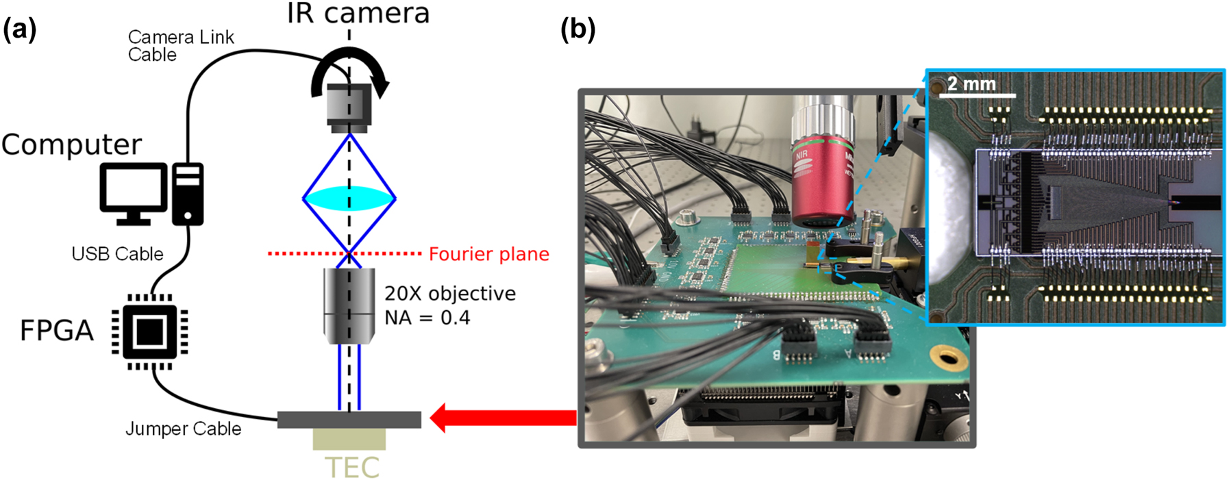
Experimental setup. (a) Schematic of the measurement setup. A rotating Fourier imaging system captures the far-field emission of the packaged OPA chip. The imaging system consists mainly of an infrared camera and a 20× objective lens (NA = 0.4). The hardware specifications are described in the main text. (b) Photograph of a packaged OPA. The PIC is wire-bonded to a printed circuit board with custom driver circuits.
4 Experimental results
In practice, the values of ϵ n (θ, φ) in Eq. (1) are not known apriori. The total error is a combination of effects such as fabrication variation and thermal crosstalk in addition to optical coupling between the waveguide grating antennas [19], [20]. Therefore, we chose an optimization-driven approach to find the set of complex weights {a n } that minimized ϵ n (θ, φ) for different far-field angles. Heuristic optimization algorithms such as the genetic algorithm, particle swarm optimization algorithm, and the gradient descent algorithm are commonly used to calibrate for phase errors in OPAs caused by fabrication variation [21]. To search for solutions of {a n } that would form single-lobe beams, we used a combination of a multi-objective genetic algorithm and a local generalized pattern search algorithm. These algorithms were chosen because they were easy to implement and have previously been applied to array optimization [22], [23], [24].
Both algorithms required feedback on the deviation of the OPA emission pattern from the desired far-field beam pattern. To measure the far-field emission of the OPA, we used the rotatable Fourier imaging system shown in Figure 2(a). The Fourier imaging system had a 47° field-of-view (FOV) in both the θ and φ axes. Two figures of merit (FOM) were used to evaluate the far-field emission in response to a configured {a n }-the sidelobe suppression (SLL) and the integrated power (IP) in a region of interest surrounding the location of the desired beam [24].
Figure 3(a) shows beams formed after optimizing for nine different angles in φ at a constant λ = 1450 nm. The OPA emission before optimization is shown in the top inset of Figure 3(b). Example training curves for the optimization procedures, which are described in more detail in the Appendix, are shown in Figure 3(c) and (d). The images in Figure 3(a) were captured with the imaging system tilted at different angles of φ and stitched together to measure a wider FOV. Beam-steering was achievable up to 110° in φ. For wide-angle characterization of the OPA, λ = 1450 nm was selected because it resulted in near-normal emission (θ ≈ −6°) so that the Fourier imaging system could rotate along φ while remaining fixed at θ = 0°. However, given that small rotations of the imaging system in θ were inevitable, the cross-sectional cuts in Figure 3(b) were taken along an elliptical arc to account for rotations in θ as described in [7].
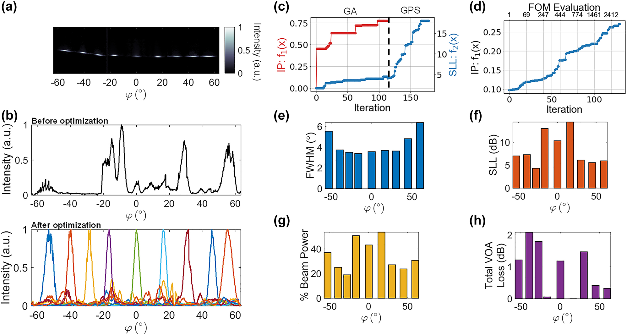
Measurement results for 9 steering angles. (a) Superimposed far-field images for different optimized angles in φ-axis. Each beam is normalized to its maximum intensity (b) Top: OPA emission before optimization. Bottom: Elliptical line cuts of the optimized solutions shown in (a). (c) Figures of merit (FOM) at each iteration for forming a beam at 0° without prior knowledge of existing beam solutions. A multi-objective genetic algorithm (GA) with a population size of 50 and a generalized pattern search algorithm (GPS) were used for the optimization. (d) FOM at each iteration for forming a beam at 55° with the benefit of knowing the optimized values for a solution at 50°. Only the pattern search algorithm was used for the optimization. For the various optimized angles measured: (e) FWHM, (f) sidelobe levels (g) % beam power: power in the main beam as a percentage of the total radiated power (h) total VOA loss: total radiated power normalized to the maximum observed radiated power across all measurements.
Figure 3(e)–(h) plot the full-width at half-maximum (FWHM) beam width, sidelobe level (SLL), percentage of power in the main lobe, and total estimated VOA loss for each of the optimized beam profiles. The FWHM beam widths shown in Figure 3(e), which were approximately 3.6° between [φ min, φ max] = [−30°, 30°], were limited by the aperture size of the array. The SLL (Figure 3(f)) is a ratio of the maximum intensity in the main lobe to the maximum peak intensity outside the lobe in a 2D region defined by [θ min, θ max] = [−23.6°, 23.6°] and [φ min, φ max] = [−63.6°, 63.6°]. The power in the main lobe (Figure 3(g)) is the ratio of the integrated pixel intensity in the direction of the beam between the first nulls to the total pixel intensity in the aforementioned 2D region. Finally, the total VOA loss (Figure 3(h)) is the integrated intensity over all pixels in the 2D region normalized to the maximum total observed across all beam solutions; effectively estimating VOA loss relative to the highest power recorded within the FOV.
For all measurements, image enhancements from the infrared camera (Sensors Unlimited Inc. SU640CSX) were turned off to ensure that the pixel intensity scaled linearly with the input power. The best-optimized solution had an SLL of 14.5 dB and more than 50 % of the total power emitted in the main lobe. The other optimized solutions were limited by the emission characteristics of a single grating antenna, as depicted in Figure 1(d). For example, attempts to direct a beam at an angle of φ = −30° resulted in a low SLL of less than 5 dB and a beam-forming efficiency under 20 %. At this specific angle, the grating emits minimal power, which prevents the formation of a high-quality beam. Furthermore, the grating does not emit substantial power at angles
Figure 4(a) shows the optimized beam profile for φ = 0° compared to the theoretical sinc2 diffraction pattern of a uniformly illuminated rectangular aperture with 32 emitters at a pitch of 775 nm. The two beam profiles show a high degree of similarity, demonstrating successful control over the crosstalk in the emitter aperture. In Figure 4(b), we investigate the robustness of two of the optimized solutions by switching between two sets of optimized coefficients, {a n }, for φ = 0° and φ = 12.5° fifteen times. These consecutive trials are plotted on the same figure and demonstrate that the OPA can be programmed to repeatedly form a beam at the same location with a precision of 0.15°, the resolution of the Fourier imaging system. The standard deviation of the FWHM beam widths was 0.05°. Finally, the near-field emission over the first 250 µm of the emitter aperture, depicted in Figure 4(c), revealed a persistent near-Gaussian power distribution along the grating axis. Adopting a Gaussian distribution is an effective method for sidelobe suppression in an OPA [25]. This similarity demonstrates crosstalk compensation and also suggests that the optimization process approached a near-optimal solution, in alignment with SLL being a figure of merit.
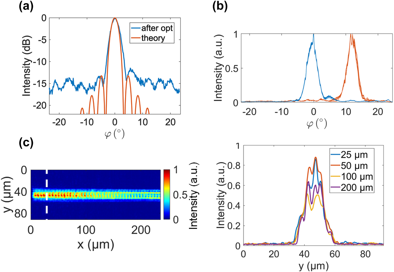
Analysis of measurement results. (a) Comparison of beam formed at 0° with diffraction pattern of a uniformly illuminated rectangular aperture. (b) Fifteen consecutive trials in which the OPA was alternately programmed using two sets of optimized coefficients, {a n } for φ = 0° and φ = 12.5°. (c) Left: Captured near-field emission of the OPA when the beam is steered to 0° in φ. Right: Vertical line cuts of the top image after propagating different distances along the grating axis. The line cuts show a persistent near-Gaussian power distribution.
In Figure 5, we used a combination of wavelength and phase tuning to achieve simultaneous steering in both the θ and φ directions. We traced an oblique line in the far field, by repeating the optimization process at different wavelengths and for different values of φ. By varying the wavelength from 1450 to 1600 nm, we demonstrated beam-steering over 28° from −6° to −34° in the θ-axis. The average beam divergence in θ (Figure 5) was 0.4°. Beam-steering in this dimension was not limited by the wavelength-dependent losses of the components in the fabricated OPA, but limited by the ability to rotate the imaging system along θ beyond −16°. Measurements of test structure components showed that the input wavelength of the designed OPA can be tuned from 1450 to 1650 nm.
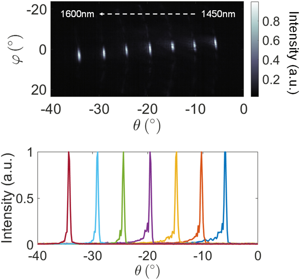
Demonstration of 2D beam-steering. Top: Superimposed far-field images for different optimized angles in φ-axis and θ-axis. To steer in θ, the wavelength is tuned from 1450 to 1600 nm. Bottom: Line cuts in θ of the beams in the image above.
5 Discussion
A limitation of our heuristic optimization approach is the long convergence time needed to find an optimal {a
n
} for beam-forming. For example, without prior knowledge of an optimized {a
n
}, in Figure 3(c) the genetic algorithm required 110 iterations to converge to a solution with approximately 50 FOM evaluations per iteration. This procedure lasted between 10 and 12 hours using the setup in Figure 2 and described in 3.2. The optimization time can be reduced to several hours when the target beam is located within
One evaluation of the FOM- from assigning PWM values on a PC to acquiring and analyzing a far-field image- took a total of 3 s. This time duration was constrained by the data transfer time between the FPGA and the PWM generator registers. The FPGA managed the transfer of incoming USB data to the PWM generator registers via the Advanced eXtensible Interface (AXI) bus, which allowed for updates of the 64 TiN heaters through file writes from a PC. However, data transfer through the AXI bus was performed sequentially, which created a major performance bottleneck. Using AXI Direct Memory Acess (DMA) for parallel data transfers would mitigate this bottleneck, enhancing the system’s performance and its capability to efficiently scale with an increased number of channels in the array.
The optimization algorithms also contributed to inefficiencies in the total optimization time. Specifically, the genetic algorithm often failed to find a global optimum, as illustrated in Figure 3(c), whereas the pattern search algorithm typically showed a gradual progression towards the optimal solution as seen in Figure 3(d). Both algorithms required many iterations because they were iteratively searching a high-dimensional space. For example, with 64 thermo-optic phase shifters, each with approximately 212.5 possible values, there were
Table 1 offers a comparison between the OPA circuit in this work and state-of-the-art OPAs that have demonstrated wide-angle beam-steering
Comparison of various OPA architectures for wide-angle beam steering.
| Ref. | λ (nm) | # of emitters | Steering range (°) | % Beam power | Sidelobe suppression [dB] | Beam divergence (°) | Mechanism for wide-angle steering |
|---|---|---|---|---|---|---|---|
| [8] | 1350–1630 | 128 | 140 × 19.4 | 3.7 %/−14.3 dBa | 6.9 | 0.1 × 0.021 | Aperiodic pitch |
| [28] | 1475–1575 | 256 | 140 × 16 | 2.0 %/−17 dBb | 6.0 | 0.051 × 0.016 | Aperiodic pitch |
| [29] | 1540–1630 | 64 | 120 × 13.9 | 11.0 %/−9.6 dBb | 10.0b | 2.72 × 0.052b | Aperiodic pitch |
| [9] | 1550 | 64 | 120 | 72.0 %/−1.42 dB | 11.4 | 1.6 | λ/2-pitch detuned waveguide array |
| [30] | 1550 | 16 | 160 | Not reported | 7.4 | 6.8 | λ/2-pitch detuned waveguide array |
| [15] | 1480–1580 | 64 | 140 × 13.5 | Highc | 19 | 2.1 × 0.08b | λ/2-pitch detuned waveguide array with slab grating |
| This work | 1450–1600 | 32 | 110 × 28 | 34.5 %/−4.6 dB | 8.2 | 3.6 × 0.4 | λ/2-pitch uniform grating array with amplitude/phase control |
-
aThe OPA insertion loss is not included. bEvaluated for 0° solution. cExact number not given.
6 Conclusions
In summary, we have introduced a novel approach of using programmable amplitudes and phases to overcome the crosstalk in a 1D linear optical phased array with grating emitters spaced at approximately
Funding source: Max-Planck-Gesellschaft
Funding source: Natural Sciences and Engineering Research Council of Canada
Award Identifier / Grant number: RGPIN-2018-06491
Acknowledgment
CMC Microsystems supported the fabrication, which used the Advanced Micro Foundry silicon photonic platform. The authors would like to thank the assistance of J. Zhang of CMC Microsystems.
-
Research funding: The research was supported by the Max Planck Society. A.S. and J.K.S.P. are grateful for funding support from the Natural Sciences and Engineering Research Council of Canada (RGPIN-2018-06491).
-
Author contributions: All authors have accepted responsibility for the entire content of this manuscript and approved its submission.
-
Conflict of interest: Authors state no conflict of interest.
-
Data availability: The datasets generated during and/or analyzed during the current study are available from the corresponding author on request.
A Optimization procedure
Without prior knowledge of an optimized {a n }, to find an initial solution at a given wavelength, we used a genetic algorithm adopted from [24], which optimized the figure of merit,
where f 1(x) is the SLL and f 2(x) is the integrated power (IP) in a region of interest (ROI) surrounding the location of a desired beam. In our work, x is a vector of 64 decision variables representing the programmable amplitudes and phases in the PIC. We evaluated SLL and IP using
Here, ROI denotes the specified region of interest surrounding the desired beam, and I(θ, φ) is the measured far-field intensity at the angles [θ, φ]. For the implementation of the genetic algorithm, we set the population size to 50. After applying the genetic algorithm, we optimized the solution again locally using the generalized pattern search (GPS) algorithm, which is described in [22].
After generating an initial beam, because steering should be continuous, we anticipated that {a
n
} for additional beams near the first solution could be solved using local instead of global optimization. Therefore, subsequent solutions of {a
n
} for different target beams located within
References
[1] N. C. Harris, et al.., “Linear programmable nanophotonic processors,” Optica, vol. 5, no. 12, p. 1623, 2018. https://doi.org/10.1364/optica.5.001623.Search in Google Scholar
[2] D. A. B. Miller, “Perfect optics with imperfect components,” Optica, vol. 2, no. 8, p. 747, 2015. https://doi.org/10.1364/optica.2.000747.Search in Google Scholar
[3] Y. Shen, et al.., “Deep learning with coherent nanophotonic circuits,” Nat. Photonics, vol. 11, no. 7, pp. 441–446, 2017. https://doi.org/10.1038/nphoton.2017.93.Search in Google Scholar
[4] W. Bogaerts, et al.., “Programmable photonic circuits,” Nature, vol. 586, no. 7828, pp. 207–216, 2020. https://doi.org/10.1038/s41586-020-2764-0.Search in Google Scholar PubMed
[5] M. J. R. Heck, “Highly integrated optical phased arrays: photonic integrated circuits for optical beam shaping and beam steering,” Nanophotonics, vol. 6, no. 1, pp. 93–107, 2016. https://doi.org/10.1515/nanoph-2015-0152.Search in Google Scholar
[6] T. Komljenovic, R. Helkey, L. Coldren, and J. E. Bowers, “Sparse aperiodic arrays for optical beam forming and LIDAR,” Opt. Express, vol. 25, no. 3, p. 2511, 2017. https://doi.org/10.1364/oe.25.002511.Search in Google Scholar PubMed
[7] D. N. Hutchison, et al.., “High-resolution aliasing-free optical beam steering,” Optica, vol. 3, no. 8, p. 887, 2016. https://doi.org/10.1364/optica.3.000887.Search in Google Scholar
[8] Y. Li, et al.., “Wide-steering-angle high-resolution optical phased array,” Photonics Res., vol. 9, no. 12, p. 2511, 2021. https://doi.org/10.1364/prj.437846.Search in Google Scholar
[9] C. T. Phare, M. C. Shin, J. Sharma, S. Ahasan, H. Krishnaswamy, and M. Lipson, “Silicon optical phased array with grating lobe-free beam formation over 180 degree field of view,” in Conference on Lasers and Electro-Optics, 2018.10.1364/CLEO_SI.2018.SM3I.2Search in Google Scholar
[10] M. R. Kossey, C. Rizk, and A. C. Foster, “End-fire silicon optical phased array with half-wavelength spacing,” APL Photonics, vol. 3, no. 1, p. 011301, 2017. https://doi.org/10.1063/1.5000741.Search in Google Scholar
[11] L.-M. Leng, Y. Shao, P.-Y. Zhao, G.-F. Tao, S.-N. Zhu, and W. Jiang, “Waveguide superlattice-based optical phased array,” Phys. Rev. Appl., vol. 15, no. 1, p. 014019, 2021. https://doi.org/10.1103/physrevapplied.15.014019.Search in Google Scholar
[12] A. Khavasi, L. Chrostowski, Z. Lu, and R. Bojko, “Significant crosstalk reduction using all-dielectric CMOS-compatible metamaterials,” IEEE Photonics Technol. Lett., vol. 28, no. 24, pp. 2787–2790, 2016. https://doi.org/10.1109/lpt.2016.2623349.Search in Google Scholar
[13] D. Kwong, et al.., “Corrugated waveguide-based optical phased array with crosstalk suppression,” IEEE Photonics Technol. Lett., vol. 26, no. 10, pp. 991–994, 2014. https://doi.org/10.1109/lpt.2014.2311454.Search in Google Scholar
[14] L. Wang, et al.., “Design of a low-crosstalk half-wavelength pitch nano-structured silicon waveguide array,” Opt. Lett., vol. 44, no. 13, p. 3266, 2019. https://doi.org/10.1364/ol.44.003266.Search in Google Scholar PubMed
[15] Y. Liu and H. Hu, “Silicon optical phased array with a 180-degree field of view for 2D optical beam steering,” Optica, vol. 9, no. 8, p. 903, 2022. https://doi.org/10.1364/optica.458642.Search in Google Scholar
[16] H. Steyskal and J. S. Herd, “Mutual coupling compensation in small array antennas,” IEEE Trans. Antennas Propag., vol. 38, no. 12, pp. 1971–1975, 1990. https://doi.org/10.1109/8.60990.Search in Google Scholar
[17] CMC Microsystems, AMF Silicon Photonics General-Purpose Fabrication Process, CMC Microsystems [Online]. Available at: https://www.cmc.ca/amf-silicon-photonics-general-purpose/ Accessed: Nov. 17, 2023.Search in Google Scholar
[18] H. Matsuura, et al.., “Accelerating switching speed of thermo-optic MZI silicon-photonic switches with ‘turbo pulse’ in PWM control,” in 2017 Optical Fiber Communications Conference and Exhibition (OFC), 2017, pp. 1–3.10.1364/OFC.2017.W4E.3Search in Google Scholar
[19] Z. Zhang, M. Notaros, Z. Gao, U. Chakraborty, J. Notaros, and D. S. Boning, “Impact of process variations on splitter-tree-based integrated optical phased arrays,” Opt. Express, vol. 31, no. 8, p. 12912, 2023. https://doi.org/10.1364/oe.487096.Search in Google Scholar PubMed
[20] B. V. Gurses, R. Fatemi, A. Khachaturian, and A. Hajimiri, “Large-scale crosstalk-corrected thermo-optic phase shifter arrays in silicon photonics,” IEEE J. Sel. Top. Quantum Electron., vol. 28, no. 6, pp. 1–9, 2022. https://doi.org/10.1109/jstqe.2022.3189965.Search in Google Scholar
[21] L. Leng, et al.., “Phase calibration for integrated optical phased arrays using artificial neural network with resolved phase ambiguity,” Photonics Res., vol. 10, no. 2, pp. 347–356, 2022. https://doi.org/10.1364/prj.435766.Search in Google Scholar
[22] S. Ebadi, K. Forouraghi, and S. A. Sattarzadeh, “Optimum low sidelobe level phased array antenna design using pattern search algorithms,” in 2005 IEEE Antennas and Propagation Society International Symposium, 2015, pp. 770–773.10.1109/APS.2005.1551677Search in Google Scholar
[23] S. Ebadi and K. Forooraghi, “Pattern scanning in low sidelobe phased array antennas using pattern search algorithms,” in 2007 European Radar Conference, 2007, pp. 347–349.10.1109/EURAD.2007.4405008Search in Google Scholar
[24] Q. Liu, et al.., “Silicon optical phased array side lobe suppression based on an improved genetic algorithm,” in 2020 Asia Communications and Photonics Conference (ACP) and International Conference on Information Photonics and Optical Communications (IPOC), 2020, pp. 1–3.10.1364/ACPC.2020.T2D.3Search in Google Scholar
[25] H. Qiu, Y. Liu, X. Meng, X. Guan, Y. Ding, and H. Hu, “Bidirectional high sidelobe suppression silicon optical phased array,” Photonics Res., vol. 11, no. 4, p. 659, 2023. https://doi.org/10.1364/prj.479880.Search in Google Scholar
[26] S. Bandyopadhyay, R. Hamerly, and D. Englund, “Hardware error correction for programmable photonics,” Optica, vol. 8, no. 10, p. 1247, 2021. https://doi.org/10.1364/optica.424052.Search in Google Scholar
[27] H. Qiu, et al.., “Energy-efficient thermo-optic silicon phase shifter with well-balanced overall performance,” Opt. Lett., vol. 45, no. 17, p. 4806, 2020. https://doi.org/10.1364/ol.400230.Search in Google Scholar
[28] W. Xu, et al.., “Fully integrated solid-state LiDAR transmitter on a multi-layer silicon-nitride-on-silicon photonic platform,” J. Lightwave Technol., vol. 41, no. 3, pp. 832–840, 2023. https://doi.org/10.1109/jlt.2022.3204096.Search in Google Scholar
[29] M. Ye, et al.., “Large steering range and low-loss integrated optical phased array with SiN-Si dual-layer non-uniform antenna,” Opt. Express, vol. 31, no. 26, p. 44564, 2023. https://doi.org/10.1364/oe.507381.Search in Google Scholar PubMed
[30] Y. Kim, H. Yoon, J.-B. You, M. Kim, and H.-H. Park, “Wide-angle beam-steering using an optical phased array with non-uniform-width waveguide radiators,” Photonics, vol. 7, no. 3, p. 56, 2020. https://doi.org/10.3390/photonics7030056.Search in Google Scholar
Supplementary Material
This article contains supplementary material (https://doi.org/10.1515/nanoph-2023-0819).
© 2024 the author(s), published by De Gruyter, Berlin/Boston
This work is licensed under the Creative Commons Attribution 4.0 International License.
Articles in the same Issue
- Frontmatter
- Editorial
- Programmable nano-optics and photonics
- Reviews
- Towards large-scale programmable silicon photonic chip for signal processing
- Phase change material-based tunable Fano resonant optical coatings and their applications
- Perspectives
- Melting-free integrated photonic memory with layered polymorphs
- Chalcogenide phase-change material advances programmable terahertz metamaterials: a non-volatile perspective for reconfigurable intelligent surfaces
- Research Articles
- Fundamental limits to multi-functional and tunable nanophotonic response
- Spatio-spectral control of coherent nanophotonics
- Nanoantenna induced liquid crystal alignment for high performance tunable metasurface
- Programmable topological metasurface to modulate spatial and surface waves in real time
- Programmable flip-metasurface with dynamically tunable reflection and broadband undistorted transmission
- High-resolution non-line-of-sight imaging based on liquid crystal planar optical elements
- Ultrafast Q-boosting in semiconductor metasurfaces
- Inverse design of compact nonvolatile reconfigurable silicon photonic devices with phase-change materials
- Integrated multi-operand optical neurons for scalable and hardware-efficient deep learning
- Surface plasmon-cavity hybrid state and its graphene modulation at THz frequencies
- Language-controllable programmable metasurface empowered by large language models
- All optical tunable RF filter using elemental antimony
- Reconfigurable application-specific photonic integrated circuit for solving partial differential equations
- Optimization of a programmable λ/2-pitch optical phased array
- Closed-loop electron-beam-induced spectroscopy and nanofabrication around individual quantum emitters
- High-fidelity and polarization-insensitive universal photonic processors fabricated by femtosecond laser writing
- Direct electron beam patterning of electro-optically active PEDOT:PSS