
High-efficiency broadband light coupling between optical fibers and photonic integrated circuits
-
Gyeongho Son


Abstract
Efficient light energy transfer between optical waveguides has been a critical issue in various areas of photonics and optoelectronics. Especially, the light coupling between optical fibers and integrated waveguide structures provides essential input-output interfaces for photonic integrated circuits (PICs) and plays a crucial role in reliable optical signal transport for a number of applications, such as optical interconnects, optical switching, and integrated quantum optics. Significant efforts have been made to improve light coupling properties, including coupling efficiency, bandwidth, polarization dependence, alignment tolerance, as well as packing density. In this review article, we survey three major light coupling methods between optical fibers and integrated waveguides: end-fire coupling, diffraction grating-based coupling, and adiabatic coupling. Although these waveguide coupling methods are different in terms of their operating principles and physical implementations, they have gradually adopted various nanophotonic structures and techniques to improve the light coupling properties as our understanding to the behavior of light and nano-fabrication technology advances. We compare the pros and cons of each light coupling method and provide an overview of the recent developments in waveguide coupling between optical fibers and integrated photonic circuits.
1 Introduction
Low-loss optical interfaces between different types of optical waveguides are crucial for the efficient and reliable transfer of optical signals in a number of applications, including optical interconnects [1], nonlinear optical signal processing [2], [3], and integrated quantum optics [4]. The optical coupling efficiency between two waveguides is defined by the ratio of guided optical powers before and after the coupling process and can be determined by the waveguide mode overlap condition [5]. Efficient low-loss optical coupling between waveguides made of dissimilar materials is important in providing seamless optical interfaces for heterogeneous photonic integration. Especially, optical coupling between optical fibers and integrated waveguides in the photonic integrated circuits (PICs) and their systems is of growing interest with the recent advances in integrated photonics. Optical fibers have many attractive properties as an optical waveguide, such as low transmission loss, low cost, flexibility, and electromagnetic immunity, and therefore can provide an ideal conduit between various optical components and systems, including PICs [6].
The integration density of optical waveguides in the PIC platform is closely related to the refractive index contrast between the core and the cladding materials. As waveguides based on high-index waveguide core materials with large index contrasts to the cladding have much smaller waveguide dimensions and bending radii, the integration density of such high-index PIC platforms can be significantly increased. As the demand for more compact integrated optical components increases, high refractive index materials, such as silicon [7], [8] and III-V compound semiconductors [9], [10], are required for large-scale high-density PICs. For example, for single-mode operation at telecommunication wavelengths (e.g. 1550 nm), the cross-section of a silicon waveguide (a refractive index of 3.45) embedded in a silica cladding (a refractive index of 1.45) must be on a submicron scale (e.g. 400 nm×220 nm), and the corresponding guided optical mode profile is highly confined in the waveguide core with a typical mode area on the order of 0.1 μm2 [11]. Because of the highly confined optical modes, a tight bending radius of less than 5 μm can be achieved, which results in ultracompact guided optical components while allowing more flexibilities in the photonic circuit layout.
In contrast to the small mode size of the high-index integrated waveguide, the typical mode-field diameters (MFDs) of standard single-mode fiber (SMF) at telecommunication wavelengths are about 10 μm. The difference in the cross-sectional area between those two waveguides is about 1000 times, which poses a great challenge to efficient optical coupling. For comparison, fiber-to-PIC interfaces for silica-based planar lightwave circuits [12], [13], [14] can achieve very high coupling efficiencies of up to −0.05 dB (98.9%) [14] mainly because the integrated waveguides and optical fibers are made of the similar silica materials with low-index contrasts and they have similar waveguiding properties, such as mode profile and effective modal index.
Significant efforts have been made to improve various aspects of fiber-to-PIC light coupling, and the important figures of merit (FOMs) include coupling efficiency, operating wavelength range or bandwidth, polarization sensitivity, misalignment tolerance, and scalability. In this article, we review three important classes of optical coupling schemes between optical fibers and integrated waveguides based on high refractive index materials, such as silicon, in the near-infrared wavelength range and compare their performances based on the FOMs. In our classification, the three major fiber-to-PIC light coupling methods are end-fire coupling, diffraction grating-based coupling, and adiabatic coupling.
The end-fire coupling methods have been mainly used for low-port-count photonic chip packaging. Although end-fire coupling provides broadband and polarization-insensitive optical coupling properties, it typically requires precise alignment tolerances on the order of ±0.5 μm for 1-dB excess optical losses [15]. Recent progress and notable achievements in end-fire coupling are reviewed in Section 2.
In Section 3, we review diffraction grating-based optical coupling. Grating coupling has three representative advantages compared to end-fire coupling: post-processing, such as dicing or polishing, is not required, which allows in-process wafer-scale optical characterization and testing; the coupler structures do not need to be located at the chip edges, which improves layout design flexibility and optical port scalability; and alleviated alignment tolerance makes measurement and packaging processes simpler. The grating-based couplers are, however, polarization- and wavelength-dependent and show relatively low coupling efficiencies when compared to the end-fire couplers.
Adiabatic coupling seems similar to end-fiber coupling but is based on evanescent power transfer through waveguide tapers and can achieve very high coupling efficiency, broadband coupling, and compact coupler footprint. Recent progresses in this method are reviewed in Section 4.
2 End-fire coupling
Because of its physical proximity between optical waveguides’ end facets, end-fire coupling (also referred to as butt coupling or edge coupling) is considered as the most straightforward way to connect two different waveguides and transfer optical signals between them. End-fire coupling between the optical fiber and the integrated waveguide for the chip-scale PIC platform has therefore been a well-established approach for relatively low port count connections, and examples include fiber-pig-tailing for semiconductor laser chips [16], [17], [18], input and output fiber connection for optical waveguide-based modulators [19], and optical switches [20], [21]. Figure 1A and B show a schematic diagram of single-mode fiber-to-laser chip coupling and an example of a packaged device, respectively [18]. Although it is possible to use lenses and other discrete optical components between the fiber and the PIC chip to improve the optical coupling characteristics, we mainly focus on the direct end-fire coupling schemes without bulk optics in this review. In 1977, Hunsperger et al. [17] adopted an end-fire coupling method to directly couple the light output from a GaAs semiconductor laser to a Ta2O5 waveguide without an intermediate optical fiber. Burns et al. [22] and other researchers [23], [24] also introduced end-fire coupling schemes between optical fibers and LiNbO3 (or LiTaO3) diffused channel waveguides. End-fire coupling methods for InP/InGaAsP waveguides [25], [26], [27], GaAs/AlGaAs waveguides [28], [29], [30], and photodiodes [31], [32] with low wavelength and polarization dependencies were also developed. By using a tapered waveguide structure (larger waveguide dimensions toward the terminating end), the end-fire optical coupling techniques with the diffused channel waveguides exhibited low optical insertion losses less than 1 dB [25]. Researchers have also employed tapered waveguide structures with larger facet sizes [23], [26], [27] to extend the effective optical mode diameter, up to the order of 10 μm, and efficiently coupled the light signal to the glass optical fibers with similar MFDs. These approaches also show small wavelength- and polarization-dependent losses of less than 1 dB.
![Figure 1: Conventional coupling schemes for semiconductor lasers.(A) Schematic diagram of end-fire coupling for fiber-to-laser connection. (B) An example of a packaged single-mode coupler. Reprinted from Ref. [18]. Copyright (1980) The Optical Society.](/document/doi/10.1515/nanoph-2018-0075/asset/graphic/j_nanoph-2018-0075_fig_001.jpg)
Conventional coupling schemes for semiconductor lasers.
(A) Schematic diagram of end-fire coupling for fiber-to-laser connection. (B) An example of a packaged single-mode coupler. Reprinted from Ref. [18]. Copyright (1980) The Optical Society.
In this section, we start our discussion by introducing the operating principle of end-fire coupling in Section 2.1. Notable research achievements with tapered waveguide structures are reviewed in Section 2.2. Enhanced optical coupling schemes with intermediate waveguide regions (Section 2.3) and vertically curved and suspended waveguide structures (Section 2.4) are also reviewed. Table 1 compares the performances of various end-fire coupling schemes according to the major FOMs.
Summary of the reported end-fire coupling methods.
| Organization | Ref. | Year | Fiber | Coupling efficiency (dB) | Operation wavelength (nm) | Facet size (μm×μm) | Comments | |
|---|---|---|---|---|---|---|---|---|
| TE | TM | |||||||
| 2.2 Tapered waveguides | [33] | 2003 | Cleaved SMF | −3.47~−2.22 (−0.86*) | 1550 | 15×10 | Shadow mask sputtering | |
| [34] | 2003 | Cleaved SMF | −0.6 | 1550 | 10×10 | RIE | ||
| [35] | 2007 | Cleaved SMF | −0.5 | N.A. | 1550 | 10×6.6 | Shadow mask sputtering | |
| [36] | 2009 | Cleaved SMF | −0.52 | 1550 | 5.6×5 | ICP etching | ||
| [37] | 2009 | Cleaved SMF | −0.48 | 1550 | 6×6 | 3D silicon taper | ||
| 2.3 Enhanced optical coupling with intermediate waveguide regions | [38] | 2002 | Cleaved SMF | −3.5 | 1560 | 3×3 | Polymer cladding | |
| [39] | 2010 | Cleaved SMF | −0.66 | −0.36 | 1480–1550 | 3.4×3.4 | Oxidation-silicon width decreases | |
| [40] | 2013 | Cleaved SMF | −4.2 | −3.6 | 1550 | 10×8 | SU8 outer waveguide | |
| [41] | 2010 | Cleaved SMF | −0.7 | −0.8 | 1570 | 6×4 | Suspension, SiO2 outer waveguide | |
| [42] | 2018 | Cleaved SMF | −0.95 | −1.3 | 1550 | 10×4 | Suspension, SiO2 outer waveguide | |
| 2.4 Vertically curved and suspended waveguide structures | [43] | 2012 | Tapered fiber | −0.62 | −0.5 | 1550 | 2×2.1 | Annealing bent, SiO2 outer waveguide |
| [44] | 2016 | Lensed fiber | −2.2 | −3.6 | 1550 | 0.42×0.22 | Implantation bent | |
The coupling efficiencies with “*” indicate the simulated results.
2.1 Principle of operation
Figure 2A schematically (not drawn to scale) shows a typical end-fire coupling scenario between two waveguides with an arbitrary intermediate coupling region. In this review article, we are mostly interested in passive optical coupling between an optical fiber and an integrated waveguide and assume that the input optical power from the input waveguide (waveguide 1 in Figure 2A, e.g. a silica-based single-mode optical fiber) is carried by a guided optical mode, whose field profile is given by E1. In this analysis, we pay our attention only to a specific input mode E1, but the same analysis can be applied to other input modes that are orthogonal to E1. We further assume that the output waveguide (waveguide 2 in Figure 2A, e.g. a silicon waveguide) can support multiple guided modes, and the field profile for the kth mode is given by E2,k. Optical coupling efficiencies between two guided modes, E1 and E2,k, can be defined using the optical power ratio as (neff,2,k/neff,1)·|E2,k |2/|E1|2. Because of the reciprocity theorem, the coupling properties are bidirectional, and the coupling efficiency remains the same when the role of input and output is reversed.
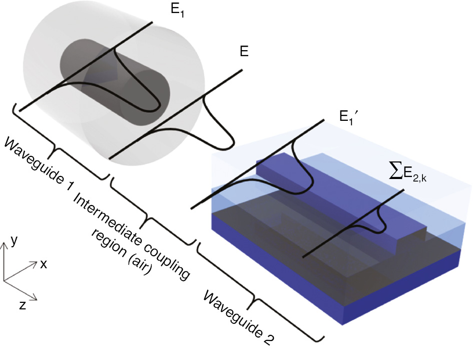
Schematic diagram of the end-fire coupling process between two waveguides.
The input guided mode in the waveguide 1 (E1, for example, the HE11 mode in the SMF); incoming electromagnetic field after passing through the intermediate coupling region (E1′); output guided modes in the waveguide 2 (∑E2,k). Non-coupled radiation modes (Eβ) are not shown.
The guided mode of the input waveguide (E1) is first radiated through the intermediate coupling region after partial reflection and transmission (with a transmission coefficient of t1) at the end facets of the waveguide. The radiated optical field (E) propagates through the intermediate coupling region and arrives at the front facet of the waveguide 2. The optical field measured in front of the waveguide facet is given by E1′, which can be finally coupled to the output guided modes ∑E2,k. The coupling efficiency between E1′ and E2,k can be quantitatively obtained from the overlap integral (η) and the transmittance (|t2|2). Partial reflections may occur at the interfaces due to the differences in the effective refractive indices, and the corresponding transmission coefficient is given by t2=2(neff,1′×neff,2,k)0.5/(neff,1′+neff,2,k), where neff,1′ is the effective refractive index for the intermediate coupling region and neff,2,k is the effective modal index for the kth guided mode in the output waveguide.
A typical single-mode optical fiber has only one guided mode (fundamental HE11 mode) when considering only one polarization state. The incoming electric field (E1′) can be decomposed into the linear combination of the orthogonal guided modes (E2,k) of the output waveguide and the non-guided modes (Eβ) and is given by [45] the following:
where the expansion coefficient ck can be obtained using the Poynting theorem and is given by the following:
The overlap integral between the incoming field (E1′) and the kth guided mode is given by the following:
The overlap integral in Equation 2.3 represents the similarity of the optical field profiles between E1′ and E2,k. In addition to the field overlap, we need to take into account the partial optical reflections at the interface, resulting from the abrupt changes in the effective refractive index. Therefore, the total optical power coupling efficiency from the incoming field E1′ into the kth guided mode for the output waveguide (E2,k) is finally given by |t2|2·ηk. The optical power transfer efficiency from the input waveguide mode (E1) to the field profile in front of the output waveguide (E1′) can be similarly obtained as described above. When the intermediate coupling region consists of, for example, free-space, the radiated beam from the input waveguide 1 (e.g. silica-based optical fiber) diverges with a numerical aperture (NA) determined by the core (ncore) and cladding (ncladding) indices [NA=(ncore2 ‒ ncladding2)1/2], and the full divergence angle is 2θ0=4λ/(2×π×W0), where W0 is the beam waist radius. The detailed electric field profile with respect to the propagation distance from the waveguide end facet can be obtained from the diffraction theory. Because of rapid beam divergence, when the distance between the waveguides is too far, the incident beam profile (E1′) shows a low overlap integral value with E2,k and results in a low coupling efficiency to a specific output mode. We also need to consider partial reflections at the interfaces between waveguide 1 and the intermediate coupling region (E1 and E) and between the intermediate coupling region and waveguide 2 (E1′ and ∑E2,k) due to the different effective indices in each region.
There exist various strategies to improve the overall optical coupling efficiencies. For example, three-dimensional tapered waveguide structures can be used to mitigate the MFD mismatches between the input and output waveguides (E1 and E2,k) and thereby increase the overlap integral values (ηk). Another way to improve the coupling efficiency is by lowering the partial reflections at the interfaces (increasing t1 and t2) with intermediate index regions, such as oxide and polymer layers instead of air, due to the reduced effective index contrast. In addition to using the lower index material in the intermediate coupling region, the waveguide itself can be inversely tapered (sharper waveguide tip) to provide gradual transformation of the effective index as well as to obtain lower effective modal index toward the transition region.
2.2 Tapered waveguides
Lateral [46], [47], vertical [48], and three-dimensional [49], [50] waveguide taper designs have been introduced to enlarge the effective MFD of the integrated waveguides with high-index core materials (e.g. III–V compound semiconductor and silicon). These types of intermediate coupling structures are also referred to as spot-size converters (SSCs or mode-size converters) [51] and gradually increase the width and/or height of the integrated waveguide to provide a large terminating facet area up to 100 μm2, which is close to that of the fiber core, as schematically shown in Figure 3A. The tapering angle of the SSC transition region needs to be carefully designed to prevent unwanted light coupling to the higher order modes for the tapered waveguide region. An extended waveguide facet dimension through the SSC can achieve an enlarged electromagnetic field profile, resulting in a higher mode overlap value (η), as described in Section 2.1.
![Figure 3: (A) Schematic diagram of a three-dimensionally tapered intermediate waveguide structure. (B) An example of a vertically tapered waveguide fabricated by gray-tone shadow masking.Adapted from Ref. [35], Copyright 2007 American Institute of Physics.](/document/doi/10.1515/nanoph-2018-0075/asset/graphic/j_nanoph-2018-0075_fig_003.jpg)
(A) Schematic diagram of a three-dimensionally tapered intermediate waveguide structure. (B) An example of a vertically tapered waveguide fabricated by gray-tone shadow masking.
Adapted from Ref. [35], Copyright 2007 American Institute of Physics.
Three-dimensionally tapered SSCs have been employed in the silicon-based PIC platform for efficient optical coupling between optical fibers and integrated silicon waveguides [33], [34], [35], [36], [37], [52], [53]. Such SSC structures can be fabricated with conventional silicon waveguides on silicon-on-insulator (SOI) wafers using additional fabrication processing steps, such as polishing [52], etching [34], [36], [37], [53], and gray-tone shadow masking [33], [35], [54]. As shown in a scanning electron microscope (SEM) in Figure 3B, Shiraishi et al. used a metal shadow mask fabrication process [54] to make a vertical waveguide taper [35]. Starting from the silicon waveguide cross-section of 500 nm in height and 300 nm in width, a total taper length of 2 mm and a final waveguide width of 10 μm were achieved with a linear taper. The final waveguide width is close to the standard single-mode fiber MFD. Amorphous hydrated silicon (a-Si:H) was deposited to extend the vertical mode dimensions in the laterally extended silicon waveguide. A measured net transmission loss of 0.5 dB was obtained at the input wavelength of 1.55 μm using a lensed fiber.
Although this type of guided mode expansion approaches offers good coupling efficiency of better than −1 dB and seems straightforward in concept, it requires additional dedicated fabrication steps, such as thick materials deposition and etching. It might also occupy more space when compared to other coupling schemes.
2.3 Enhanced optical coupling with intermediate waveguide regions
Optical mode profiles and their cross-sectional areas can be extended not only by expanding the waveguide dimensions with waveguide tapers as discussed in the previous section but also by shrinking the waveguide dimensions, as schematically shown in Figure 4A. When the waveguide cladding material has an intermediate refractive index (larger than air but smaller than the waveguide core refractive index) and thus provide a smaller index contrast, the optical modes are less confined to the waveguide core as the core dimensions decrease, resulting in larger effective mode areas and smaller effective modal index. The low-index intermediate cladding layers, such as polymer [38], [39], [56], [57], [58], SiO2 [55], [59], [60], [61], [62], and Si3N4 or SiON [40], [62], [63] with effective refractive indices comparable to optical fibers, can efficiently expand the optical mode dimensions and reduce the partial reflections at the interfaces [38], [39], [40], [55], [56], [57], [58], [59], [60], [61], [62], [63]. The input light gets adiabatically expanded through the inversely tapered high-index waveguide and can be finally coupled to the optical fiber with a high coupling efficiency.
![Figure 4: (A) Schematic diagram of an inversely tapered intermediate waveguide coupler with a low-index cladding. The integrated waveguide core region is represented with blue colors. (B) A typical inversely tapered waveguide coupler with SiO2 cladding layers. Reprinted from Ref. [55]. Copyright 2003 The Optical Society. (C) A coupler with a very narrow tip fabricated by silicon oxidation process and its SEM image. Silicon nano-taper tip end (I) before and (II) after oxidation process. (III) Top view of the junction point of a polymer core and a silicon waveguide. (IV) Cross-section view of the nano-taper coupler.Adapted from Ref. [39]. Copyright 2010 Elsevier.](/document/doi/10.1515/nanoph-2018-0075/asset/graphic/j_nanoph-2018-0075_fig_004.jpg)
(A) Schematic diagram of an inversely tapered intermediate waveguide coupler with a low-index cladding. The integrated waveguide core region is represented with blue colors. (B) A typical inversely tapered waveguide coupler with SiO2 cladding layers. Reprinted from Ref. [55]. Copyright 2003 The Optical Society. (C) A coupler with a very narrow tip fabricated by silicon oxidation process and its SEM image. Silicon nano-taper tip end (I) before and (II) after oxidation process. (III) Top view of the junction point of a polymer core and a silicon waveguide. (IV) Cross-section view of the nano-taper coupler.
Adapted from Ref. [39]. Copyright 2010 Elsevier.
Figure 4B shows an example of an inversely tapered waveguide coupler, which transforms both the effective mode size and effective mode index between an optical fiber and an integrated silicon waveguide [55]. The inversely tapered silicon waveguide (smaller waveguide dimensions toward the terminating end) has a tapering length of ~40 μm, and the waveguide width reduces from ~470 nm (single-mode waveguiding condition) to ~100 nm with a waveguide height of 270 nm. Due to the expanded mode size at the subwavelength-scale waveguide tip, the maximum mode overlap with an input lensed fiber (MFD=~5 μm) was calculated to be as high as 94%, and this corresponds to a mode mismatch loss of 0.26 dB. The total insertion losses with partial reflections and misalignment were measured to be ~3.3 dB and 6.0 dB for the TM (an effective refractive index of 1.51) and TE (an effective refractive index of 1.31) modes, respectively [55]. Although there is a large index contrast between the silicon core material and the SiO2 cladding layer, the propagating electromagnetic field for the very narrow inversely tapered waveguide structure resides mostly outside the core region and its effective modal index becomes close to the refractive index of the SiO2 cladding layer.
Using a similar approach with a combination of an intermediate polymer region and a SiO2 cladding layer, Pu et al. reported very low optical coupling losses of ~0.36 dB and ~0.66 dB for the TM and TE modes, respectively [39] (Figure 4C). The ultra-low losses were obtained using a very narrow silicon taper tip whose width was reduced from ~40 nm to ~12 nm by silicon oxidation.
To further improve the fiber-to-chip optical coupling efficiency with intermediate waveguide structures, suspended waveguide structures with low-index cladding materials, such as SiO2 [41], [42], [64], [65], [66] and SiON, were investigated [67], as schematically shown in Figure 5A. Figure 5A shows a tapered silicon waveguide, surrounded by a SiO2 cladding cantilever structure, is suspended [65]. After formation of the tapered silicon waveguide and SiO2 cladding cantilever structure (13 μm×10 μm), the underlying Si substrate was etched to form a trench, as shown in Figure 5A. The optical power leakage to the substrate was minimized by providing a sufficiently large trench depth. The coupling efficiencies were measured to be −1.5 dB and −1.0 dB for the TM and TE modes, respectively. As the suspended waveguide structures have an alignment tolerance of approximately ±2.0 μm for a 1-dB excess loss, which is better than other end-fire coupling schemes, it may have benefits in the fiber assembly and packaging processes [42], [65]. Multi-layered suspended tapering structures can further improve the coupling efficiencies by gradually transforming the effective refractive index between high-index silicon waveguides and low-index optical fibers [62], [64], [65], [66].
![Figure 5: (A) Schematic diagram of a suspended intermediate waveguide structure. (B) An example of an inversely tapered silicon waveguide surrounded by a SiO2 cladding with a cantilever structure. The SEM images of the fabricated couplers are shown.Adapted from Ref. [65]. Copyright (2011) The Optical Society.](/document/doi/10.1515/nanoph-2018-0075/asset/graphic/j_nanoph-2018-0075_fig_005.jpg)
(A) Schematic diagram of a suspended intermediate waveguide structure. (B) An example of an inversely tapered silicon waveguide surrounded by a SiO2 cladding with a cantilever structure. The SEM images of the fabricated couplers are shown.
Adapted from Ref. [65]. Copyright (2011) The Optical Society.
This type of end-fire coupling with inversely tapered high-index waveguides can achieve efficient optical coupling with small footprints and low wavelength/polarization dependencies. Similar approaches in this category include waveguide ribbon layers [68], [69], [70], photonic wire bonding [71], [72], [73], and free-form lenses and mirrors [74], [75]. Figure 6A and B show examples of single-channel SSC interconnects [69], [70]. Multi-port coupling examples using photonic wire bonds and free-form components are illustrated in Figure 6C [71] and D [74], respectively. Recently, several researchers have exploited subwavelength grating (SWG) converters based on high-index materials, such as silicon [76], [77], [78]. By engineering the effective refractive index of the waveguides, SWG-based end-fire couplings can achieve coupling efficiencies as high as −0.32 dB (93%) [78].
![Figure 6: Optical interfaces for multiple ports using intermediate mode transformation stages.(A) Schematic diagram of a multi-channel SSC interconnecting multiple fibers and waveguide arrays. Reprinted from Ref. [70]. Copyright (2011) The Optical Society/IEEE. (B) Schematic diagram of the polymer interface linking an array of standard SMFs to an array of nanophotonic waveguides. Reprinted from Ref. [69]. Copyright (2014) IEEE. (C) SEM image of a multi-core fiber-to-chip interface using photonic wire bonds to connect the individual cores of the multi-core fiber to an array of silicon waveguides. Reprinted from Ref. [71]. Copyright (2015) The Optical Society/IEEE. (D) Schematic diagram of free-form lenses and expanders. Reprinted from Ref. [74]. Copyright (2018) Nature Publishing Group.](/document/doi/10.1515/nanoph-2018-0075/asset/graphic/j_nanoph-2018-0075_fig_006.jpg)
Optical interfaces for multiple ports using intermediate mode transformation stages.
(A) Schematic diagram of a multi-channel SSC interconnecting multiple fibers and waveguide arrays. Reprinted from Ref. [70]. Copyright (2011) The Optical Society/IEEE. (B) Schematic diagram of the polymer interface linking an array of standard SMFs to an array of nanophotonic waveguides. Reprinted from Ref. [69]. Copyright (2014) IEEE. (C) SEM image of a multi-core fiber-to-chip interface using photonic wire bonds to connect the individual cores of the multi-core fiber to an array of silicon waveguides. Reprinted from Ref. [71]. Copyright (2015) The Optical Society/IEEE. (D) Schematic diagram of free-form lenses and expanders. Reprinted from Ref. [74]. Copyright (2018) Nature Publishing Group.
2.4 Vertically curved and suspended waveguide structures
One of the main disadvantages of the conventional end-fire coupling methods is that the optical interfaces to the input/output fibers need to be located at the PIC chip edges and the dicing process is required to expose the end-fire coupler structures to the optical fibers. However, the out-of-plane light coupling can be achieved by physically bending the waveguides toward the upward direction from which the optical fibers are approached [43], [44], [79], [80], as schematically shown in Figure 7A. While providing the advantages of conventional end-fire coupling, such as low wavelength and polarization dependencies, this out-of-plane coupling scheme does not require the optical couplers to be located at the chip edges.
![Figure 7: (A) Schematic diagram of a vertically curved intermediate waveguide structure. (B) SEM image of a curved coupler using thermal annealing. Reprinted from Ref. [79]. Copyright (2009) The Optical Society. (C) SEM image of a bent waveguide coupler with a radius of curvature of 3 μm using ion implantation.Reprinted from [44]. Copyright (2016) The Optical Society/IEEE.](/document/doi/10.1515/nanoph-2018-0075/asset/graphic/j_nanoph-2018-0075_fig_007.jpg)
(A) Schematic diagram of a vertically curved intermediate waveguide structure. (B) SEM image of a curved coupler using thermal annealing. Reprinted from Ref. [79]. Copyright (2009) The Optical Society. (C) SEM image of a bent waveguide coupler with a radius of curvature of 3 μm using ion implantation.
Reprinted from [44]. Copyright (2016) The Optical Society/IEEE.
The bent waveguide couplers can be fabricated by introducing stress gradients to the waveguide structure so that the waveguide termination region can be bent upward when released from the substrate [81], [82]. The overall footprint for the bent waveguide coupler is closely related with its bending radius. As highly confined optical modes in the high-index waveguides allow small bending radii of less than 10 μm without too much radiation losses occurring, the vertically curved waveguide coupler design can be compact and scalable while providing the benefits of end-fire coupling.
For example, out-of-plane optical coupling to the optical fibers or free-space optical beams was obtained by stress-engineered Si/SiO2 cantilevers deflected upward by thermal annealing stress, as shown in Figure 7B [79]. Tapered silicon waveguides were embedded in the center of the SiO2 cantilevers. After the deposition of PECVD SiO2 layer, the SiO2 cantilevers are released from the substrate by reactive ion etching and subsequently annealed for stress control. Maximum deflection and tilt angles at the end of a 40-μm-long SiO2 cantilever with silicon core in the center are 2.6 μm and 4.7°, respectively. Because of limitations in maximum stress level from the thermal annealing process, the bending radii obtained from this method were limited to approximately 100 μm [79], [83]. To introduce higher stress gradients and thereby reduce the bending radius of the curved waveguide structure for smaller coupler dimensions, an ion beam implantation method was applied to intentionally introduce lattice defects. As a result, a bending radius of approximately 3 μm was obtained, as shown in Figure 7C [44]. The vertically curved waveguide coupler structures showed ~−1 dB (80%) optical coupling efficiencies with tapered fibers [43], [79] and lensed fibers [44], [80].
3 Diffraction grating-based optical coupling
Diffraction grating-based optical coupling methods have been proposed, as an alternative solution to end-fire coupling, to deal with mode size mismatches between optical fibers and integrated waveguides in the PIC platforms as well as to provide scalable optical interfaces from the surface-normal direction instead of chip edges [84]. Surface-corrugated grating structures with subwavelength-scale feature sizes are usually patterned in the PIC’s waveguide layer to create a coherent constructive interference condition that diffractively couples the incident free-space optical beam from the optical fiber into the high-index waveguides, or vice versa. In 2002, Taillaert et al. presented an out-of-plane coupling method for efficient light transfer between the optical fibers and planar waveguides using grating components on a 240-nm-thick GaAs core material with an oxide cladding layer [29]. Because of its out-of-plane coupling geometry, the grating couplers do not need to be located on the chip edges and thus enable wafer-scale PIC characterization capabilities without requiring chip dicing and polishing. The grating couplers have a typical tolerance value of ±2 μm for 1-dB excess losses [85]. This is a relaxed spatial alignment tolerance compared to the end-fire coupling methods.
Initial works on the integrated diffraction grating structures have first focused on manipulation and collimation of free-space optical beams [86], [87], [88] or output light collimation from the laser diodes [89], [90], [91]. Coupling of the laser beam to a thin glass film was experimentally achieved using a periodic grating structure made from photoresists directly fabricated on the glass film [87]. A blazed grating structure was also proposed to enhance the directionality and coupling efficiency [92]. In the 2000s, with the emergence of foundry-based silicon photonics platforms, grating couplers began to be fabricated on SOI wafers and intimately integrated with PICs using batch microfabrication processes, which enabled scalable surface-normal optical interfaces between the optical fibers and PIC platforms [93], [94], [95]. In addition, polarization-diversity grating couplers were implemented by taking advantages of polarization splitters/combiners [96], [97], [98], [99], and a low polarization-dependent loss comparable to the end-fire couplers (<1 dB) was achieved [99]. Since 2010, based on advances in fabrication techniques, the SWG structures have been also exploited in surface coupling methods to improve the coupling efficiencies [100], [101], [102] and obtained polarization-independent operation [103] by engineering the effective refractive indices for different input polarization states. SWG-based couplers can also achieve a wide 3-dB spectral bandwidth of ~117 nm by tailoring the dispersion of the grating structures [104]. Moreover, arrays of grating couplers and fibers, including multi-core fibers, have been introduced to facilitate large-scale packaging and multiple-port parallel device characterization [105], [106], [107], [108].
In this section, the operating principle of diffraction grating-based optical couplers is first introduced in Section 3.1. Figure 8A shows an overall schematic diagram of a typical grating coupler (not drawn to scale). Figure 8B shows its z-y plane cross-sectional view with the directions of the diffracted light components. We consider a simple case where the grating is composed of diffractive elements placed along the waveguide propagation direction. Although the diffraction grating-based coupling schemes can be in principle applied to various materials, we mostly focus on the silicon-based PIC platform in this review article. The efficient fiber-to-chip coupling can be typically achieved using a combination of an adiabatically tapered waveguide region for horizontal mode size conversion and a grating coupler with a ~10-μm width similar to the MFD of typical SMFs at telecommunication wavelengths around 1550 nm [95]. The waveguide taper region connects a single-mode waveguide with a grating coupler and transforms the optical field distribution along the width direction (x-axis in Figures 8 and 9) perpendicular to the waveguide’s propagating axis (z-axis in Figures 8 and 9). The grating elements diffract the guided optical beam out of the waveguide plane, and the diffracted optical beam finally couples to the optical fiber’s guided mode.
Diffraction grating-based optical coupling with uniform grating components.
(A) Schematic diagram of a diffraction grating-based coupling structure. (B) Cross-section view of (A).
Wavevector representation of the Bragg condition for the grating coupler.
(A) Perfectly vertical operation, which generates the second-order diffraction (m=2) with increased back-reflection. (B) Off-normal operation only generating the first-order diffraction (m=1) while reducing back-reflection (black arrow: the propagation constant in the waveguide region; purple arrow: the reciprocal lattice vector of the grating; red arrow: the wavevector of the upward-diffracted wave; green arrow: the wavevector of the downward-diffracted wave).
The coupling efficiency between the obliquely (or sometimes vertically) incident free-space optical beam and the guided light in the integrated waveguide for this basic grating coupler is often limited by two factors. First, some optical losses result from the optical field profile mismatch between the fiber’s propagating mode and the free-space optical beam diffracted upward from the grating coupler. Second, when the light transmitted through the waveguide meets the grating structure, it propagates not only to the upper cladding part but also to the lower substrate, which reduces the overall coupling efficiency toward the optical fiber. To obtain better efficiencies, grating-based coupling methods have employed arrays of apodized diffractive elements, achieving both enhanced directivity and mode overlap. Additional optical feedback structures, such as additional backside mirrors, have also been used to further increase the coupling efficiency. Apodized grating structures (Section 3.2) and directionality-enhanced grating structures (Section 3.3) can resolve the major loss factors for the grating couplers, and their development progresses are reviewed in this section. Table 2 lists the performances of various diffraction grating-based optical couplers.
Summary of the reported diffraction grating-based optical coupling.
| Organization | Ref. | Year | Coupling efficiency (dB) | Operation wavelength (nm) | 1 dB bandwidth (nm) | Device layer thickness (nm) | Critical dimension (nm) | Comments |
|---|---|---|---|---|---|---|---|---|
| 3.1 Uniform grating coupler | [29] | 2002 | −7.2 | 1550 | 70 | 240 | 290 | GaAs substrate |
| [94] | 2006 | −2.5 | 1310 | 10 | 200 | 250 | SOI wafer, E-beam | |
| [95] | 2007 | −5.2 | 1550 | 40 | 220 | 315 | SOI wafer, DUV litho | |
| 3.2 Apodized grating structures | [109] | 2010 | −1.9 (−1.3*) | 1520 | 43 | 250 | 60 | SOI wafer, ICP-RIE |
| [110] | 2013 | −1.5 (−1.3*) | 1560 | 30 | 340 | 135 | SOI wafer, Double etch | |
| [101] | 2014 | −2.16 | 1550 | 40 | 220 | 109 | SOI wafer, DUV litho | |
| [111] | 2017 | −0.9 (−0.8*) | 1550 | 37.4 | 260 | 60 | SOI wafer, E-beam | |
| 3.3 Directionality-enhanced grating structures | [112] | 2010 | −1.6 (−0.97*) | 1530 | 44 | 380 (160 overlay) | 240 | SOI wafer, a-Si overlay |
| [113] | 2012 | −0.75 | 1492 | 30 | N.A. | 60 | Double SOI substrate | |
| [114] | 2014 | −0.58 (−0.43*) | 1560 | 40 | 250 | 150 | SOI wafer, E-beam | |
| [115] | 2018 | −0.137* | 1550 | 24 | 220 (two 110 layers) | 65 | SOI wafer, simulation |
The coupling efficiencies with “*” indicate the simulated results.
3.1 Principle of operation
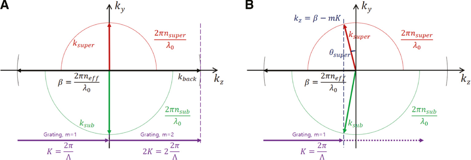
Although the analytic framework discussed here is based on a simple diffraction theory, it can predict various aspects of diffraction grating-based optical coupling behaviors with reasonable accuracy [116]. A grating coupler is usually composed of periodically located multiple diffractive elements, and the light diffraction angles from such optical structures can be described by the conventional diffraction theory and the so-called Bragg condition [84]. The Bragg condition for wavevectors parallel to the optical waveguide axis (z-axis in Figures 8 and 9, and in this section, we assume that the light propagation direction is toward –z from the integrated waveguide to the optical fiber) shows that the difference between the waveguide propagation constant (β=2π·neff/λ0, where neff is the effective refractive index of the waveguide and λ0 is the free-space optical wavelength) and the surface-parallel component of the wavevector of the diffracted wave (kz) should be matched to an integer multiple (m) of the grating’s wavevector (K=2π/Λ, where Λ is the grating period) and is given by β – kz=m·K. Depending on the input wavelength and grating period, multiple diffraction orders can be generated toward both the superstrate (diffracted toward the upward direction with a corresponding in-plane wavevector component of ksuper=2π ·nsuper/λ0) and the substrate (downward direction with an in-plane wavevector component of ksub=2π·nsub/λ0), as illustrated in Figure 9.
When the effective optical wavelength inside the waveguide (λ0/neff) matches the grating period (Λ=λ0/neff), the waveguide propagation constant (β) becomes equivalent to the grating’s wavevector (β=K), as shown in Figure 9A. In this case, the second-order diffraction (m=2) corresponds to the back-reflection (kback=β – 2K) toward the silicon waveguide [117] and inevitably reduces the optical power in the first-order diffracted beam (m=1) toward the vertical direction (kz=0). The vertically diffracted optical beam also has to go through multiple reflections between parallel optical interfaces, such as the silicon substrate, and therefore experiences Fabry-Pérot-type vertical oscillations. Therefore, such a grating coupler design with surface-normal diffraction (β=K, kx=0) is rarely used, and detuned off-normal grating designs are usually employed to improve the overall coupling efficiency [118], as shown in Figure 9B.
The diffraction angle to the superstrate (θsuper) is a crucial parameter for grating coupler designs, and the diffraction angle for the first order beam (m=1) can be expressed as neff – nsuper·sin θsuper=λ0/Λ. According to this relationship, the diffraction angle strongly depends on the grating period (Λ), the optical wavelength (λ0), and the effective index of the etched waveguide (neff). The effective refractive index for the waveguide also depends on the input polarization state. When the fill factor of the grating is f=W/Λ, where W is the width of the un-etched grating teeth, the effective index of the grating (neff) is approximately given by neff=f·neff, unetched+(1– f )·neff, etched, where neff, unetched and neff, etched represent the effective index of the unetched and etched grating slot, respectively [84]. The fundamental TM mode typically shows a smaller effective index than that of the fundamental TE mode [96]. As can be seen from this analysis, the main drawbacks of grating-based coupling are its strong wavelength and polarization dependence, which limits the operating wavelength range and input polarization states.
3.2 Apodized grating structures
A variety of apodized grating couplers with spatially varying fill factors and etch depths has been reported to achieve high coupling efficiencies with large overlap integral values between the field profiles of diffracted light from the grating coupler structure and the free-space propagating beam from the optical fiber, as schematically shown in Figure 10A. In this schematic illustration, unlike our previous convention used in the previous section (e.g. Figure 2), we assume that the light propagation direction is from the integrated waveguides (waveguide 2 in Figure 2) to the optical fibers (waveguide 1 in Figure 2) for simplicity. Due to the reciprocity theorem, this does not change the results. The uniform grating structures cannot achieve very high coupling efficiencies because the output beam diffracted through the grating structure has an exponentially decaying asymmetric electric field profile (E1′, top in Figure 10A), rather than having a Gaussian-like symmetric distribution (E1′, bottom in Figure 10A) similar to the fiber mode (∑E2,k) [119]. When the guided light in the waveguide is diffracted from an apodized grating coupler with spatially varying non-uniform grating elements, the output field distribution at the grating surface can resemble a Gaussian-like shape that can result in a higher mode overlap at the fiber facet [120], [121].
![Figure 10: Diffraction grating-based optical coupling with apodized grating.Schematic diagram of mode overlap difference between (A) the uniform and (B) apodized gratings. Depending on the grating apodization, exponentially decaying or Gaussian-like electric field profiles (red curves, E1′) are propagated from waveguide 1 (grating-based optical couplers) and Gaussian modes (blue curves, ∑E2,k) are the guided modes in waveguide 2 (optical fibers). (C, D) Cross-section and SEM image for the apodized grating couplers based on optimized fill factors. Adapted from Ref. [109]. Copyright (2013) The Optical Society.](/document/doi/10.1515/nanoph-2018-0075/asset/graphic/j_nanoph-2018-0075_fig_010.jpg)
Diffraction grating-based optical coupling with apodized grating.
Schematic diagram of mode overlap difference between (A) the uniform and (B) apodized gratings. Depending on the grating apodization, exponentially decaying or Gaussian-like electric field profiles (red curves, E1′) are propagated from waveguide 1 (grating-based optical couplers) and Gaussian modes (blue curves, ∑E2,k) are the guided modes in waveguide 2 (optical fibers). (C, D) Cross-section and SEM image for the apodized grating couplers based on optimized fill factors. Adapted from Ref. [109]. Copyright (2013) The Optical Society.
Figure 10B shows a shallow-etched apodized grating coupler with an optimized fill factor variation [122]. More specifically, the diffraction grating-based coupler was designed to provide an optical link between the single-mode optical fiber with a 10.4-μm MFD and the fundamental TE mode in the SOI-based PIC waveguide. The grating couplers were fabricated from an SOI wafer with a 340-nm-thick silicon device layer and a 2-μm-thick buried oxide layer. In order to achieve efficient mode matching and reduce back-reflection, the etch depth was optimized to 200 nm while the grating element fill factor was gradually changed from 0.08 to 0.4 along the waveguide propagation axis. As a result, the apodized grating structure achieved −1.2 dB (75.9%) efficiency at 1533 nm [122]. Recently, a high-efficiency grating coupler without a bottom reflector was reported by optimizing both the grating elements’ fill factor and their periodicity [111]. The theoretical coupling efficiency for such an optimized grating coupler was estimated to be −0.8 dB (83.2%), and the experimental coupling efficiency of −0.9 dB (81.3%) was obtained. The samples were fabricated on an SOI wafer with a 260-nm device layer by electron beam lithography and a single-etch fabrication process.
More recently, a coupling efficiency of −0.7 dB (85.1%) near the 1310-nm wavelength was obtained by dual-etch apodized grating couplers [123]. High-efficiency grating couplers can be realized with multi-step etching techniques [109], [110], [123] and SWG structures [100], [101], [124], [125]. For example, a grating coupler with multiple etch depths achieved −1.9 dB (64.6%) coupling efficiency (Figure 10C) [109]. Subwavelength-scale diffractive elements, such as a photonic crystal structure, can also be used to implement a more efficient grating coupler [125].
3.3 Directionality-enhanced grating structures
Directionality (Pup/Pwg) shows the fraction of the waveguide input power (Pwg) that is diffracted to the upward direction (Pup). One of the main factors that reduce the grating coupler’s coupling efficiency is its low directionality because a significant fraction (35%~45% [112]) of the input optical power to the waveguide is diffracted downward from the grating structure and becomes lost in the substrate, as shown in Figure 9. The basic rule of thumb for improving the directionality is to control the interference between the diffracted and reflected light components, which can be simply accomplished by tuning the thicknesses of the buried silicon oxide and cladding layers [114], [126] to maximize the outcoupled optical power toward the desired direction.
Figure 11A [127] schematically shows a method to improve the directionality with a substrate reflector, which is typically a Bragg reflector composed of alternating materials with high and low refractive indices, and reflects the downward diffracted light toward the upward direction to improve the directionality. Similar approaches have been introduced [113], [118], [127], [128], [129]. The reflectivity of the multilayer reflector is determined by the thicknesses of each layer, the refractive indices, and the number of such layers. For example, grating coupling structures with a Bragg bottom mirror made of Si/SiO2 layers were demonstrated, and the measured coupling efficiency was −1.58 dB (69.5%) with a 1-dB bandwidth of 36 nm [127], as shown in Figure 11B.
![Figure 11: Diffraction grating-based optical coupling methods using directionality-enhanced grating structures.(A) Schematic diagram of a grating coupler with a backside mirror, enhancing the upward power (Pup) using interference effects. (B) SEM image of an example of the substrate reflector structure. Reprinted from Ref. [127]. Copyright (2009) The Optical Society. (C) Schematic diagram of a grating coupler with an overlay grating structure to reduce leakage. (D) SEM image of an example of a silicon overlay structure. Reprinted from Ref. [112]. Copyright (2010) The Optical Society.](/document/doi/10.1515/nanoph-2018-0075/asset/graphic/j_nanoph-2018-0075_fig_011.jpg)
Diffraction grating-based optical coupling methods using directionality-enhanced grating structures.
(A) Schematic diagram of a grating coupler with a backside mirror, enhancing the upward power (Pup) using interference effects. (B) SEM image of an example of the substrate reflector structure. Reprinted from Ref. [127]. Copyright (2009) The Optical Society. (C) Schematic diagram of a grating coupler with an overlay grating structure to reduce leakage. (D) SEM image of an example of a silicon overlay structure. Reprinted from Ref. [112]. Copyright (2010) The Optical Society.
The directionality can also be enhanced by employing a single mirror-like layer. A metal layer, such as an aluminum or gold layer, is also usually used to realize such a mirror-like layer [114], [130], [131], [132], [133], and even an amorphous silicon layer can be adopted as a bottom mirror [134]. After the grating structures and the waveguides were defined on the SOI wafer, a SiO2 top cladding layer was deposited. Then, the substrate of the wafer underneath the grating area was etched, and finally, a bottom reflector layer was deposited. The maximum measured coupling efficiency was −2 dB (63.1%) with a 1-dB bandwidth of 29 nm. The bottom reflector layer can also be assembled to the grating structures using flip-chip bonding [114], [134].
In addition, overlay grating elements can also improve the directionality by achieving constructive interference of Pup and reducing light leakage to the silicon substrate, as schematically described in Figure 11C. An epitaxially grown silicon layer can be used as an additional degree of freedom to the grating coupler design [112], [115], [135], and an example of a SEM image of a typical overlay grating is shown in Figure 11D [112]. The additional silicon layer on the un-etched grating teeth introduces an additional degree of freedom in the grating coupler design, and both the directionality and coupling length of the grating could be simultaneously optimized, overcoming the typical trade-off between the directionality and coupling length [112], [135]. After the grating structures were defined, an additional silicon layer was deposited and subsequently patterned and etched. When the unnecessary silicon overlay was removed by dry etching, the maximum coupling efficiency and 1-dB bandwidth were measured to be −1.6 dB (69.2%) and 44 nm, respectively [112]. In ref. [115], two grating couplers were stacked by adding a second layer. Total film thickness was set to be 220 nm, and a simulated coupling efficiency of −0.137 dB was achieved.
Interleaved etching (dual-etch) processes were also adopted to improve directionality [136], [137]. A bi-level grating can be treated as a linear superposition of two gratings and generates constructive interference toward the superstrate and destructive interference toward the substrate [138]. Interleaved etching (70-nm and 220-nm depth) of a standard 220-nm-thick SOI platform resulted in a grating coupler with a coupling efficiency of −1.3 dB and a 3-dB bandwidth of 52 nm [137].
Enhancing the directionality is crucial to ensure that the grating coupler achieves high coupling efficiencies. The design strategies and fabrication schemes for the grating-based optical coupler should be carefully chosen considering the overall fabrication process flows and packaging situations.
4 Adiabatic coupling
Adiabatic coupling (or evanescent coupling) can achieve highly efficient wavelength-independent coupling between two adiabatically tapered waveguides. In this scheme, in order to match the effective modal index, both waveguides are inversely tapered to reduce the effective modal refractive index down to the refractive index of the surrounding cladding material(s) (e.g. silicon dioxide or air). Although the tapered waveguide geometries are also employed in the end-fire coupling schemes (Section 2.3 [39], [40], [41], [42], [56], [57], [58], [59], 62], [63], [64], [65], [66], [67] and Section 2.4 [43], [79]), the main difference in adiabatic coupling is that the optical power transfer between the input and output waveguides is achieved through evanescent coupling. In the end-fire coupling scheme, the optical power from the input waveguide arrives at the front facet of the output waveguide at which the coupling efficiency can be determined by the field overlap. However, for the adiabatic coupling scheme, the optical power transfer from the input waveguide to the output waveguide continuously occurs through evanescent coupling over the waveguide interaction region where two waveguides’ optical modes spatially overlap with each other. To facilitate evanescent power transfer, the waveguide dimensions need to be close to or within the subwavelength scale so that the optical mode profiles reside mostly outside the waveguide core region.
In the early 2000s, many research groups adopted tapered optical fibers for efficient optical power transmission to silica-based [139], [140], [141] and semiconductor-based microcavities [142]. For this type of waveguide-to-resonator coupling applications, critical coupling conditions between the access waveguide and the resonator are typically preferred for an optimal balance between the coupling loss and the resonator loss, and therefore, it does not require complete optical power transfer. Although the similarly tapered optical fibers are used for adiabatic coupling to and from the integrated PIC waveguides, the coupling regime is quite different from the critical coupling case.
Early works on adiabatic waveguide coupling were based on biconical tapered fibers [143], [144] and conical tapered fibers [145]. Emerging applications, such as single-photon-level integrated quantum optics, need very high optical coupling efficiency, close to 100%, which represent the extreme cases of reliable and predictable photon transfer between waveguides. In addition, the adiabatic waveguide coupling method can also be applied for testing and characterization of on-chip photonic components [146]. Table 3 lists the performances of various adiabatic coupling examples.
Summary of the reported adiabatic coupling methods.
| Ref. | Year | Fiber | Coupling (TE) efficiency (dB) | Operation wavelength (nm) | Fiber fabrication | Comments |
|---|---|---|---|---|---|---|
| [144] | 2004 | Biconical | −0.223 | 1565–1625 | Heating and pulling | Silicon WG/vertical coupling |
| [147] | 2013 | Biconical | −0.223 | 1550 | Heating and pulling | Silicon WG/vertical coupling |
| [145] | 2015 | Conical | −0.132 (−0.044*) | 780 | Heating and pulling | SIN WG/lateral coupling |
| [148] | 2016 | Biconical | −7.85~−4.32 (−1.549*) | 780 | Heating and pulling | Diamond WG/vertical coupling |
| [149] | 2017 | Conical | −0.362 | 780 | Chemical etching | Diamond WG/vertical coupling |
| [150] | 2018 | Conical | −0.017* | 1550 | Chemical etching | Silicon WG/lateral coupling |
The coupling efficiencies with “*” indicate the simulated results.
4.1 Principle of operation
To further improve the optical coupling efficiency of conventional end-fire coupling methods, the adiabatic waveguide coupling scheme uses a longer coupling distance with the slower transformation of the guided modes with the tapered input and output waveguides, as schematically shown in Figure 12A. The key idea of adiabatic light coupling between tapered fibers and inversely tapered waveguides is to slowly and adiabatically transform the waveguides modal cross-section along the propagation direction such that the propagating electromagnetic field profile remains in a single eigenmode through the composite waveguide region where both the tapered input and output waveguides overlap with each other (e.g. a combination of tapered optical fibers and silicon waveguides). To suppress higher order mode excitation and the corresponding optical losses, both waveguides should be gradually tapered and fulfill the adiabatic condition [151], [152]. For example, specially designed fibers, such as tapered and pulled fibers with wavelength- or subwavelength-scale core/cladding dimensions in contrast to the cleaved or lensed fibers in the previous sections, are used to efficiently generate evanescent optical fields. With adiabatically varying waveguides, the optical coupling length between two waveguides is given by λ0/(neff,1 – neff,2), where neff,1 and neff,2 are the effective refractive indices of the two eigenmodes [153]. As a result, nearly 100% power transfer can be obtained between two waveguides when the waveguide interaction length is longer than the coupling length, λ0/(neff,1 – neff,2).
![Figure 12: (A) Schematic diagram of the fiber-waveguide coupling scheme. (B) Adiabatic coupling between high-index SiN waveguide (right) and low-index tapered optical fiber (left). (C) The corresponding cross-sectional of |E|2 obtained from the FDTD simulations at various positions along the adiabatic couplers.Adapted from Ref. [145]. Copyright (2015) The Optical Society.](/document/doi/10.1515/nanoph-2018-0075/asset/graphic/j_nanoph-2018-0075_fig_012.jpg)
(A) Schematic diagram of the fiber-waveguide coupling scheme. (B) Adiabatic coupling between high-index SiN waveguide (right) and low-index tapered optical fiber (left). (C) The corresponding cross-sectional of |E|2 obtained from the FDTD simulations at various positions along the adiabatic couplers.
Adapted from Ref. [145]. Copyright (2015) The Optical Society.
4.2 Broadband optical coupling in the visible and infrared wavelength range
To obtain evanescent coupling between the optical fibers and the integrated waveguides, biconical tapered optical fibers were used [143], [144], [147], [148]. The waveguide interaction distance was up to ~25-μm long [147]. Single-sided conical tapered fibers can also be used for adiabatic coupling [145], [149], [150]. For single-sided conical tapered fiber fabrication, a chemical etching method was used [149], [150]. In contrast to the biconical fibers, single-sided geometries can offer better mechanical stability and compactness suitable for coupling with the PIC chips [145]. Highly efficient optical coupling, up to −0.13 dB (97%), was achieved with very compact coupling interfaces [145]. Figure 12B shows a schematic diagram of fiber-to-silicon nitride waveguide coupling [145]. By following the adiabatic tapering condition discussed in Section 4.1, the optical modes can be evanescently coupled between two waveguides, as shown in Figure 12C. The reported results have focused on the visible wavelength range operation with silicon nitride [145] and diamond [149] waveguides. High-efficiency optical coupling schemes with silicon waveguides in the near-infrared wavelengths were also proposed with an adiabatically tapered silica fiber whose full tip angle was ~1.2° [150].
The advantages of adiabatic coupling include a large 1-dB alignment tolerance dimensions up to ~50 μm along the waveguide optical axis [149], a wide 1-dB bandwidth larger than a wavelength range of 200 nm [147], [149], [150], and very high coupling efficiencies. However, in this scheme, the integrated waveguides need to be suspended and surrounded by lower index materials, such as air, to prevent the optical power leakage to the other cladding layers, and therefore, additional processing steps are required as in Section 2.3.
5 Conclusion
In this paper, we reviewed the development progress of three major light coupling methods between the optical fibers and the integrated waveguides for PICs: end-fire coupling, diffraction grating-based coupling, and adiabatic coupling. High-index material-based optical waveguide structures and their integration with other optical devices in the PIC platforms have resulted in large-scale integration and miniaturization of photonic devices and systems. For example, well-developed microfabrication technologies and infrastructures enable silicon-based integrated photonics to be a promising platform for large-scale heterogeneous optoelectronic integration and may provide economies of scaling and high manufacturing yields for integrated optoelectronics. However, high-efficiency transmission of optical signals into and out of such PIC platforms with a reliable yet cost-effective packaging solution is still an important and critical issue in solving the interface bottleneck.
The end-fire coupling methods, which were first introduced in the 1970s with relatively low port counts, require that the PIC chips be diced and cleaved. In order to provide wafer-level characterization capabilities and scalable interfaces between the optical fibers and PICs, surface-normal coupling methods using diffractive grating structures were introduced and resulted in greater layout design flexibilities and scalabilities in optical port counts. However, the grating-based methods typically show wavelength and polarization dependencies. More recently, adiabatic coupling methods have been introduced that can reduce the wavelength and polarization dependence while allowing more compact and wafer-scale interfaces to the optical fibers.
In addition to the three major coupling methods discussed in this paper, we expect that fiber-to-PIC coupling techniques will further evolve to meet the future needs to support various types of fibers and integrated optoelectronics platforms as well as advanced optical signaling formats. For example, multi-core or multimode fibers can take advantage of space division multiplexing technologies to provide compact multi-channel optical interfaces to the integrated photonic circuits. Emerging examples to provide a simple connectivity between multimode fibers and integrated photonic components, such as surface-normal emitters and detectors, include end-fire coupling [154] and grating-based coupling techniques [155]. One can envision that advances in photonics, especially nanophotonics, will enable highly efficient, reliable, and seamless optical interfaces between heterogeneous optical platforms for high-performance optoelectronic systems with higher coupling efficiencies and better alignment tolerances.
Acknowledgment
This work was supported by the research fund of Signal Intelligence Research Center supervised by Defense Acquisition Program Administration and Agency for Defense Development of Korea.
References
[1] Liu H, Lam CF, Johnson C. Scaling optical interconnects in datacenter networks opportunities and challenges for WDM. In: High Performance Interconnects (HOTI), 2010 IEEE 18th Annual Symposium on, IEEE, 2010:113–6.10.1109/HOTI.2010.15Search in Google Scholar
[2] Leuthold J, Koos C, Freude W. Nonlinear silicon photonics. Nat Photon 2010;4:535–44.10.1038/nphoton.2010.185Search in Google Scholar
[3] Van Laer R, Kuyken B, Van Thourhout D, Baets R. Interaction between light and highly confined hypersound in a silicon photonic nanowire. Nat Photon 2015;9:199–203.10.1038/nphoton.2015.11Search in Google Scholar
[4] Thompson JD, Tiecke T, de Leon NP, et al. Coupling a single trapped atom to a nanoscale optical cavity. Science 2013;340:1202–5.10.1126/science.1237125Search in Google Scholar PubMed
[5] Wagner R, Tomlinson W. Coupling efficiency of optics in single-mode fiber components. Appl Opt 1982;21:2671–88.10.1364/AO.21.002671Search in Google Scholar PubMed
[6] Keiser G. Optical fiber communications. 3rd ed. New York, McGraw-Hill, 2000.Search in Google Scholar
[7] Jalali B, Fathpour S. Silicon photonics. J Lightw Technol 2006;24:4600–15.10.1109/JLT.2006.885782Search in Google Scholar
[8] Dong P, Chen Y-K, Duan G-H, Neilson DT. Silicon photonic devices and integrated circuits. Nanophotonics 2014;3:215–28.10.1515/nanoph-2013-0023Search in Google Scholar
[9] Liang D, Roelkens G, Baets R, Bowers JE. Hybrid integrated platforms for silicon photonics. Materials 2010;3:1782–802.10.3390/ma3031782Search in Google Scholar
[10] Liang D, Bowers JE. Recent progress in lasers on silicon. Nat Photon 2010;4:511–7.10.1038/nphoton.2010.167Search in Google Scholar
[11] Vlasov YA, McNab SJ. Losses in single-mode silicon-on-insulator strip waveguides and bends. Opt Express 2004;12:1622–31.10.1364/OPEX.12.001622Search in Google Scholar PubMed
[12] Miller SE. Integrated optics: an introduction. Bell Labs Tech J 1969;48:2059–69.10.1002/j.1538-7305.1969.tb01165.xSearch in Google Scholar
[13] Henry CH, Blonder G, Kazarinov R. Glass waveguides on silicon for hybrid optical packaging. J Lightw Technol 1989;7:1530–9.10.1109/50.39094Search in Google Scholar
[14] Kawachi M. Silica waveguides on silicon and their application to integrated-optic components. Opt Quant Electron 1990;22:391–416.10.1007/BF02113964Search in Google Scholar
[15] Van Laere F, Roelkens G, Ayre M, et al. Compact and highly efficient grating couplers between optical fiber and nanophotonic waveguides. J Lightw Technol 2007;25:151–6.10.1109/JLT.2006.888164Search in Google Scholar
[16] Boivin L. Thin-film laser-to-fiber coupler. Appl Opt 1974;13: 391–5.10.1364/AO.13.000391Search in Google Scholar PubMed
[17] Hunsperger RG, Yariv A, Lee A. Parallel end-butt coupling for optical integrated circuits. Appl Opt 1977;16:1026–32.10.1364/AO.16.001026Search in Google Scholar PubMed
[18] Kuwahara H, Sasaki M, Tokoyo N. Efficient coupling from semiconductor lasers into single-mode fibers with tapered hemispherical ends. Appl Opt 1980;19:2578–83.10.1364/AO.19.002578Search in Google Scholar PubMed
[19] Bulmer C, Sheem S, Moeller R, Burns W. High-efficiency flip-chip coupling between single-mode fibers and LiNbO3 channel waveguides. Appl Phys Lett 1980;37:351–3.10.1063/1.91944Search in Google Scholar
[20] Hsu H, Milton A. Flip-chip approach to endfire coupling between single-mode optical fibres and channel waveguides. Electron Lett 1976;12:404–5.10.1049/el:19760309Search in Google Scholar
[21] Schmidt R, Buhl L. Experimental 4×4 optical switching network. Electron Lett 1976;12:575–7.10.1049/el:19760439Search in Google Scholar
[22] Burns WK, Hocker G. End fire coupling between optical fibers and diffused channel waveguides. Appl Opt 1977;16:2048–50.10.1364/AO.16.002048Search in Google Scholar PubMed
[23] Noda J, Mikami O, Minakata M, Fukuma M. Single-mode optical-waveguide fiber coupler. Appl Opt 1978;17:2092–6.10.1364/AO.17.002092Search in Google Scholar PubMed
[24] Keil R, Auracher F. Coupling of single-mode Ti-diffused LiNbO3 waveguides to single-mode fibers. Opt Commun 1979;30:23–8.10.1016/0030-4018(79)90034-8Search in Google Scholar
[25] Kasaya K, Mitomi O, Naganuma M, Kondo Y, Noguchi Y. A simple laterally tapered waveguide for low-loss coupling to single-mode fibers. IEEE Photon Technol Lett 1993;5:345–7.10.1109/68.205633Search in Google Scholar
[26] Alder T, Stohr A, Heinzelmann R, Jager D. High-efficiency fiber-to-chip coupling using low-loss tapered single-mode fiber. IEEE Photon Technol Lett 2000;12:1016–8.10.1109/68.867993Search in Google Scholar
[27] Lealman I, Rivers L, Harlow M, Perrin S. InGaAsP/InP tapered active layer multiquantum well laser with 1.8 dB coupling loss to cleaved singlemode fibre. Electron Lett 1994;30:1685–7.10.1049/el:19941156Search in Google Scholar
[28] Thurston RN, Kapon E, Shahar A. Two-dimensional control of mode size in optical channel waveguides by lateral channel tapering. Opt Lett 1991;16:306–8.10.1364/OL.16.000306Search in Google Scholar PubMed
[29] Taillaert D, Bogaerts W, Bienstman P, et al. An out-of-plane grating coupler for efficient butt-coupling between compact planar waveguides and single-mode fibers. IEEE J Quant Electron 2002;38:949–55.10.1109/JQE.2002.1017613Search in Google Scholar
[30] Vusirikala V, Gopalan B, Kareenahalli S, et al. GaAs-AlGaAs QW diluted waveguide laser with low-loss, alignment-tolerant coupling to a single-mode fiber. IEEE Photon Technol Lett 1996;8:1130–2.10.1109/68.531812Search in Google Scholar
[31] Latry O, Ketata M, Ketata K, Debrie R. Optimization of the coupling between a tapered fibre and a pin photodiode. J Phys D 1995;28:1562.10.1088/0022-3727/28/8/004Search in Google Scholar
[32] Karioja P, Howe D. Diode-laser-to-waveguide butt coupling. Appl Opt 1996;35:404–16.10.1364/AO.35.000404Search in Google Scholar PubMed
[33] Sure A, Dillon T, Murakowski J, Lin C, Pustai D, Prather DW. Fabrication and characterization of three-dimensional silicon tapers. Opt Express 2003;11:3555–61.10.1364/OE.11.003555Search in Google Scholar PubMed
[34] Fritze M, Knecht J, Bozler C, et al. Fabrication of three-dimensional mode converters for silicon-based integrated optics. J Vac Sci Technol B 2003;21:2897–902.10.1116/1.1625967Search in Google Scholar
[35] Shiraishi K, Yoda H, Ohshima A, Ikedo H, Tsai CS. A silicon-based spot-size converter between single-mode fibers and Si-wire waveguides using cascaded tapers. Appl Phys Lett 2007;91:141120-1–3.10.1063/1.2795337Search in Google Scholar
[36] Yang Z, Fang N, Wu A, et al. Fabrication and characterization of integrated three-dimensional linear taper on silicon-on-insulator. Opt Eng 2009;48:030503-1–3.10.1117/1.3095916Search in Google Scholar
[37] Fang N, Yang Z, Wu A, et al. Three-dimensional tapered spot-size converter based on (111) silicon-on-insulator. IEEE Photon Technol Lett 2009;21:820–2.10.1109/LPT.2009.2019619Search in Google Scholar
[38] Shoji T, Tsuchizawa T, Watanabe T, Yamada K, Morita H. Low loss mode size converter from 0.3 μm square Si wire waveguides to singlemode fibres. Electron Lett 2002;38:1669–70.10.1049/el:20021185Search in Google Scholar
[39] Pu M, Liu L, Ou H, Yvind K, Hvam JM. Ultra-low-loss inverted taper coupler for silicon-on-insulator ridge waveguide. Opt Commun 2010;283:3678–82.10.1016/j.optcom.2010.05.034Search in Google Scholar
[40] Park H, Kim S, Park J, Joo J, Kim G. A fiber-to-chip coupler based on Si/SiON cascaded tapers for Si photonic chips. Opt Express 2013;21:29313–9.10.1364/OE.21.029313Search in Google Scholar PubMed
[41] Chen L, Doerr CR, Chen Y-K, Liow T-Y. Low-loss and broadband cantilever couplers between standard cleaved fibers and high-index-contrast Si3N4 or Si waveguides. IEEE Photon Technol Lett 2010;22:1744–6.10.1109/LPT.2010.2085040Search in Google Scholar
[42] Jia L, Li C, Liow T-Y, Lo G-Q. Efficient suspended coupler with loss less than −1.4 dB between Si-photonic waveguide and cleaved single mode fiber. J Lightw Technol 2018;36:239–44.10.1109/JLT.2017.2779863Search in Google Scholar
[43] Wood M, Sun P, Reano RM. Compact cantilever couplers for low-loss fiber coupling to silicon photonic integrated circuits. Opt Express 2012;20:164–72.10.1364/OE.20.000164Search in Google Scholar PubMed
[44] Yoshida T, Omoda E, Atsumi Y, et al. Vertically curved Si waveguide coupler with low loss and flat wavelength window. J Lightw Technol 2016;34:1567–71.10.1109/JLT.2015.2506732Search in Google Scholar
[45] Solgaard O. Photonic microsystems: micro and nanotechnology applied to optical devices and systems. New York, Springer, 2009.10.1007/978-0-387-68351-5_15Search in Google Scholar
[46] Kasaya K, Kondo Y, Okamoto M, Mitomi O, Naganuma M. Monolithically integrated DBR lasers with simple tapered waveguide for low-loss fibre coupling. Electron Lett 1993;29:2067–8.10.1049/el:19931381Search in Google Scholar
[47] Walpole J, Liau Z, Missaggia L, Yap D. Diode lasers with cylindrical mirror facets and reduced beam divergence. Appl Phys Lett 1987;50:1219–21.10.1063/1.97914Search in Google Scholar
[48] Moerman I, D’Hondt M, Vanderbauwhede W, Van Daele P, Demeester P, Hunziker W. InGaAsP/lnP strained MQW laser with integrated mode size converter using the shadow masked growth technique. Electron Lett 1995;31:452–4.10.1049/el:19950340Search in Google Scholar
[49] Brenner T, Melchior H. Integrated optical modeshape adapters in InGaAsP/InP for efficient fiber-to-waveguide coupling. IEEE Photon Technol Lett 1993;5:1053–6.10.1109/68.257189Search in Google Scholar
[50] Yoshimoto N, Kawano K, Takeuchi H, Kondo S, Noguchi Y. Spot size convertors using InP/InAlAs multiquantum well waveguides for low-loss singlemode fibre coupling. Electron Lett 1992;28;1610–1.10.1049/el:19921024Search in Google Scholar
[51] Moerman I, Van Daele PP, Demeester PM. A review on fabrication technologies for the monolithic integration of tapers with III-V semiconductor devices. IEEE J Selected Topics Quantum Electron 1998;3:1308–20.10.1109/2944.658785Search in Google Scholar
[52] Fijol JJ, Fike EE, Keating PB, et al. Fabrication of silicon-on-insulator adiabatic tapers for low-loss optical interconnection of photonic devices. In: Photonics packaging and integration III, International Society for Optics and Photonics, 2003;4997:157–71.10.1117/12.479371Search in Google Scholar
[53] Takei R, Suzuki M, Omoda E, et al. Silicon knife-edge taper waveguide for ultralow-loss spot-size converter fabricated by photolithography. Appl Phys Lett 2013;102:101108-1–4.10.1063/1.4795308Search in Google Scholar
[54] Yamaguchi N, Kokubun Y, Sato K. Low-loss spot-size transformer by dual tapered waveguides (DTW-SST). J Lightw Technol 1990;8:587–94.10.1109/50.50765Search in Google Scholar
[55] Almeida VR, Panepucci RR, Lipson M. Nanotaper for compact mode conversion. Opt Lett 2003;28:1302–4.10.1364/OL.28.001302Search in Google Scholar PubMed
[56] McNab SJ, Moll N, Vlasov YA. Ultra-low loss photonic integrated circuit with membrane-type photonic crystal waveguides. Opt Express 2003;11:2927–39.10.1364/OE.11.002927Search in Google Scholar PubMed
[57] Roelkens G, Van Thourhout D, Baets R, Nötzel R, Smit M. Laser emission and photodetection in an InP/InGaAsP layer integrated on and coupled to a silicon-on-insulator waveguide circuit. Opt Express 2006;14:8154–9.10.1364/OE.14.008154Search in Google Scholar PubMed
[58] Dangel R, Hofrichter J, Horst F, et al. Polymer waveguides for electro-optical integration in data centers and high-performance computers. Opt Express 2015;23:4736–50.10.1364/OE.23.004736Search in Google Scholar PubMed
[59] Shani Y, Henry C, Kistler R, Orlowsky K, Ackerman D. Efficient coupling of a semiconductor laser to an optical fiber by means of a tapered waveguide on silicon. Appl Phys Lett 1989;55:2389–91.10.1063/1.102290Search in Google Scholar
[60] Shu J, Qiu C, Zhang X, Xu Q. Efficient coupler between chip-level and board-level optical waveguides. Opt Lett 2011;36:3614–6.10.1364/OL.36.003614Search in Google Scholar PubMed
[61] Cardenas J, Poitras CB, Luke K, Luo L-W, Morton PA, Lipson M. High coupling efficiency etched facet tapers in silicon waveguides. IEEE Photon Technol Lett 2014;26:2380–2.10.1109/LPT.2014.2357177Search in Google Scholar
[62] Papes M, Cheben P, Benedikovic D, et al. Fiber-chip edge coupler with large mode size for silicon photonic wire waveguides. Opt Express 2016;24:5026–38.10.1364/OE.24.005026Search in Google Scholar PubMed
[63] Fang Q, Song J, Tao S, Yu M, Lo G, Kwong D. Low loss (~6.45 dB/cm) sub-micron polycrystalline silicon waveguide integrated with efficient SiON waveguide coupler. Opt Express 2008;16:6425–32.10.1364/OE.16.006425Search in Google Scholar PubMed
[64] Fang Q, Liow T-Y, Song JF, et al. Suspended optical fiber-to-waveguide mode size converter for silicon photonics. Opt Express 2010;18:7763–9.10.1364/OE.18.007763Search in Google Scholar PubMed
[65] Fang Q, Song J, Luo X, Yu M, Lo G, Liu Y. Mode-size converter with high coupling efficiency and broad bandwidth. Opt Express 2011;19:21588–94.10.1364/OE.19.021588Search in Google Scholar PubMed
[66] Fang Q, Song J, Luo X, et al. Low loss fiber-to-waveguide converter with a 3-D functional taper for silicon photonics. IEEE Photon Technol Lett 2016;28:2533–6.10.1109/LPT.2016.2602366Search in Google Scholar
[67] Jia L, Song J, Liow T-Y, et al. Mode size converter between high-index-contrast waveguide and cleaved single mode fiber using SiON as intermediate material. Opt Express 2014;22:23652–60.10.1364/OE.22.023652Search in Google Scholar PubMed
[68] Barwicz T, Lichoulas TW, Taira Y, et al. Automated, high-throughput photonic packaging. Opt Fiber Technol 2018;44:24–35.10.1016/j.yofte.2018.02.019Search in Google Scholar
[69] Barwicz T, Taira Y. Low-cost interfacing of fibers to nanophotonic waveguides: design for fabrication and assembly tolerances. IEEE Photon J 2014;6:1–18.10.1109/JPHOT.2014.2331251Search in Google Scholar
[70] Doany FE, Lee BG, Assefa S, et al. Multichannel high-bandwidth coupling of ultradense silicon photonic waveguide array to standard-pitch fiber array. J Lightw Technol 2011;29:475–82.10.1109/JLT.2010.2088110Search in Google Scholar
[71] Lindenmann N, Dottermusch S, Goedecke ML, et al. Connecting silicon photonic circuits to multicore fibers by photonic wire bonding. J Lightw Technol 2015;33:755–60.10.1109/JLT.2014.2373051Search in Google Scholar
[72] Lindenmann N, Balthasar G, Hillerkuss D, et al. Photonic wire bonding: a novel concept for chip-scale interconnects. Opt Express 2012;20:17667–77.10.1364/OE.20.017667Search in Google Scholar PubMed
[73] Billah MR, Blaicher M, Hoose T, et al. Hybrid integration of silicon photonics circuits and InP lasers by photonic wire bonding. Optica 2018;5:876–83.10.1364/OPTICA.5.000876Search in Google Scholar
[74] Dietrich PI, Blaicher M, Reuter I, et al. In situ 3D nanoprinting of free-form coupling elements for hybrid photonic integration. Nat Photon 2018;12:241–7.10.1038/s41566-018-0133-4Search in Google Scholar
[75] Tian Z-N, Wang L-J, Chen Q-D, et al. Beam shaping of edge-emitting diode lasers using a single double-axial hyperboloidal micro-lens. Opt Lett 2013;38:5414–7.10.1364/OL.38.005414Search in Google Scholar PubMed
[76] Cheben P, Bock PJ, Schmid JH, et al. Refractive index engineering with subwavelength gratings for efficient microphotonic couplers and planar waveguide multiplexers. Opt Lett 2010;35:2526–8.10.1364/OL.35.002526Search in Google Scholar PubMed
[77] Barwicz T, Janta-Polczynski A, Khater M, et al. An O-band metamaterial converter interfacing standard optical fibers to silicon nanophotonic waveguides. In: Optical Fiber Communication Conference, Optical Society of America, 2015, Th3F. 3.10.1364/OFC.2015.Th3F.3Search in Google Scholar
[78] Cheben P, Schmid JH, Wang S, et al. Broadband polarization independent nanophotonic coupler for silicon waveguides with ultra-high efficiency. Opt Express 2015;23:22553–63.10.1364/OE.23.022553Search in Google Scholar PubMed
[79] Sun P, Reano RM. Cantilever couplers for intra-chip coupling to silicon photonic integrated circuits. Opt Express 2009;17:4565–74.10.1364/OE.17.004565Search in Google Scholar PubMed
[80] Yoshida T, Tajima S, Takei R, Mori M, Miura N, Sakakibara Y. Vertical silicon waveguide coupler bent by ion implantation. Opt Express 2015;23:29449–56.10.1364/OE.23.029449Search in Google Scholar PubMed
[81] Ollier E. Optical MEMS devices based on moving waveguides. IEEE J Selected Topics Quantum Electron 2002;8:155–62.10.1109/2944.991411Search in Google Scholar
[82] Yoshida T, Nagao M, Kanemaru S. Development of thin-film bending technique induced by ion-beam irradiation. Appl Phys Express 2009;2:066501-1–3.10.1143/APEX.2.066501Search in Google Scholar
[83] Sun P, Reano RM. Vertical chip-to-chip coupling between silicon photonic integrated circuits using cantilever couplers. Opt Express 2011;19:4722–7.10.1364/OE.19.004722Search in Google Scholar PubMed
[84] Chrostowski L, Hochberg M. Silicon photonics design: from devices to systems. Cambridge, Cambridge University Press, 2015.10.1017/CBO9781316084168Search in Google Scholar
[85] Bozzola A, Carroll L, Gerace D, Cristiani I, Andreani LC. Optimising apodized grating couplers in a pure SOI platform to −0.5 dB coupling efficiency. Opt Express 2015;23:16289–304.10.1364/OE.23.016289Search in Google Scholar PubMed
[86] Aoyagi T, Aoyagi Y, Namba S. High-efficiency blazed grating couplers. Appl Phys Lett 1976;29:303–4.10.1063/1.89055Search in Google Scholar
[87] Dakss M, Kuhn L, Heidrich P, Scott B. Grating coupler for efficient excitation of optical guided waves in thin films. Appl Phys Lett 1970;16:523–5.10.1063/1.1653091Search in Google Scholar
[88] Kogelnik H, Sosnowski T. Holographic thin film couplers. Bell Labs Tech J 1970;49:1602–8.10.1002/j.1538-7305.1970.tb01846.xSearch in Google Scholar
[89] Burnham R, Scifres D, Streifer W. Low-divergence beams from grating-coupled composite guide heterostructure GaAlAs diode lasers. Appl Phys Lett 1975;26:644–7.10.1063/1.88011Search in Google Scholar
[90] Macomber S, Mott J, Noll R, et al. Surface-emitting distributed feedback semiconductor laser. Appl Phys Lett 1987;51:472–4.10.1063/1.98397Search in Google Scholar
[91] Streifer W, Scifres D, Burnham R. Analysis of grating-coupled radiation in GaAs: GaAlAs lasers and waveguides-I. IEEE J Quant Electron 1976;12:422–8.10.1109/JQE.1976.1069175Search in Google Scholar
[92] Peng S, Tamir T. Directional blazing of waves guided by asymmetrical dielectric gratings. Opt Commun 1974;11:405–9.10.1016/0030-4018(74)90247-8Search in Google Scholar
[93] Ang T, Reed G, Vonsovici A, Evans A, Routley P, Josey M. Effects of grating heights on highly efficient unibond SOI waveguide grating couplers. IEEE Photon Technol Lett 2000;12:59–61.10.1109/68.817493Search in Google Scholar
[94] El Melhaoui L. Light injection in SOI microwaveguides using high-efficiency grating couplers. J Lightw Technol 2006;24:3810–5.10.1109/JLT.2006.878060Search in Google Scholar
[95] Van Laere F, Claes T, Schrauwen J, et al. Compact focusing grating couplers for silicon-on-insulator integrated circuits. IEEE Photon Technol Lett 2007;19:1919–21.10.1109/LPT.2007.908762Search in Google Scholar
[96] Tailaert D, Chong H, Borel PI, Frandsen LH, De La Rue RM, Baets R. A compact two-dimensional grating coupler used as a polarization splitter. IEEE Photon Technol Lett 2003;15:1249–51.10.1109/LPT.2003.816671Search in Google Scholar
[97] Tang Y, Dai D, He S. Proposal for a grating waveguide serving as both a polarization splitter and an efficient coupler for silicon-on-insulator nanophotonic circuits. IEEE Photon Technol Lett 2009;21:242–4.10.1109/LPT.2008.2010528Search in Google Scholar
[98] Lacava C, Carrol L, Bozzola A, et al. Design and characterization of low-loss 2D grating couplers for silicon photonics integrated circuits. In: Silicon photonics XI, International Society for Optics and Photonics, 2016;9752:97520V.10.1117/12.2212458Search in Google Scholar
[99] Carroll L, Gerace D, Cristiani I, Andreani LC. Optimizing polarization-diversity couplers for Si-photonics: reaching the − 1dB coupling efficiency threshold. Opt Express 2014;22:14769–81.10.1364/OE.22.014769Search in Google Scholar PubMed
[100] Halir R, Cheben P, Schmid J, et al. Continuously apodized fiber-to-chip surface grating coupler with refractive index engineered subwavelength structure. Opt Lett 2010;35:3243–5.10.1364/OL.35.003243Search in Google Scholar PubMed
[101] Benedikovic D, Cheben P, Schmid JH, et al. High-efficiency single etch step apodized surface grating coupler using subwavelength structure. Laser Photon Rev 2014;8:L93–7.10.1002/lpor.201400113Search in Google Scholar
[102] Benedikovic D, Cheben P, Schmid JH, et al. Subwavelength index engineered surface grating coupler with sub-decibel efficiency for 220-nm silicon-on-insulator waveguides. Opt Express 2015;23:22628–35.10.1364/OE.23.022628Search in Google Scholar PubMed
[103] Chen X, Tsang HK. Polarization-independent grating couplers for silicon-on-insulator nanophotonic waveguides. Opt Lett 2011;36:796–8.10.1364/OL.36.000796Search in Google Scholar PubMed
[104] Xu X, Subbaraman H, Covey J, Kwong D, Hosseini A, Chen RT. Colorless grating couplers realized by interleaving dispersion engineered subwavelength structures. Opt Lett 2013;38:3588–91.10.1364/OL.38.003588Search in Google Scholar PubMed
[105] Hwang HY, Lee JS, Seok TJ, et al. Flip chip packaging of digital silicon photonics MEMS switch for cloud computing and data centre. IEEE Photon J 2017;9:1–10.10.1109/JPHOT.2017.2704097Search in Google Scholar
[106] Scarcella C, Gradkowski K, Carroll L, et al. Pluggable single-mode fiber-array-to-PIC coupling using micro-lenses. IEEE Photon Technol Lett 2017;29:1943–6.10.1109/LPT.2017.2757082Search in Google Scholar
[107] Seok TJ, Kopp VI, Neugroschl D, Henriksson J, Luo J, Wu MC. High density optical packaging of high radix silicon photonic switches. In: Optical Fiber Communication Conference, Optical Society of America, 2017, Th5D. 7.10.1364/OFC.2017.Th5D.7Search in Google Scholar
[108] Ding Y, Ye F, Peucheret C, Ou H, Miyamoto Y, Morioka T. On-chip grating coupler array on the SOI platform for fan-in/fan-out of MCFs with low insertion loss and crosstalk. Opt Express 2015;23:3292–8.10.1364/OE.23.003292Search in Google Scholar PubMed
[109] Tang Y, Wang Z, Wosinski L, Westergren U, He S. Highly efficient nonuniform grating coupler for silicon-on-insulator nanophotonic circuits. Opt Lett 2010;35:1290–2.10.1364/OL.35.001290Search in Google Scholar PubMed
[110] Li C, Zhang H, Yu M, Lo G. CMOS-compatible high efficiency double-etched apodized waveguide grating coupler. Opt Express 2013;21:7868–74.10.1364/OE.21.007868Search in Google Scholar PubMed
[111] Marchetti R, Lacava C, Khokhar A, et al. High-efficiency grating-couplers: demonstration of a new design strategy. Sci Rep 2017;7:16670-1–8.10.1038/s41598-017-16505-zSearch in Google Scholar PubMed PubMed Central
[112] Vermeulen D, Selvaraja S, Verheyen P, et al. High-efficiency fiber-to-chip grating couplers realized using an advanced CMOS-compatible silicon-on-insulator platform. Opt Express 2010;18:18278–83.10.1364/OE.18.018278Search in Google Scholar PubMed
[113] Mekis A, Abdalla S, Foltz D, et al. A CMOS photonics platform for high-speed optical interconnects. In: Photonics Conference (IPC), 2012 IEEE, IEEE, 2012:356–7.10.1109/IPCon.2012.6358639Search in Google Scholar
[114] Ding Y, Peucheret C, Ou H, Yvind K. Fully etched apodized grating coupler on the SOI platform with −0.58 dB coupling efficiency. Opt Lett 2014;39:5348–50.10.1364/OL.39.005348Search in Google Scholar PubMed
[115] Michaels A, Yablonovitch E. Inverse design of near unity efficiency perfectly vertical grating couplers. Opt Express 2018;26:4766–79.10.1364/OE.26.004766Search in Google Scholar PubMed
[116] Wang Y, Flueckiger J, Lin C, Chrostowski L. Universal grating coupler design. In: Photonics North 2013, International Society for Optics and Photonics, 2013;8915:89150Y.10.1117/12.2042185Search in Google Scholar
[117] Roelkens G, Vermeulen D, Selvaraja S, Halir R, Bogaerts W, Van Thourhout D. Grating-based optical fiber interfaces for silicon-on-insulator photonic integrated circuits. IEEE J Selected Topics Quantum Electron 2011;17:571–80.10.1109/JSTQE.2010.2069087Search in Google Scholar
[118] Taillaert D, Bienstman P, Baets R. Compact efficient broadband grating coupler for silicon-on-insulator waveguides. Opt Lett 2004;29:2749–51.10.1364/OL.29.002749Search in Google Scholar PubMed
[119] Taillaert D, Van Laere F, Ayre M, et al. Grating couplers for coupling between optical fibers and nanophotonic waveguides. Jpn J Appl Phys 2006;45:6071–7.10.1143/JJAP.45.6071Search in Google Scholar
[120] Waldhäusl R, Schnabel B, Dannberg P, Kley E-B, Bräuer A, Karthe W. Efficient coupling into polymer waveguides by gratings. Appl Opt 1997;36:9383–90.10.1364/AO.36.009383Search in Google Scholar PubMed
[121] Bates KA, Li L, Roncone RL, Burke JJ. Gaussian beams from variable groove depth grating couplers in planar waveguides. Appl Opt 1993;32:2112–6.10.1364/AO.32.002112Search in Google Scholar PubMed
[122] Chen X, Li C, Fung CK, Lo SM, Tsang HK. Apodized waveguide grating couplers for efficient coupling to optical fibers. IEEE Photon Technol Lett 2010;22:1156–8.10.1109/LPT.2010.2051220Search in Google Scholar
[123] Chen X, Thomson DJ, Crudginton L, Khokhar AZ, Reed GT. Dual-etch apodised grating couplers for efficient fibre-chip coupling near 1310 nm wavelength. Opt Express 2017;25:17864–71.10.1364/OE.25.017864Search in Google Scholar PubMed
[124] Xu X, Subbaraman H, Covey J, Kwong D, Hosseini A, Chen RT. Complementary metal–oxide–semiconductor compatible high efficiency subwavelength grating couplers for silicon integrated photonics. Appl Phys Lett 2012;101:031109-1–4.10.1063/1.4737412Search in Google Scholar
[125] Ding Y, Ou H, Peucheret C. Ultrahigh-efficiency apodized grating coupler using fully etched photonic crystals. Opt Lett 2013;38:2732–4.10.1364/OL.38.002732Search in Google Scholar PubMed
[126] Emmons RM, Hall DG. Buried-oxide silicon-on-insulator structures. II. Waveguide grating couplers. IEEE J Quant Electron 1992;28:164–75.10.1109/3.119511Search in Google Scholar
[127] Selvaraja SK, Vermeulen D, Schaekers M, et al. Highly efficient grating coupler between optical fiber and silicon photonic circuit. In: Conference on Lasers and Electro-Optics, Optical Society of America, 2009, CTuC6.10.1364/CLEO.2009.CTuC6Search in Google Scholar
[128] Hardy A, Welch DF, Streifer W. Analysis of second-order gratings. IEEE J Quant Electron 1989;25:2096–105.10.1109/3.35721Search in Google Scholar
[129] Suhara T, Nishihara H. Integrated optics components and devices using periodic structures. IEEE J Quant Electron 1986;22:845–67.10.1109/JQE.1986.1073051Search in Google Scholar
[130] Orobtchouk R, Layadi A, Gualous H, Pascal D, Koster A, Laval S. High-efficiency light coupling in a submicrometric silicon-on-insulator waveguide. Appl Opt 2000;39:5773–7.10.1364/AO.39.005773Search in Google Scholar
[131] Zaoui WS, Kunze A, Vogel W, Berroth M. CMOS-compatible polarization splitting grating couplers with a backside metal mirror. IEEE Photon Technol Lett 2013;25:1395–7.10.1109/LPT.2013.2266132Search in Google Scholar
[132] Zaoui WS, Kunze A, Vogel W, et al. Bridging the gap between optical fibers and silicon photonic integrated circuits. Opt Express 2014;22:1277–86.10.1364/OE.22.001277Search in Google Scholar PubMed
[133] Zaoui WS, Rosa MF, Vogel W, Berroth M, Butschke J, Letzkus F. Cost-effective CMOS-compatible grating couplers with backside metal mirror and 69% coupling efficiency. Opt Express 2012;20:B238–43.10.1364/OE.20.00B238Search in Google Scholar PubMed
[134] Kopp C, Augendre E, Orobtchouk R, Lemonnier O, Fedeli J-M. Enhanced fiber grating coupler integrated by wafer-to-wafer bonding. J Lightw Technol 2011;29:1847–51.10.1109/JLT.2011.2146755Search in Google Scholar
[135] Roelkens G, Van Thourhout D, Baets R. High efficiency silicon-on-insulator grating coupler based on a poly-Silicon overlay. Opt Express 2006;14:11622–30.10.1364/OE.14.011622Search in Google Scholar PubMed
[136] Fan M, Popovic MA, Kartner FX. High directivity, vertical fiber-to-chip coupler with anisotropically radiating grating teeth. In: Lasers and electro-optics, 2007. CLEO 2007. Conference on, IEEE, 2007:1–2.10.1109/CLEO.2007.4452953Search in Google Scholar
[137] Benedikovic D, Alonso-Ramos C, Cheben P, et al. High-directionality fiber-chip grating coupler with interleaved trenches and subwavelength index-matching structure. Opt Lett 2015;40:4190–3.10.1364/OL.40.004190Search in Google Scholar PubMed
[138] Flory CA. Analysis of directional grating-coupled radiation in waveguide structures. IEEE J Quant Electron 2004;40:949–57.10.1109/JQE.2004.830179Search in Google Scholar
[139] Collot L, Lefevre-Seguin V, Brune M, Raimond J, Haroche S. Very high-Q whispering-gallery mode resonances observed on fused silica microspheres. EPL (Europhysics Letters) 1993;23:327–34.10.1209/0295-5075/23/5/005Search in Google Scholar
[140] Spillane S, Kippenberg T, Vahala K. Ultralow-threshold Raman laser using a spherical dielectric microcavity. Nature 2002;415:621–3.10.1038/415621aSearch in Google Scholar PubMed
[141] Armani D, Kippenberg T, Spillane S, Vahala K. Ultra-high-Q toroid microcavity on a chip. Nature 2003;421:925–8.10.1038/nature01371Search in Google Scholar PubMed
[142] Srinivasan K, Painter O. Linear and nonlinear optical spectroscopy of a strongly coupled microdisk–quantum dot system. Nature 2007;450:862–5.10.1038/nature06274Search in Google Scholar PubMed
[143] Barclay PE, Srinivasan K, Borselli M, Painter O. Efficient input and output fiber coupling to a photonic crystal waveguide. Opt Lett 2004;29:697–9.10.1364/OL.29.000697Search in Google Scholar PubMed
[144] Barclay PE, Srinivasan K, Borselli M, Painter O. Probing the dispersive and spatial properties of photonic crystal waveguides via highly efficient coupling from fiber tapers. Appl Phys Lett 2004;85:4–6.10.1063/1.1767954Search in Google Scholar
[145] Tiecke T, Nayak K, Thompson J, et al. Efficient fiber-optical interface for nanophotonic devices. Optica 2015;2:70–5.10.1364/OPTICA.2.000070Search in Google Scholar
[146] Michael C, Borselli M, Johnson T, Chrystal C, Painter O. An optical fiber-taper probe for wafer-scale microphotonic device characterization. Opt Express 2007;15:4745–52.10.1364/OE.15.004745Search in Google Scholar PubMed
[147] Gröblacher S, Hill JT, Safavi-Naeini AH, Chan J, Painter O. Highly efficient coupling from an optical fiber to a nanoscale silicon optomechanical cavity. Appl Phys Lett 2013;103:181104.10.1063/1.4826924Search in Google Scholar
[148] Patel RN, Schröder T, Wan N, et al. Efficient photon coupling from a diamond nitrogen vacancy center by integration with silica fiber. Light Sci Appl 2016;5:e16032-1–6.10.1038/lsa.2016.32Search in Google Scholar PubMed PubMed Central
[149] Burek MJ, Meuwly C, Evans RE, et al. Fiber-coupled diamond quantum nanophotonic interface. Phys Rev Appl 2017;8:024026-1–10.10.1103/PhysRevApplied.8.024026Search in Google Scholar
[150] Son G, Yu K. High-efficiency power transfer for silicon-based photonic devices. In: Physics and simulation of optoelectronic devices XXVI, International Society for Optics and Photonics, 2018;10526:1052616.10.1117/12.2287570Search in Google Scholar
[151] Nelson AR. Coupling optical waveguides by tapers. Appl Opt 1975;14:3012–5.10.1364/AO.14.003012Search in Google Scholar PubMed
[152] Love J, Henry W. Quantifying loss minimisation in single-mode fibre tapers. Electron Lett 1986;22:912–4.10.1049/el:19860622Search in Google Scholar
[153] Snyder AW, Love J. Optical waveguide theory. London, Chapman & Hall, 1983.10.1007/978-94-009-6875-2Search in Google Scholar
[154] Lee BG, Kuchta DM, Doany FE, et al. End-to-end multicore multimode fiber optic link operating up to 120 Gb/s. J Lightw Technol 2012;30:886–92.10.1109/JLT.2012.2183853Search in Google Scholar
[155] Doerr CR, Fontaine N, Hirano M, Sasaki T, Buhl L, Winzer P. Silicon photonic integrated circuit for coupling to a ring-core multimode fiber for space-division multiplexing. In: European Conference and Exposition on Optical Communications, Optical Society of America, 2011, Th. 13. A. 3.10.1364/ECOC.2011.Th.13.A.3Search in Google Scholar
©2018 Kyoungsik Yu et al., published by De Gruyter, Berlin/Boston
This work is licensed under the Creative Commons Attribution-NonCommercial-NoDerivatives 4.0 License.
Articles in the same Issue
- Review Articles
- High-efficiency broadband light coupling between optical fibers and photonic integrated circuits
- Plasmonic particle-on-film nanocavities: a versatile platform for plasmon-enhanced spectroscopy and photochemistry
- Coupling configurations between extended surface electromagnetic waves and localized surface plasmons for ultrahigh field enhancement
- Research Articles
- Laser-induced thermoelectric effects in electrically biased nanoscale constrictions
- Photonic spin Hall effect of monolayer black phosphorus in the Terahertz region
- On-chip optical parity checker using silicon photonic integrated circuits
- Stretchable and self-healable organometal halide perovskite nanocrystal-embedded polymer gels with enhanced luminescence stability
- Synthesis of few-layer 2H-MoSe2 thin films with wafer-level homogeneity for high-performance photodetector
- Aberration correction for improving the image quality in STED microscopy using the genetic algorithm
- Electroluminescence and photo-response of inorganic halide perovskite bi-functional diodes