
Polarization-independent tunable optical filter with variable bandwidth based on silicon-on-insulator waveguides
-
Haoyan Wang

 and
Lin Yang
and
Lin Yang

Abstract
We present a polarization-independent tunable optical filter with variable bandwidth based on silicon-on-insulator (SOI) waveguides. The polarization-independent operation is achieved through the use of a polarization splitter-rotator and a polarization rotator-combiner, which are based on a bilevel adiabatic taper and an asymmetric directional coupler. Two stages of second-order microring resonators (MRRs) with different radii are used to achieve wavelength filtering with variable bandwidth and large free spectral range (FSR). Each stage of the second-order MRRs has a flat-top spectrum. The central wavelength of the filter is tuned by synchronous tuning of the two stages. The 3 dB bandwidth is adjusted via intentional misalignment of the passbands of the two stages. We demonstrate a prototype of such an optical filter on the SOI platform. The FSR of the fabricated device is about 90 nm. We show the tuning of the central wavelength from 1460 to 1550 nm. We adjust the 3 dB bandwidth from 37.5 to 100 GHz with a step of 12.5 GHz, with the overall insertion loss varying from −5.4 to −7.9 dB.
1 Introduction
As the volume of data from mobile terminals and datacenters increases rapidly, the traffic in core and metro networks is becoming more dynamic. This requires the networks to be more flexible and intelligent. The reconfigurable optical add/drop multiplexer (ROADM) is an important building block enabling such agile optical networks. Gridless ROADMs are the most desirable ones in future agile optical networks. Tunable optical filters with high flexibility are indispensable components in constructing such ROADMs. The most desirable characteristic for a tunable optical filter is the reconfigurability in both the central wavelength and the 3 dB bandwidth, which meets the need for dynamic channel allocation to increase the spectral efficiency and transmission capacity [1], [2], [3], [4], [5].
Various schemes have been proposed for such tunable optical filters. Traditional approaches are generally based on the fiber Bragg grating and the thin-film filter [6], [7], [8], [9]. Most of them are bulky, with high tuning power and limited tuning range. Thus, integrated schemes have been proposed to reduce the size and to improve the performance. Two stages of fifth-order microring resonators (MRRs) are cascaded to form a bandwidth-tunable optical filter, showing the tuning of 3 dB bandwidth from 12 to 125 GHz and a high extinction ratio of 100 dB [10]. However, the free spectral range (FSR) is limited to about 7.5 nm. On-chip programmable optical filter based on multimode interference couplers and Mach-Zehnder interferometer (MZI) shows tunability in central wavelength, bandwidth, and passband shape [11], whereas the wavelength tuning range is limited to several nanometers with an insertion loss (IL) of about −20 dB. Another integrated scheme based on asymmetric MZI loaded with a pair of all-pass MRRs can realize bandwidth and central wavelength tuning simultaneously, with the tuning range of about 20 nm in the C band [12]. The scheme based on a loop of multimode antisymmetric waveguide Bragg grating is proposed with a wide 3 dB bandwidth tunability of about 11.64 nm (0.936–12.576 nm) and flat-top responses (ripple<0.5 dB) [13]. Although further improvements are needed, the schemes mentioned above show that it is promising to implement tunable optical filters using integrated photonic components.
Besides the central wavelength and 3 dB bandwidth tunability, a large FSR is also desirable for an optical filter, which means that more channels can be multiplexed in a single fiber. The Vernier effect is an effective approach to extend the FSR and to reduce the power consumption, which is applied using ring or racetrack cavities with different radii [14], [15], [16], [17], [18], [19]. A thermal tunable optical filter based on two serially cascaded MRRs is demonstrated, with a tuning efficiency of 0.11 nm/mW [20]. A vertically triple-coupled MRR add-drop filter with a stacked configuration exhibits a flat-top passband and an FSR of 25.8 nm [21]. The filter consisting of quadruple series-coupled racetrack resonators shows a flat-top passband with a ripple of 0.2 dB, an adjacent channel isolation of 37.2 dB, and an FSR of 37.52 nm [22]. These results show that the FSR can be readily expanded to cover the C band using Vernier structures.
In optical communication networks, the light from an optical fiber to the receiver usually has a random polarization state. Thus, the components in the receiver such as the optical filter should be polarization independent [23]. However, integrated photonic waveguides usually have an asymmetric cross-section due to the wafer dimensional limitation and the single-mode constrain. This leads to the polarization dependence of the device performance. One common approach to achieve polarization diversity in integrated photonic circuits is to use the combination of a polarization beam splitter and a polarization rotator [24], [25], [26], [27], [28], [29], [30], [31], [32] or a polarization splitter-rotator (PSR) [33], [34], [35], [36], [37]. In either scheme, two orthogonal polarization modes of the input light are separated first and output to two different waveguides. Then, one of them is rotated by 90° to be polarized at the same direction as the optical mode in the other waveguide. Thus, only one polarization mode needs to be handled in the following structures (i.e. the wavelength filtering component). Here, we choose the PSR approach, in which the polarization splitting and rotation are implemented by adiabatic mode conversion and asymmetric directional coupling (ADC).
For the wavelength filtering part, we use two serially cascaded second-order MRRs to realize the wavelength and bandwidth tunability as well as a larger FSR. It is well known and has been widely demonstrated that the high-order MRR can show a flat-top spectrum with well-designed gap spacings [38], [39], [40], [41], [42]. With two such second-order MRRs serially cascaded, we can not only expand the FSR via the Vernier effect but also fine adjust the 3 dB bandwidth through the intentional misalignment of the passbands of the two stages. As each stage shows a flat-top response, a slight misalignment of them will result in a flat-top spectrum as well, with an overall IL being the sum of both stages.
We demonstrate such a tunable polarization-independent optical filter on the silicon-on-insulator (SOI) platform using 193 nm photolithography. The radii of ring cavities in the two stages are 7 and 10 μm, respectively. All the four silicon ring cavities can be thermally tuned independently using four heaters. The FSR of the fabricated device is measured to be about 90 nm. We tune the central wavelength from 1460 to 1550 nm with a step of 30 nm. The side-passband suppression ratio is larger than 15 dB. We adjust the 3 dB bandwidth from 37.5 to 100 GHz with a step of 12.5 GHz, with the total IL varying from −5.4 to −7.9 dB and most of them showing flat-top responses.
2 Principle and design
Figure 1A shows the schematic of the proposed polarization-independent tunable optical filter. We assume that the input light from the fiber has an arbitrary polarization state and the fiber-chip edge coupler has low polarization-dependent loss (PDL). After the PSR, the fundamental transverse-electric component (TE0) keeps its polarization state and goes to the upper MRR filter. The fundamental transverse-magnetic component (TM0) is rotated to be TE polarized and goes to the lower MRR filter that is identical to the upper MRR filter. After the wavelength filtering, the two channels are recombined by a polarization rotator-combiner (PRC), which is an inversion of the PSR with the same structure parameters. As shown in Figure 1A, the input TE and TM components go to the “through” and “cross” ports of the PSR (i.e. the left and right ports), respectively, whereas in the PRC the original TE and TM components go to the “cross” and “through” ports (i.e. the left and right ports), respectively. Thus, each of the two orthogonal polarization modes is rotated once. Thus, the polarization manipulation components (i.e. the PSR and the PRC) will not cause PDL. It should be noted that if the input light is polarization-multiplexed signal, the device shown in Figure 1A can still work properly. This is because that the orthogonality of the two polarization modes in the input is maintained. The rotation of them with the same magnitude will not cause interchannel interference. The schematic of PSR is shown in Figure 1B. A finite-element method mode solver is used to calculate the mode profiles and the effective refractive index of all eigenmodes. The PSR consists of a bilevel adiabatic taper and an ADC. In the bilevel taper, the Si ridge and the partially etched slab continuously widen from 400 nm wide to 550 nm, which have a top silicon thickness of 220 nm and a partially etched thickness of 70 nm. Meanwhile, the linear lateral no-level taper widens from 450 to 2400 nm. The input TM0 mode evolves into a hybridized mode with TM0 and TE1 features and ultimately the TE1 mode. The input TE0 mode remains unchanged and exits the bilevel taper in the TE0 mode [33]. Taper 1 serves as a connection between the bilevel taper and the ADC [43]. The TE1 mode output from the bilevel taper is coupled to the TE0 mode in the narrow waveguide of the ADC when the phase matching condition is satisfied [43]. Therefore, the input TM0 mode is ultimately converted into the TE0 mode and outputs at the cross port of the ADC. As shown in Figure 1B (inset), the TM0 mode in the input waveguide is first converted into the TE1 mode and then to the TE0 mode via the bilevel taper and the ADC, respectively. Taper 2 is designed to narrow down the waveguide to adapt to the MRR filter. The PRC is just the inversion of the PSR based on the reciprocity principle.
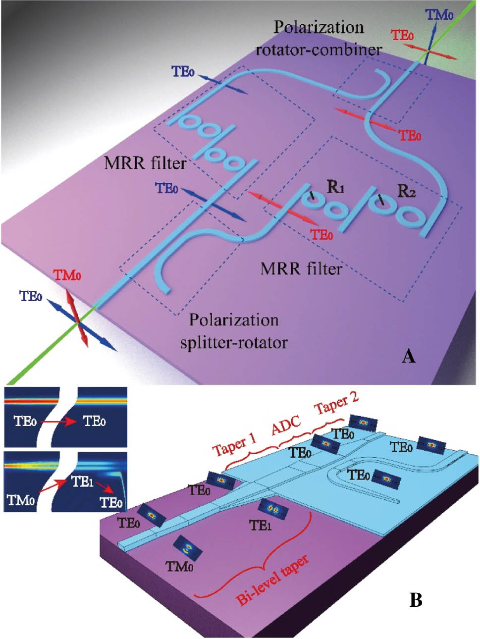
Schematic of the proposed polarization-independent tunable optical filter.
(A) The wavelength filtering part with PSR and PRC. (B) The structure of the polarization manipulation part.
As shown in Figure 2, two stages of second-order MRRs with different radii (R1 and R2) are serially cascaded. Each stage has a flat-top response with specially designed gap spacings (G0, G1, and G2). Figure 3 schematically illustrates the principle of fine adjustment of the 3 dB bandwidth. When the two passbands of the two stages are exactly aligned at a certain wavelength (see Figure 3A and B), the 3 dB bandwidth of the whole device reaches its maximum (see Figure 3C). When there is a slight misalignment between them (see Figure 3D and E), the 3 dB bandwidth of the whole device is slightly reduced (see Figure 3F). Thus, the 3 dB bandwidth is adjusted through the intentional offset between the two passbands of the two stages.

Serially cascaded second-order MRRs with different radii.
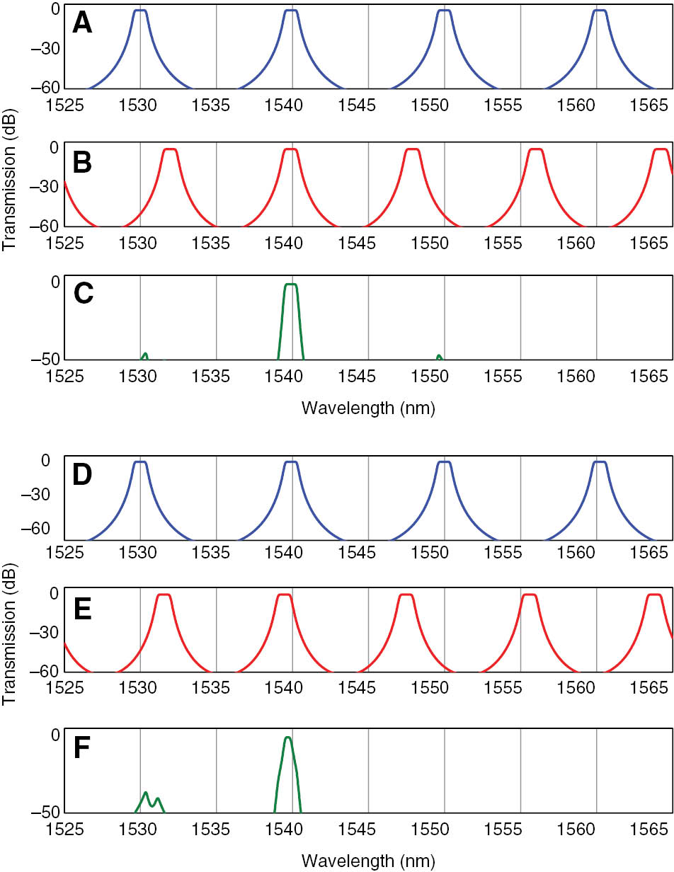
Illustration of the principle for fine adjustment of the 3 dB bandwidth.
(A–C) The 3 dB bandwidth reaches its maximum when the two stages are exactly aligned. (D–F) The 3 dB bandwidth is slightly reduced when the two stages are slightly misaligned.
The principle for the tuning of the central wavelength is illustrated in Figure 4. For example, the passbands from the two stages are aligned at 1535 nm to obtain a passband there (see Figure 4A–C). We denote the resonance orders of these two passbands at 1535 nm as m and n (see Figure 4A and B). If the location of the overall passband needs to be slightly shifted, we can just slightly change the driving signals applied to the four ring cavities. In other words, the resonance orders of the two passbands to be aligned are not changed. However, if the central wavelength needs to be greatly shifted (i.e. larger than the FSR of the first stage), then we will rely on passbands with different resonance orders. In this way, it will greatly reduce the tuning power and thus increase the tuning range. Figure 4D–F shows such an example. The target central wavelength is 1550 nm. If we rely on the two passbands with resonance orders of m and n in Figure 4A and B, we need to tune 15 nm. Instead, we can tune the nearest passband adjacent to 1550 nm, i.e. tune the passbands with resonance orders of m+1 in Figure 4A and n+1 in Figure 4B. Thus, the tuning ranges for both stages are within their respective FSRs.

Principle for the tuning of the central wavelength.
(A–C) Two passbands with the resonance order of m and n are aligned at 1535 nm and (D–F) two passbands with the resonance order of m+1 and n+1 are aligned at 1550 nm.
It should be noted that the device will show better performance (i.e. box-like response with higher roll-off rate) with a higher order (i.e. with more ring cavities in each stage of Figure 2). However, the accompanying problems include the precise fabrication control of more gap spacings and the independent tuning of more cavities. Therefore, as a proof of concept, here we just use second-order MRR as the building block. The flat-top condition of a second-order MRR is well known [44], [45], [46]. As shown in Figure 2, the gap spacing between the ring cavity and the straight waveguide G0 is chosen to be 200 nm in both stages, which is mainly limited by the fabrication accuracy. According to the flat-top condition and the 3D finite-difference time-domain (FDTD) simulations, the gap spacings between the two ring cavities in the two stages are chosen to be G1=375 nm and G2=350 nm, respectively.
The critical design for Vernier effect-based device is the choosing of radii. The FSRs of the two stages are
The ng in Eq. (1) is the group index of the ring waveguide constituting the ring cavity. Here, we assume that they are equal for ring waveguides with similar radii. The FSR of the cascaded structure is
Here, the two integer numbers m and n are mutually prime. The FSR can be further derived as [47]
We can infer from Eq. (3) that the closer the two radii are, the larger the overall FSR is. This is because close radii will result in close FSRs for the two stages and thus a small denominator in Eq. (3), whereas in practice the passbands of the two stages have spectral profiles not infinitely narrow (see Figures 3 and 4). This indicates that the radii cannot be too close. Otherwise, the side passbands other than the two we want to align will overlap with each other, resulting in lower side-passband suppression. Here, we choose the two radii to be 7 and 10 μm, respectively. Thus, the integer numbers m and n are 7 and 10 in Eq. (2), respectively, for the two stages. It means that the overall FSR will be 7 and 10 times larger than the FSRs of the two stages, respectively. The FSR of 7 and 10 μm MRRs are ~13.7 and ~9.6 nm if we use a wavelength of 1550 nm and assume a group index of 4.0 for SOI waveguides in Eq. (1). Then, according to Eq. (2), the overall FSR of the cascading structure is ~100 nm (i.e. 7×13.7 and 10×9.6 nm). It should be noted that the spectra shown in Figures 3 and 4 do not correspond to the responses of 7 and 10 μm MRRs. They are just arbitrary chosen spectra for the sake of principle illustration.
3 Fabrication and experimental results
The device is fabricated on an 8-inch (20.3 cm) SOI wafer. The thicknesses of the top silicon and the buried oxide layer are 220 nm and 2 μm, respectively. Deep ultraviolet photolithography using 193 nm scanner followed by reactive-ion etching (RIE) is employed to form the silicon waveguide. The waveguide is 400 nm in width, 220 nm in height, and 70 nm in slab thickness. As the cladding layer, a 1.5-μm-thick silica layer is deposited by the plasma-enhanced chemical vapor deposition. Then, titanium nitride with a thickness of 120 nm is sputtered on the cladding layer and Ω-shaped heaters are formed on top of the ring cavities. Via holes are etched by RIE after another 300-nm-thick silica layer. Then, an aluminum layer is sputtered and etched to form wires and pads. The last two steps are the deep trench forming via the inductively coupled plasma etching and chip dicing.
Figure 5 shows the microscope images of the fabricated device, which is about 0.55×2.5 mm in effective footprint. To characterize each stage independently, there are five input ports and five output ports (see Figure 5A). The spaces between these ports are designed to be 127 μm to facilitate the coupling and packaging with fiber arrays. The functions of different combinations of the input and output ports are summarized in Table 1.

Microscope images of fabricated device and the two MRR filters.
(A) The fabricated device with all components including the edge couplers. (B) The two MRR filters, each composed of two cascaded second-order MRRs.
Functions of different combinations of input and output ports.
| Input port | Output port | Function |
|---|---|---|
| Input 1 | Output 1 | Drop-port response of the second stage of the upper MRR filter |
| Input 2 | Output 2 | Drop-port response of the first stage of the upper MRR filter |
| Input 4 | Output 4 | Drop-port response of the first stage of the lower MRR filter |
| Input 5 | Output 5 | Drop-port response of second stage of the lower MRR filter |
| Input 3 | Output 3 | Overall response of the structure at the output of PRC |
According to the principle introduced above, the performance of the cascaded structure relies on the performances of each stage. We use an amplified spontaneous emission (ASE) source, a polarization controller (PC), and an optical spectrum analyzer to measure the transmission spectra. We use single-mode lensed fibers with a spot diameter of 5 μm to couple light in and out of the SOI chip. A PC (Agilent Technologies Polarization Controller 8169A) is used to select and change the polarization mode. According to Table 1, we tune the drop-port responses of the first and second stages of the upper and lower MRR filter, respectively, to have a passband at 1545.5 nm. Then, we measure the overall response of the device with light launching from input port 3 to output port 3 (see Figure 5a). The optical path includes the PSR, the two MRR filters, and the PRC. We randomly set the PC parameters with a large range to check the polarization-dependent performance of the device. The results are shown in Figure 6. We can find that the transmission spectra show negligible difference as the polarization state of the input light changes. We can note that the PDL is negligible. This is because, although the edge coupler and the polarization manipulation parts are not polarization independent, we rotate each of the TE and TM modes once. This will balance all the PDL in the device.

Normalized transmission spectra at four random polarization states.
Next, we will show the experimental results on the 3 dB bandwidth adjustment and take the upper MRR filters as an example. First, we tune the voltages applied to the two ring cavities in the first stage at λ=1549.7 nm until it shows a box-like spectrum and has minimal IL at the drop port (see Figure 7A). Then, we measure the drop-port response of the second stage and find the two voltages resulting in box-like spectrum (see Figure 7B). Finally, we change the input and output ports to measure the overall response of the upper MRR filter and tune the four voltages simultaneously. The resulting spectrum is shown in Figure 7C with an obvious Vernier effect. Figure 7D shows the results of 3 dB bandwidth adjustment from 37.5 to 100 GHz with a step of 12.5 GHz via misalignment of the two stages (i.e. by adjusting the four voltages). It should be noted that all the transmission spectra are normalized to the spectrum of the ASE source. The overall IL varies from −5.44 dB for 37.5 GHz bandwidth to −7.89 dB for 100 GHz bandwidth. The extinction ratio stays about 40 dB. The variation of the IL is due to the fact that the spectra of the two stages are not really flat-top. The overall IL contains fiber-chip coupling loss at the two facets, straight waveguide transmission loss, and the loss in ring cavities as well at the coupling regions. As the loss for straight SOI waveguide is approximately 3 dB/cm and the length of wavelength is about 2.5 mm, the on-chip transmission loss is about −0.75 dB. In consideration of the additional loss in ring cavities, the fiber-chip coupling loss is about −2 dB/facet, which can be further improved using a 3D taper [48]. Thus, we can estimate that the overall IL for the polarization manipulation structures is about −0.7 dB.

The experimental results of the 3 dB bandwidth adjustment.
Normalized transmission spectra of the (A) first stage, (B) second stage, and (C) cascaded structure and (D) tuning of 3dB bandwidth from 37.5 to 100 GHz with a step of 12.5 GHz.
The intrinsic quality factor and coupling coefficients are the important characteristic parameters for the device performance. Although there are no specific structures on our chip to measure them, we can calculate or estimate them based on theoretical models [49], [50], [51], numerical simulations, or experimental results. According to the formulas presented in Refs. [49], [50], [51], the intrinsic quality factor is more than 104 for a propagation loss of 10 dB/cm in the ring cavities. We calculate the coupling coefficients of the four coupling regions with 3D FDTD simulations. For the 7 μm second-order MRR, the bus-ring and ring-ring field coupling coefficients are 0.44 and 0.18, respectively; for the 10 μm second-order MRR, the bus-ring and ring-ring field coupling coefficients are 0.50 and 0.20, respectively.
The FSRs of the first and second stages are 13.6 and 9.6 nm, respectively (see Figure 7A and B). We can see in Figure 7C that the FSR of the cascaded structure is larger than 40 nm. We further measure the transmission spectra of the device in a wider range (1400–1600 nm). We use a supercontinuum fiber laser as the source, which has a much broader band than the ASE source. The experimental results are shown in Figure 8, showing an FSR of 90 nm. The side-passband suppression is about 15 dB, which can be further optimized using different radii or engineering the dispersion of the ring waveguides with different dimensions. The tuning of the central wavelength is also shown in Figure 8. We tune the central wavelength from 1460 to 1550 nm using the principle illustrated in Figure 4, with a tuning efficiency of 0.09 nm/mW. This efficiency is relatively low due to the need of simultaneous driving of the four heaters, which can be further optimized using suspended structures [52], [53]. Although we only show discrete tuning with a step of 30 nm in Figure 8, the device can be continuously tuned by finely changing the voltages applied to the ring cavities.

The experiment results of the tuning the central wavelength.
Transmission spectra located at different resonance wavelengths by thermal tuning at (A) λ0=1460 nm, (B) λ0=1490 nm, (C) λ0=1520 nm, and (D) λ0=1550 nm.
It can be noted that the upper and lower MRR filters have identical wavelength filtering function. Thus, the device shown in Figure 1 can be simplified using only one MRR filter [54], [55]. In other words, the two branches of light can be filtered by the same cascaded second-order MRRs. This will save half of the device footprint and reduce the tuning complexity and power consumption by half. We will investigate this scheme in our further work.
4 Conclusion
We have proposed and demonstrated a polarization-independent tunable optical filter with variable 3 dB bandwidth based on SOI waveguides. We use a PSR and a PRC based on adiabatic tapers and ADCs to achieve polarization-independent operation. We adjust the 3 dB bandwidth through the intentional misalignment of the two passbands. We tune the central wavelength of the filter by synchronous tuning of two stages of second-order MRR filters. We fabricate such an optical filter using 193 nm photolithography, with all the four ring cavities tunable independently. We verify the polarization-independent operation with inputs having random polarization states. The 3 dB bandwidth is adjusted from 37.5 to 100 GHz with a step of 12.5 GHz, with the IL varying from −5.4 to −7.9 dB. The FSR of the fabricated device is measured to be about 90 nm. We show the tuning of the central wavelength from 1460 to 1550 nm. The performance of the devices can be further optimized using MRR with higher order. Automatic resonance alignment of high-order MRRs can be employed to facilitate the alignments [56], [57]. This kind of optical filter can be employed to construct gridless ROADM, which is an important subsystem in future agile optical networks.
Funding: National Key R&D Program of China (2016YFB0402501).
References
[1] Ding Y, Pu M, Liu L, et al. Bandwidth and wavelength-tunable optical bandpass filter based on silicon microring-MZI structure. Opt Express 2011;19:6462–70.10.1364/OE.19.006462Search in Google Scholar PubMed
[2] Sun X, Zhou L, Xie J, et al. Tunable silicon Fabry-Perot comb filters formed by Sagnac loop mirrors. Opt Lett 2013;38:567–9.10.1364/OL.38.000567Search in Google Scholar PubMed
[3] Dong J, Liu L, Gao D, et al. Compact notch microwave photonic filters using on-chip integrated microring resonators. IEEE Photon J 2013;5:5500307.10.1109/JPHOT.2013.2245883Search in Google Scholar
[4] Qian L, Zhang D, Dai B, et al. Electrically driving bandwidth tunable guided-mode resonance filter based on a twisted nematic liquid rotator. Opt Lett 2015;5:713–6.10.1364/OL.40.000713Search in Google Scholar
[5] St-Yves J, Bahrami H, Jean P, LaRochelle S, Shi W. Widely bandwidth-tunable silicon filter with an unlimited free-spectral range. Opt Lett 2015;40:5471–4.10.1364/OL.40.005471Search in Google Scholar PubMed
[6] Kim SH, Fostand CG. Tunable narrow-band thin film waveguide grating filters. IEEE J Quantum Electron 1949;QE-15:1405–8.10.1109/JQE.1979.1069936Search in Google Scholar
[7] Sadot D, Boimovich E. Tunable optical filters for dense WDM networks. IEEE Commun 1998;36:50–5.10.1109/35.735877Search in Google Scholar
[8] Chen L. Design of flat top bandpass filters based on symmetric multiple phase shifted long-period fiber gratings. Opt Commun 2002;205:271–6.10.1016/S0030-4018(02)01363-9Search in Google Scholar
[9] Hohlfeld D, Zappe H. An all-dielectric tunable optical filter based on the thermo-optic effect. J Opt A Pure Appl 2004;6:504–11.10.1088/1464-4258/6/6/002Search in Google Scholar
[10] Ong JR, Kumar R, Mookherjea S. Ultra-high-contrast and tunable-bandwidth filter using cascaded high-order silicon microring filters. IEEE Photon Technol Lett 2013;25:1543–6.10.1109/LPT.2013.2267539Search in Google Scholar
[11] Liao S, Ding Y, Peucheret C, Yang T, Dong J, Zhang X. Integrated programmable photonic filter on the silicon-on-insulator platform. Opt Express 2014;22:31993–8.10.1364/OE.22.031993Search in Google Scholar PubMed
[12] Orlandi P, Morichetti F, Strain MJ, Sorel M, Bassi P, Melloni A. Photonic integrated filter with widely tunable bandwidth. J Lightwave Technol 2014;32:897–907.10.1109/JLT.2013.2294345Search in Google Scholar
[13] Jiang J, Qiu H, Wang G, et al. Broadband tunable filter based on the loop of multimode Bragg grating. Opt Express 2018;26:559–66.10.1364/OE.26.000559Search in Google Scholar PubMed
[14] Dai D. Highly sensitive digital optical sensor based on cascaded high-Q ring-resonators. Opt Express 2009;17:23817–22.10.1364/OE.17.023817Search in Google Scholar PubMed
[15] Claes T, Bogaerts W, Bienstman P. Experimental characterization of a silicon photonic biosensor consisting of two cascaded ring resonators based on the Vernier-effect and introduction of a curve fitting method for an improved detection limit. Opt Express 2010;18:22747–61.10.1364/OE.18.022747Search in Google Scholar PubMed
[16] Choi SJ, Peng Z, Yang Q, Dapkus PD. Tunable narrow linewidth all-buried hetero structure ring resonator filters using Vernier effects. IEEE Photon Technol Lett 2005;17:106–8.10.1109/LPT.2004.838626Search in Google Scholar
[17] Park J, Lee T, Lee D, Kim S, Hwang W, Chung Y. Widely tunable coupled-ring-reflector filter based on planar polymer waveguide. IEEE Photon Technol Lett 2008;20:988–90.10.1109/LPT.2008.923548Search in Google Scholar
[18] Ren G, Cao T, Chen S. Design and analysis of a cascaded microring resonator-based thermo-optical tunable filter with ultralarge free spectrum range and low power consumption. Opt Eng 2011;50:074601–16.10.1117/1.3602879Search in Google Scholar
[19] Radosavljevic S, Beneitez NT, Katumba A, et al. Mid-infrared Vernier racetrack resonator tunable filter implemented on a germanium on SOI waveguide platform. Opt Mater Express 2018;8:824–35.10.1364/OME.8.000824Search in Google Scholar
[20] Zhou L, Zhang X, Lu L, Chen J. Tunable Vernier microring optical filters with p-i-p type microheaters. IEEE Photonics J 2013;5:6601211.10.1109/JPHOT.2013.2271901Search in Google Scholar
[21] Yanagase Y, Suzuki S, Kokubun Y, Chu ST. Box-like filter response and expansion of FSR by a vertically triple coupled microring resonator filter. J Lightwave Technol 2002;20:1525–9.10.1109/JLT.2002.800296Search in Google Scholar
[22] Boeck R, Flueckiger J, Chrostowski L, Jaeger NA. Experimental performance of DWDM quadruple Vernier racetrack resonators. Opt Express 2013;21:9103–12.10.1364/OE.21.009103Search in Google Scholar PubMed
[23] Dai D, Liu L, Gao S, Xu D, He S. Polarization management for silicon photonic integrated circuits. Laser Photon Rev 2013;3:303–28.10.1002/lpor.201200023Search in Google Scholar
[24] Barwicz T, Watts M, Popovic M, et al. Polarization-transparent microphotonic devices in the strong confinement limit. Nat Photonics 2007;1:57–60.10.1038/nphoton.2006.41Search in Google Scholar
[25] Wang Z, Dai D. Ultrasmall Si-nanowire-based polarization rotator. J Opt Soc Am B Opt Phys 2008;25:747–53.10.1364/JOSAB.25.000747Search in Google Scholar
[26] Hosseini A, Rahimi S, Xu X, Kwong D, Covey J, Chen RT. Ultracompact and fabrication-tolerant integrated polarization splitter. Opt Lett 2011;36:4047–9.10.1364/OL.36.004047Search in Google Scholar PubMed
[27] Dai D, Wang Z, Bowers JE. Ultrashort broadband polarization beam splitter based on an asymmetrical directional coupler. Opt Lett 2011;36:2590–2.10.1364/OL.36.002590Search in Google Scholar PubMed
[28] Dai D, Wang Z, Peters J, Bowers JE. Compact polarization beam splitter using an asymmetrical Mach-Zehnder interferometer based on silicon-on-insulator waveguides. IEEE Photon Technol Lett 2012;24:673–5.10.1109/LPT.2012.2184530Search in Google Scholar
[29] Yun H, Chen Z, Wang Y, et al. Polarization-rotating, Bragg-grating filters on silicon-on-insulator strip waveguides using asymmetric periodic corner corrugations. Opt Lett 2015;40:5578–81.10.1364/OL.40.005578Search in Google Scholar PubMed
[30] Qiu H, Su Y, Yu P, Hu T, Yang J, Jiang X. Compact polarization splitter based on silicon grating-assisted couplers. Opt Lett 2015;40:1885–7.10.1364/OL.40.001885Search in Google Scholar PubMed
[31] Hu T, Qiu H, Zhang Z, et al. A compact ultrabroadband polarization beam splitter utilizing a hybrid plasmonic Y-branch. IEEE Photonics J 2016;8:1–9.10.1109/JPHOT.2016.2585113Search in Google Scholar
[32] Errando-Herranz C, Das S, Gylfason KB. Suspended polarization beam splitter on silicon-on-insulator. Opt Express 2018;26:2675–81.10.1364/OE.26.002675Search in Google Scholar PubMed
[33] Dai D, Bowers JE. Novel concept for ultracompact polarization splitter-rotator based on silicon nanowires. Opt Express 2011;19:10940–9.10.1364/OE.19.010940Search in Google Scholar PubMed
[34] Guan H, Novack A, Streshinsky M, et al. CMOS-compatible highly efficient polarization splitter and rotator based on a double-etched directional coupler. Opt Express 2014;22:2489–96.10.1364/OE.22.002489Search in Google Scholar PubMed
[35] Wang J, Niu B, Sheng Z, et al. Design of a SiO2 top-cladding and compact polarization splitter-rotator based on a rib directional coupler. Opt Express 2014;22:4137–43.10.1364/OE.22.004137Search in Google Scholar PubMed
[36] Sacher WD, Barwicz T, Taylor BJF, Poon JKS. Polarization rotator-splitters in standard active silicon photonics platforms. Opt Express 2014;22:3777–86.10.1364/OE.22.003777Search in Google Scholar PubMed
[37] Hu T, Rouifed MS, Qiu H, et al. A polarization splitter and rotator based on a partially etched grating-assisted coupler. IEEE Photon Technol Lett 2016;28:911–4.10.1109/LPT.2016.2517196Search in Google Scholar
[38] Little BE, Chu ST, Absil PP, et al. Very high order microring resonator filters for WDM applications. IEEE Photon Technol Lett 2004;16:2263–5.10.1109/LPT.2004.834525Search in Google Scholar
[39] Xiao S, Khan MH, Shen H, Qi M. A highly compact third-order silicon microring add-drop filter with a very large free spectral range a flat passband and a low delay dispersion. Opt Express 2007;15:14765–71.10.1364/OE.15.014765Search in Google Scholar PubMed
[40] Hu T, Wang W, Qiu C, et al. Thermally tunable filters based on third-order microring resonators for WDM applications. IEEE Photon Technol Lett 2012;24:524–6.10.1109/LPT.2012.2182988Search in Google Scholar
[41] Luo X, Song J, Feng S, et al. Silicon high-order coupled microring based electro-optical switches for on-chip optical interconnects. IEEE Photon Technol Lett 2012;24:821–3.10.1109/LPT.2012.2188829Search in Google Scholar
[42] Chen P, Chen S, Guan X, Shi Y, Dai D. High-order microring resonators with bent couplers for a box-like filter response. Opt Lett 2014;39:6304–7.10.1364/OL.39.006304Search in Google Scholar PubMed
[43] Dai D, Tang Y, Bowers JE. Mode conversion in tapered submicron silicon ridge optical waveguides. Opt Express 2012;20:13425–39.10.1364/OE.20.013425Search in Google Scholar PubMed
[44] Deng L, Li D, Liu Z, Meng Y, Guo X, Tian Y. Tunable optical filter using second-order micro-ring resonator. Chin Phys B 2017;26:024209-1–4.10.1088/1674-1056/26/2/024209Search in Google Scholar
[45] Manganelli CL, Pintus P, Gambini F, et al. Large-FSR thermally tunable double-ring filters for WDM applications in silicon photonics. IEEE Photonics 2017;9:1–10.10.1109/JPHOT.2017.2662480Search in Google Scholar
[46] Zhang L, Zhao H, Wang H, et al. Cascading second-order microring resonators for a box-like filter response. J Lightwave Technol 2017;35:5347–60.10.1109/JLT.2017.2775658Search in Google Scholar
[47] Rabus DG. Integrated ring resonators. Springer series in optical sciences. Berlin/Heidelberg/New York, Springer, 2007.Search in Google Scholar
[48] Fang Q, Song J, Tu X, et al. Low loss fiber-to-waveguide converter with a 3D functional taper for silicon photonics. IEEE Photon Technol Lett 2016;28:2533–6.10.1109/LPT.2016.2602366Search in Google Scholar
[49] Rabiei P, Steier WH, Zhang C, Dalton LR. Polymer micro-ring filters and modulators. J Lightwave Technol 2002;20:1968–75.10.1109/JLT.2002.803058Search in Google Scholar
[50] Dai D, Shi Y, He S, Wosinski L, Thylen L. Silicon hybrid plasmonic submicron-donut resonator with pure dielectric access waveguides. Opt Express 2011;19:23671–82.10.1364/OE.19.023671Search in Google Scholar PubMed
[51] Zhang Y, Hu X, Chen D, et al. Design and demonstration of ultra-high-Q silicon microring resonator based on a multi-mode ridge waveguide. Opt Lett 2018;43:1586–9.10.1364/OL.43.001586Search in Google Scholar PubMed
[52] Dong P, Qian W, Liang H, et al. 1×4 Reconfigurable demultiplexing filter based on free-standing silicon racetrack resonators. Opt Express 2010;18:24504–9.10.1364/OE.18.024504Search in Google Scholar PubMed
[53] Dong P, Feng N, Feng D, et al. GHz-bandwidth optical filters based on high-order silicon ring resonators. Opt Express 2010;18:23784–9.10.1364/OE.18.023784Search in Google Scholar PubMed
[54] Li C, Song JH, Zhang J, et al. Silicon polarization independent microring resonator-based optical tunable filter circuit with fiber assembly. Opt Express 2011;19:15429–37.10.1364/OE.19.015429Search in Google Scholar PubMed
[55] Zhang J, Zhang H, Chen S, Yu M, Lo GQ, Kwong DL. A tunable polarization diversity silicon photonics filter. Opt Express 2011;19:13063–72.10.1364/OE.19.013063Search in Google Scholar PubMed
[56] Mak JCC, Sacher WD, Xue T, et al. Automatic resonance alignment of high-order microring filters. IEEE J Quantum Electron 2015;51:1–11.10.1109/JQE.2015.2479939Search in Google Scholar
[57] Mak JCC, Bois A, Poon JK. Programmable multiring Butterworth filters with automated resonance and coupling tuning. IEEE J Sel Top Quantum Electron 2016;22:232–40.10.1109/JSTQE.2016.2540618Search in Google Scholar
© 2018 Lei Zhang and Lin Yang et al., published by De Gruyter, Berlin/Boston
This work is licensed under the Creative Commons Attribution-NonCommercial-NoDerivatives 4.0 License.
Articles in the same Issue
- Review articles
- Programmable multifunctional integrated nanophotonics
- Photonics of DNA/ruthenium(II) complexes
- From nanoscopic to macroscopic photo-driven motion in azobenzene-containing materials
- Fluorescent nanodiamonds: past, present, and future
- Research articles
- A scatterer-assisted whispering-gallery-mode microprobe
- Power-efficient generation of two-octave mid-IR frequency combs in a germanium microresonator
- Polarization-independent tunable optical filter with variable bandwidth based on silicon-on-insulator waveguides