Engineering of superconductors and superconducting devices using artificial pinning sites
-
Roger Wördenweber


Abstract
Vortex matter in superconducting films and devices is not only an interesting topic for basic research but plays a substantial role in the applications of superconductivity in general. We demonstrate, that in most electronic applications, magnetic flux penetrates the superconductor and affects the performance of superconducting devices. Therefore, vortex manipulation turns out to be a useful tool to avoid degradation of superconducting device properties. Moreover, it can also be used to analyze and understand novel and interesting physical properties and develop new concepts for superconductor applications. In this review, various concepts for vortex manipulation are sketched. For example, the use of micro- and nanopatterns (especially, antidots) for guiding and trapping of vortices in superconducting films and thin film devices is discussed and experimental evidence of their vortex guidance and vortex trapping by various arrangements of antidots is given. We demonstrate, that the vortex state of matter is very important in applications of superconductivity. A better understanding does not only lead to an improvement of the performance of superconductor components, such as reduced noise, better power handling capability, or improved reliability, it also promises deeper insight into the basic physics of vortices and vortex matter.
1 Introduction
With only a few exceptions, the electronic properties of type-II superconductors and the performance of superconducting devices are predominantly determined by the action of magnetic flux, i.e., the motion of magnetic flux lines (vortices). Magnetic flux penetrates the superconductor in the form of flux lines (vortices) that contain the smallest possible amount of magnetic flux, the magnetic flux quantum
An applied current induces a Lorentz force
The motion of individual vortices typically leads to a degradation of the performance of superconducting electronic devices. This is illustrated in the second row of figures in Figure 1 for the case of a superconducting magnetometer, the SQUID (superconducting quantum interference device). The motion of a single vortex leads to a telegraph-type noise in the sensor. The action of many vortices creates the typical 1/f noise in these sensors. Similar effects are known for other types of superconducting electronics. For instance in passive devices (e.g., filters) or active devices (e.g., rapid single-flux quantum logic, RSFQ) vortex motion leads to a reduction of the power-handling capability or enhances the bit error rate, respectively.
In contrast to the previous examples, the motion of the vortices can also be used for magnetic field or signal management (ranging from flux guides, flux focusers, ratchets, filters) or data handling (RSFQ-type devices). This direction is generally called fluxonics.
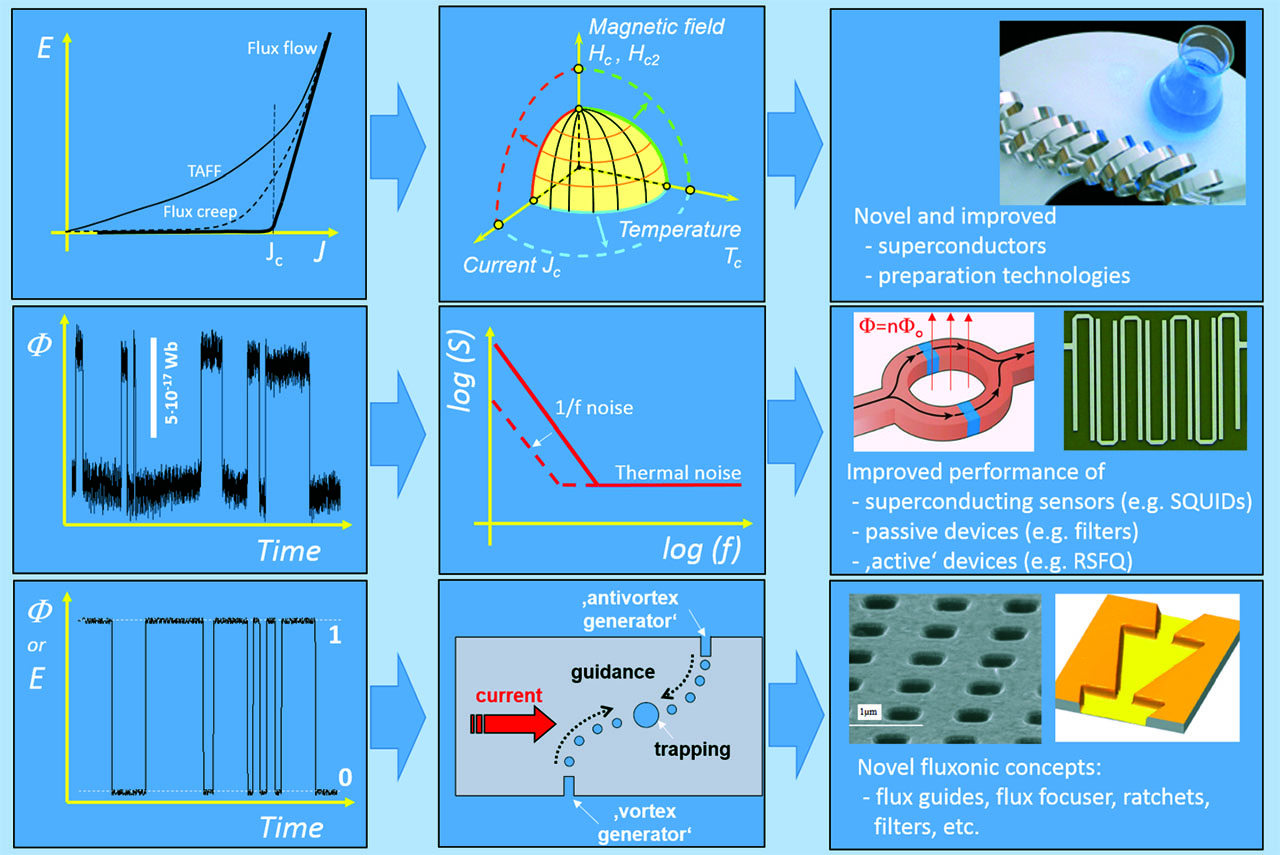
Schematic sketches of the different scenarios of the impact of vortex motion on technological superconducting and superconducting devices. (i) (Top row, from left to right) The nonlinear current-voltage characteristic demonstrates the onset of flux flow at the critical current density
All three scenarios lead to one solution, the systematic manipulation of vortices which includes the pinning and/or the guided motion of vortices. This manipulation of vortices might be achieved by naturally grown defects. However, it is evident that artificial defects present not only a crucial alternative to natural pinning sites; in quite a number of concepts they are absolutely necessary to achieve the desired goal (e.g., in the case of fluxonic devices).
In the following sections, I will briefly introduce different types of artificial defects, basic aspects of their pinning interaction, the different possible types of flux motion between well-separated pinning sites, and the basic demonstration of vortex-pin interaction and vortex guidance, before we move to aspects of artificial pinning sites in different applications like SQUIDs, passive devices, or fluxonics.
2 Artificial pinning sites
There exist a large number of artificial pinning sites. In principle, any kind of modification of the superconducting material has an impact on the flux pinning potential of the superconductor. The question is whether the impact is large enough and suitable for the envisioned experiment or application. For the right choice of defect type the consideration of different possible classifications of artificial pinning sites is helpful:
Pinning interaction and pinning strength: There exist two essentially different types of pinning interactions, which are the magnetic interaction and the core interaction. The magnetic interaction is essentially determined by the magnetic field gradient in the superconductor (characterized by the penetration length
Size: The typical size of a pinning site based on core interaction (e.g.,
Orientation and dimension: The ‘classical’ pinning site is a point defect, which can be considered to be a 0D pinning site. 1D pinning sites can be generated for instance by irradiation, whereas typical 2D pinning sites are represented by all types of surfaces including the surfaces of the sample itself, surfaces of extended defects, interfaces, and even modulations of the superconductivity in highly anisotropic superconductors. The latter leads to so-called intrinsic pinning for instance observed in ceramic high-
Connectivity: Connected superconducting areas with locally tailored electrical properties (mainly ‘channels for vortex motion’) are used mainly for vortex guidance. Nonsimply connected micro- or nanostructures will cause a long-range electronic or magnetic interaction between vortex and artificial structure. Generally, the flux pinning and flux transport is different for both arrangements.
Preparation: There exist a large variety of preparation methods for artificial defects. During the formation of the superconducting material, deviations from the stoichiometry, doping, or addition of other phases or nanoparticles automatically create defects which are usually statistically distributed. These in situ methods are used, for instance, for the improvement of the critical current density in large-scale applications like the fabrication of superconducting cables and coated conductors. However, after preparation of the material, defects can also be introduced by many ex situ techniques. Irradiation with energetic particles (ions, protons,
Reconfigurability: Typically, pinning sites are not reconfigurable. This also holds for artificial defects. Nevertheless, there have been attempts to produce reconfigurable defects for instance using soft magnetic dots (with switchable magnetization), ferroelectric top layers (with reconfigurable polarization), or locally reconfigurable stoichiometry (e.g., local modification of the oxygen content in ceramic high-
From this list, it is obvious that one can and should choose the respective type of defect according to the needs of the experiment or the application. Nevertheless, a number of particularly interesting patterns and defect types are briefly described below.
![Figure 2: SEM images of artificial defects ranging from BaZrO3$$\mathrm{BaZrO_{3}}$$ nanoparticles, antidots, or heavy-ion patterned channels in YBa2Cu3O7−δ$$\mathrm{YBa_{2}Cu_{3}O}_{\mathrm{7-\delta}}$$ thin films [4, 5, 6, 7, 8] to patterned channels in NbN/NbGe bilayer [2, 3, 9].](/document/doi/10.1515/psr-2017-8000/asset/graphic/j_psr-2017-8000_figure2.jpg)
Artificial channels: The most obvious concept to provide a controlled vortex motion (the so-called guided vortex motion) is given by the patterning of narrow channels into superconducting material. This can be done by etching channel structures into a single layer leading to modification of the pinning force due to thickness variation, local modification of the superconducting properties (for instance via heavy-ion lithography or antidots), or by combining two layers of superconducting material with different pinning properties.
Combination of weak and strong pinning material: An intriguing example of easy vortex flow channels consists of a weak-pinning bottom layer (e.g., amorphous NbGe) combined with a strong-pinning top layer (e.g., NbN), into which the small channels are etched (see Figure 2) [2, 3]. Since the pinning force in the channel is extremely weak, the vortices in the channels predominantly experience vortex-vortex interaction with the row of the strongly pinned vortices at the edge of the channel within the NbN. The commensurability between the vortex lattice with a field-dependent lattice parameter
However, rather more complex channel patterns can be used. An example of a ratchet system using the same system (weak-pinning a-NbGe in combination with a strong-pinning and patterned NbN top-layer) is shown in Figure 1 [10]. Using an asymmetric, ‘fyke-like’ pattern, the vortex motion is not only guided, it can be rectified and, thus, create a fluxonic ratchet.
Similar structures are possible for high-
Heavy-ion lithography: Ion irradiation of HTS (high-temperature superconducting) films offers a unique possibility to create a wide range of different defects and to tailor the electrical and superconducting properties [1]. Depending on the species of ions used during the irradiation, their energy and fluence, nanoscale columnar pinning centers can be created that locally enhance or diminish the pinning properties. Whereas the irradiation with relatively low fluence of high-energy heavy ions leads to an enhancement of the critical current due to the strong vortex pinning at columnar defects, relatively high fluence leads to a reduction of the critical properties. Thus, the superconducting properties can be controlled and modulated locally. The preparation of artificial channels for flux motion has been demonstrated for this technology [7].
Dots and antidots: In contrast to simply connected structures, dots and holes (antidots) offer a number of advantages for the manipulation of vortices: (i) dots or antidots of various size, properties, and shapes can be used or even combined, (ii) they can be positioned more or less at wish, even quite complex arrangements are possible, (iii) they can be used as pinning (single-flux quanta) or trapping (multiflux quanta) sites as well as for the guidance of flux, and (iv) the motion of flux between dots or antidots can be examined and used.
In contrast to other pinning defects, which have to be of the order of the size of the superconducting coherence length
commensurability effects (matching effects) between the antidot lattice and vortex lattice;
multiquanta formation in the antidots;
guided motion along rows of antidots;
visualization of vortex motion, and;
implementation of antidots in cryoelectronic devices.
Because of their unique properties, I will concentrate in this chapter on the role of antidots and their options and prospects for the manipulation of vortices. Nevertheless, most concepts can easily be used for the understanding of other types of artificial defects and their use in devices.
3 Vortex Manipulation via Antidots
In this section, basic aspects of vortex manipulation via antidots are given, including vortex-antidot interaction, multiquanta vortex formation, commensurability or matching effects, different modes of vortex motion between antidots, and vortex guidance.
3.1 Vortex-Antidot Interaction and Multiquanta Vortices
However, in contrast to the classical pinning defects, antidots represent extended (
The interaction energy between a vortex and a small insulating cylindrical cavity (analogue to an antidot) has been calculated using the London approximation [14] and an alternative approach using the analogy between a vortex close to an antidot and a charge line in an infinite dielectric close to a cylindrical cavity of different dielectric permittivity [15]. Later, the calculations were extended to arbitrarily large cavities [31]. It is demonstrated that the interaction energy is identical to the one between a vortex and the straight edge of a superconductor (Bean–Livingston barrier [32]) when the radius of the antidot goes to infinity. Although the precise form of the interaction potential between a vortex and a cylindrical antidot is slightly different in these studies [14, 15, 31], the main conclusions are identical.
On the basis of a series expansion of Bessel functions
for
The vortex-antidot interaction depends upon the magnetic flux
the pinning force per unit length depends on the radial distance between vortex and antidot and has a maximum value close to the antidot edge
i.e., the maximum vortex-antidot interaction decreases with increasing occupation number and becomes zero for
Generally, the saturation number depends upon temperature, i.e., it increases with decreasing temperature. Furthermore, a consequence of a saturation number
![Figure 3: Free energy of a vortex as a function of the radial distance from an antidot for different occupation numbers n$$n$$ of the antidot (λ=600nm$$\lambda=\mathrm{600\,nm}$$, κ=50$$\kappa=50$$, and ro=200nm$$r_{\mathrm{o}}=\mathrm{200\,nm}$$), (inset) sketch of a vortex interacting with a cylindrical cavity formed by an antidot with radius ro$$r_{\mathrm{o}}$$, and (b) reconstruction of the trapped magnetic flux distribution obtained from a magneto-optic image that was recorded at 7K$$\mathrm{7\,K}$$ in zero-field after applying a field of 1T$$\mathrm{1\,T}$$ [33]. The local field shows clear maxima at the position of the antidots (triangular lattice, dAA=10μm$$d_{AA} = {\mathrm{10\,{\mu}m}}$$, ro≈1μm$$r_{\mathrm{o}}\approx {\mathrm{1\,{\mu}m}}$$). The scale for the height of the peaks is given in numbers of trapped flux quanta.](/document/doi/10.1515/psr-2017-8000/asset/graphic/j_psr-2017-8000_figure3.jpg)
Free energy of a vortex as a function of the radial distance from an antidot for different occupation numbers
3.1.1 Matching or commensurability effect
The matching or commensurability effect represents an ideal tool to demonstrate the interaction between a regular (typically hexagonal) vortex lattice and a regular defect lattice. Furthermore, it provides a first approach to improve the flux pinning for discrete magnetic fields (matching fields).
Since the vortex lattice parameter
While periodic pinning arrays show these enhanced pinning properties for a few discrete field values, at which the vortex density and defect density are integer multiples of each other, quasiperiodic arrays represent a valuable alternative, as they have many more built-in periodicities to which the vortex lattice can be approximately commensurate [35, 36, 37]. This leads to broadened maxima of the pinning efficiency and to a reduced sensitivity of the sample properties to magnetic field variations. Therefore, quasiperiodic arrays of artificial defects represent a first option to improve flux pinning over a larger field range.
Matching effects can also be demonstrated via noise measurements. Since this automatically leads us to an important aspect of the use of strategically positioned artificial defects (see Section 4.2) an example of this demonstration is briefly described in the following.
![Figure 4: (a) Low-frequency noise spectra of a bicrystal rf-SQUID (sketch) with a square antidot lattice on top of the grain boundary of the washer for different magnetic fields [38]. M1$$\mathrm{M_{1}}$$ and M2$$\mathrm{M_{2}}$$ label two matching conditions (see sketch in [b]). The inset (a) shows a sketch of the experimental arrangement. A YBCO film with square antidot lattice (dAA$$d_{AA}$$=5μm$$\mathrm{5\,{\mu}m}$$) is mounted in flip-chip configuration on top of the grain boundary of a bicrystal rf-SQUID. One of the main axes of the antidot lattice is oriented parallel to the grain boundary. The matching fields Mi$$M_{\mathrm{i}}$$ (i=1,2$$i = 1,2$$) in the field range 450 to 900nT$$\mathrm{900\,nT}$$ are given in (b). They are calculated for different vortex configurations (see schematic sketch for i=1−3$$i=1{-}3$$ in [b]) that match the square antidot array with a periodicity of 5μm$${\mathrm{5\,{\mu}m}}$$. For details, especially about the different matching conditions, see [38].](/document/doi/10.1515/psr-2017-8000/asset/graphic/j_psr-2017-8000_figure4.jpg)
(a) Low-frequency noise spectra of a bicrystal rf-SQUID (sketch) with a square antidot lattice on top of the grain boundary of the washer for different magnetic fields [38].
In this experiment [38] a periodic array of artificial defects (YBCO film with a square lattice of antidots) is mounted in flip-chip configuration on a YBCO bicrystal rf-SQUID (see sketch in Figure 4a). Typical low-frequency noise spectra of this arrangement are given in Figure 4a. As expected, the lowest flux noise is recorded for zero magnetic field. At nonzero field, the low-frequency noise strongly depends upon the exact value of the applied magnetic field. In contrast to the standard field dependence
Later we will see that in many cases a ‘strategic’ arrangement of artificial defects is necessary to optimize the benefit from artificial defects in superconducting devices.
3.2 Guided vortex motion
Probably even more important than flux trapping is the guidance of vortices by artificial defects. Guided motion has been demonstrated in conventional weak-pinning superconductors [2, 3, 9] and HTS thin films [7] using channels prepared via patterning or heavy-ion irradiation (see also Figure 2). However, an intriguing and more flexible method of vortex guidance is provided by special arrangements of antidots, i.e., rows of antidots [33, 39].
A first basic explanation of the angular dependence of the guidance of vortices via rows of antidots is given by the
with
where the summation is performed over all possible channels of vortex motion, and
![Figure 5: Angular dependence of the Hall resistance (solid symbols) and 1-channel approximation (dashed line). The sketch illustrates the angular dependence of the Hall signal according to the n$$n$$-channel model [6], the image shows an experimental demonstration of the guidance of vortices for rows of antidotes arranged at an angle γ=−9º$$\gamma = -9\text{\degree}$$ with respect to the Lorentz force obtained via laser scanning microscopy [40].](/document/doi/10.1515/psr-2017-8000/asset/graphic/j_psr-2017-8000_figure5.jpg)
Angular dependence of the Hall resistance (solid symbols) and 1-channel approximation (dashed line). The sketch illustrates the angular dependence of the Hall signal according to the
In order to obtain a more detailed insight into the guidance of vortices via rows of antidots, resistive 6-probe dc measurements can be performed on superconducting films equipped with rows of antidots that simultaneously record the longitudinal voltage signal and the Hall signal [6, 30]. Figure 6 shows schematically the typical sample design that is suitable for simultaneous recording of the longitudinal voltage and the Hall voltage.
The longitudinal voltage (contacts
High-
![Figure 6: Demonstration of guided vortex motion via Hall measurements. (a) The Hall resistance for an unpatterned YBCO film shows the typical anomalous Hall effect (AHE), i.e., the sign inversion at temperatures just below Tc$$T_{\mathrm{c}}$$; (b) because of the tilted rows of antidots the guided motion (GM) enhances the AHE and extends the regime of negative Hall resistance to low temperatures [6]; (c) in case of a tilt angle opposing the direction of the AHE a sign inversion is visible for the current dependence of the Hall voltage for temperatures close to Tc$$T_{\mathrm{c}}$$, i.e., the direction of collective flux flow changes from GM (small current) to AHE (large current); (d) another demonstration of the change of the direction from AHE to GM is given by the longitudinal current which generates a constant flux flow perpendicular to the current (i.e., a constant absolute Hall voltage, here |VHall|=100μV$$|V_{\mathrm{Hall}}| = \mathrm{100\,{\mu}V}$$). A detailed description of the experimental details is given in the text, the sketches in the figures illustrate the arrangement of the experiment (Vx$$V_{x}$$ and Vy$$V_{y}$$ mark the longitudinal and Hall contacts, respectively, 1 and 2 are the current contacts), the orientation of the rows of antidots γ$$\gamma$$, and forces [30].](/document/doi/10.1515/psr-2017-8000/asset/graphic/j_psr-2017-8000_figure6.jpg)
Demonstration of guided vortex motion via Hall measurements. (a) The Hall resistance for an unpatterned YBCO film shows the typical anomalous Hall effect (AHE), i.e., the sign inversion at temperatures just below
If the directions of the Magnus force and the GM coincide (
If the directions of the Magnus force and the GM are opposite (
In the last example (Figure 6d) we again observe the switching from the AHE at high temperature to the GM at low temperature. In this experiment, the Hall voltage (absolute value) has been kept constant (
Generally, guidance of vortices via antidot arrangements is now well established. However, it depends in a complicated way on the relation (amplitude and direction) of the different forces and potentials acting on the vortices. The major forces to be considered are the ‘background’ pinning force of the superconductor, the vortex-antidot interaction, driving forces (e.g., Lorentz force), Magnus force, and thermal activation. Some of these interactions depend on temperature, others on their orientation direction. This can lead to switching of the direction of vortex motion as a function of temperature (see Figure 6d), current density (see Figure 6c), or orientation of antidot arrangement (see Figure 6). As a consequence, guidance of vortices strongly depends upon temperature, driving force, and geometrical arrangement of the antidots. If additionally anisotropic pinning potentials are introduced (e.g., via asymmetrically shaped antidots) preferentially directed vortex motion can be induced leading to more complex concepts of for instance ratchets, vortex diodes, or vortex filters.
3.3 Vortices at high velocity
Studies of vortex matter are predominantly focused on the limit of small driving forces and small frequencies, i.e., the onset of vortex dynamics in the limit of small vortex velocities. However, a number of superconductor applications like coated conductors, fault-current limiters, or microwave devices operate at high power levels or high frequencies and, therefore, potentially in the regime of high vortex velocities. This scenario also applies for the guided vortex motion in a superconductor equipped with an array of antidots if flux is expected to shuttle between closely spaced antidots at high frequencies. For example, in case of an antidot spacing of
In principle three different approaches to this scenario are feasible:
With increasing vortex velocity the classical Abrikosov vortices gradually start to deform. Nevertheless, they can be treated as ‘ballistic vortices’ with slightly modified properties.
At a characteristic velocity, the so-called critical velocity, the vortices abruptly change their properties [51]. This high-velocity range is often associated with a different vortex state, the so-called kinematic vortices.
Pulsed measurements of the current-voltage characteristics (IVC) on classical superconductors [54, 55] as well as HTS material [56, 57, 58] demonstrate, that scenario (i) does not apply. At a critical voltage, the IVC changes abruptly (see Figure 7). Depending on the type of measurement, the voltage switches in an S-like shape (for voltage-controlled IVCs) or jump-like (for current-controlled IVCs) from the nonlinear region of the Abrikosov flux flow below
![Figure 7: Inelastic scattering rate (a) and resulting critical vortex velocity (b) as a function of temperature for YBCO films obtained from IVC measurements via rapid current ramps (open symbols) [56] and current pulses (solid symbols) [58], respectively. The inset shows a schematic drawing of a voltage-controlled and current-controlled IVC measured up to voltages V>V∗$$V \gt V^\ast$$.](/document/doi/10.1515/psr-2017-8000/asset/graphic/j_psr-2017-8000_figure7.jpg)
Inelastic scattering rate (a) and resulting critical vortex velocity (b) as a function of temperature for YBCO films obtained from IVC measurements via rapid current ramps (open symbols) [56] and current pulses (solid symbols) [58], respectively. The inset shows a schematic drawing of a voltage-controlled and current-controlled IVC measured up to voltages
Critical velocity
On the basis of Eliashberg’s ideas on nonequilibrium effects in superconductors, Larkin and Ovchinnikov predicted that a nonequilibrium distribution and relaxation rate of the normal charge carriers (treated as quasiparticles) develops during the motion of vortices at high velocities [51]. As a result, they expected a discontinuity in the current-voltage characteristic (IVC).
According to the Larkin and Ovchinnikov theory, the viscous damping coefficient at a vortex velocity
with a critical vortex velocity
denoting the inelastic quasiparticle scattering time,
with
Phase slip
The predictions of Larkin and Ovchinnikov [51] refer to extended superconducting systems. The situation changes if vortices move in a mesoscopic system. It is known that flux transport across a narrow superconducting stripline can occur in the form of a phase slip [52, 53]. In this case the phase of the order parameter may periodically slip by 2
In contrast to the PSC, the oscillation of the order parameter may not necessarily be uniform along the PSL, it may occur in the form of propagating waves carrying the order parameter singularities across the sample. Such waves have been named kinematic vortices. They were first predicted in numerical simulations using the 2D time-dependent Ginzburg–Landau equations [65]; the experimental evidence for the existence of kinematic vortices is among others reported in [64]. As such, PSLs can be viewed as dynamically created Josephson junctions in homogeneous superconducting films. Therefore, the preservation of the macroscopic quantum interference between the two parts of the superconductor defined by the slip line represents a fingerprint of the phase-slip mechanism. However, its demonstration for instance via Shapiro steps under microwave irradiation is not trivial.
Besides their superconducting properties, the maximum vortex velocities, which differ by orders of magnitude for the different types of vortices, is of importance for experimental techniques and potential applications. The smallest velocity is observed for classical Abrikosov vortices with a typical maximum speed given by the critical velocity of
4 Artificial pinning sites in superconducting electronic devices
In this section examples of active devices and passive microwave devices will be given that illustrate the role that vortices play in superconducting devices starting with a brief motivation that demonstrates why vortices and vortex motion have to be considered for nearly all superconducting devices.
4.1 Flux penetration in superconducting electronic devices
The electronic properties of superconducting devices are usually strongly determined or affected by the presence or motion of vortices. Most superconducting devices will (or have to) operate in magnetic fields strong enough to create large densities of vortices within the device. Generally flux penetrates the superconductor for magnetic fields
followed by a collective penetration of vortices that takes place at the penetration field
These predictions are valid for superconducting devices and patterns if
(a) Critical field
The presences of vortices or their motion will lead to dissipative processes, flux noise, or local modification of the superconducting properties in these devices which, in most applications, means that the performance of the device is diminished. Because of the large anisotropy, the small coherence length and, last but not least, the elevated temperature at which the ceramic superconductors will be operated, these effects are more severe for HTS materials. Ways to avoid the impact of vortices are:
operation in perfectly shielded environments;
reduction of the structures to sizes that do not allow for vortex formation, or;
‘manipulation’ of vortex matter.
Since the first two options are in most cases (extremely) costly and/or usually technically difficult or impossible, the manipulation of vortex matter appears to be an ideal solution of this problem. This is one of the motivations for scientific studies on vortex manipulation in superconducting films. Furthermore, the manipulation of vortices is also of interest for the development of (novel) fluxonic concepts. In the following, I will sketch possible routes to improve existing superconducting devices and show concepts for possible novel devices that are based on the manipulation of vortices via artificial pinning sites.
4.2 Strategically positioned antidots in Josephson-junction-based devices
Noise reduction in SQUIDs
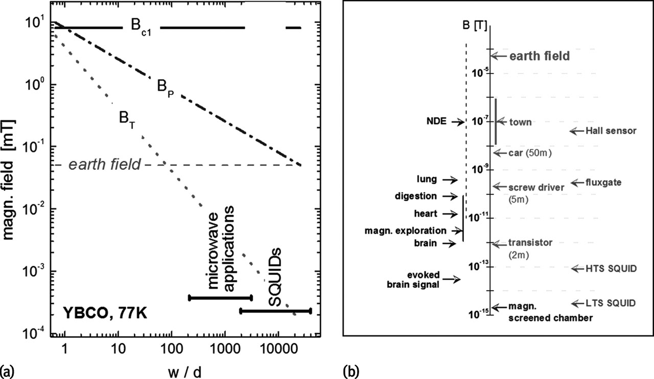
Superconducting quantum interference devices (SQUIDs) represent the most sensitive sensors of magnetic flux or other physical quantities (e.g., currents) that can be transformed into magnetic flux. They are for instance used for nondestructive testing (NDE), geomagnetic applications, biomagnetic or medical applications (e.g., magnetoencephalography). Typical magnetic signals for the different applications are shown in Figure 8. It demonstrates that the magnetic fields that have to be recorded are much smaller (in some cases orders of magnitude smaller) than the magnetic field of other sources like urban noise or even the earth. Therefore it is obvious, that magnetic flux which doesn’t stem from the measured object has to considered.
In principle, the SQUID is a deceptively simple device, consisting of (see also Figure 1) a superconducting loop with one (rf-SQUID) or two (dc-SQUID) Josephson junctions, respectively. Magnetic flux threading the superconducting loop leads to a phase difference
![Figure 9: (a) Spectral noise density for different magnetic fields measured in a HTS step-edge type rf-SQUID [11]. The lines idealize the different noise contributions, i.e., the field-dependent 1/f$$1/f$$ low-frequency noise and the field- and frequency-independent white noise. The schematic drawing sketches the geometry of rf-SQUIDs and the problem of a moving vortex in the washer. (b) Magnetic field dependencies of the integral noise (0.5 and 10Hz$$\mathrm{10\,Hz}$$) of a step-edge and bicrystal Josephson junction according to [11]. The dotted lines represent the theoretical field dependence of the low-frequency noise according to Equation (11).](/document/doi/10.1515/psr-2017-8000/asset/graphic/j_psr-2017-8000_figure9.jpg)
(a) Spectral noise density for different magnetic fields measured in a HTS step-edge type rf-SQUID [11]. The lines idealize the different noise contributions, i.e., the field-dependent
Generally, the sensitivity of SQUIDs is limited by the frequency-dependent noise level of the device. In addition to the contribution of the electronics (usually white noise), in active superconducting devices two different sources are considered to be responsible for the noise. These are the contribution of the active part of the device, which usually consists of one or more Josephson junctions, and the noise coming from the passive component, the superconducting thin film (washer, flux focuser, or flux transformer, depending on the application). The noise mechanisms in Josephson junctions are well understood [67], and a reduction of this noise contribution via simple electronic means has been successfully demonstrated [68]. The passive component (e.g., the superconducting film of the loop, washer, or flux transformer) contributes strongly to the low-frequency noise due to vortex motion in the superconducting film. A nice illustration of this contribution is given by the so-called telegraph noise that occurs when a vortex hops between two pinning sites (see Figure 1). In the case of the statistical motion of many vortices (incoherent superposition of many thermally activated microscopic fluctuators), a scaling of the spectral noise density
with
In Section 3.1.1 it was demonstrated that the low-frequency noise in SQUIDs can be manipulated via antidots. However, it can be seen in Figure 4 and it is evident from theoretical considerations, that regular arrays of antidots lead to noise reduction only at discrete values of the magnetic field (at matching fields) whereas in case of noncommensurability between the vortex and antidot lattice even an increase of the low-frequency noise is observed. Therefore it is better to use only a few, ‘strategically positioned’ antidots in the superconducting device, which trap only those vortices that attribute strongly to the low-frequency noise (e.g., vortices close to the SQUID hole) and leave the vortex lattice free to arrange itself within the device. Thus, the important issue is to allocate those strategic positions.
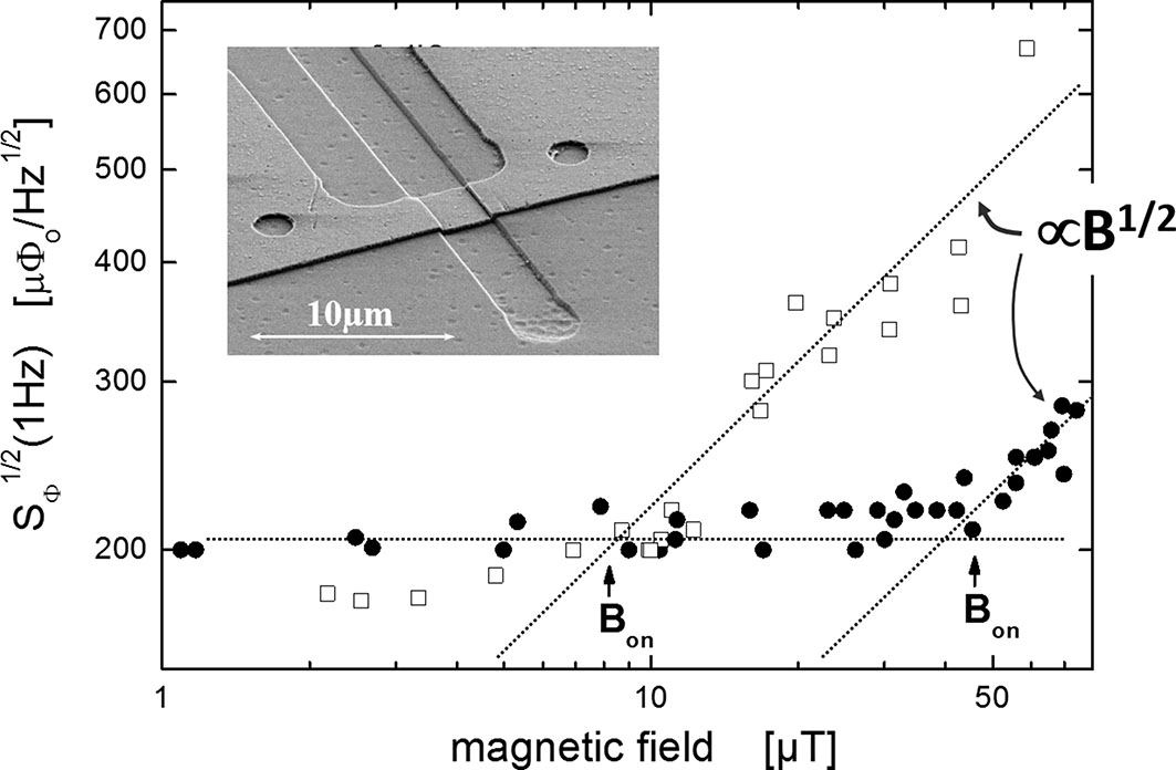
Spectral noise density at
An experimental demonstration for noise reduction via strategically positioned antidots is shown in Figure 10 [11, 12, 38]. Since the largest impact of vortex motion upon the SQUIDs flux noise is expected for vortex motion at a position close to the SQUID hole and close to the Josephson junction, two antidots are positioned on either side of the Josephson junction of an rf-SQUID (see SEM image in Figure 10). The resulting modification of the noise properties is determined in field-cooled (FC) experiments on the same SQUID without and with antidots. In these experiments, the SQUID is cooled from the normal to the superconducting state in an applied field
Abrikosov-vortex based active devices
We can invert the effect demonstrated above and utilize the impact of trapped vortices on the signal of a Josephson-type device for superconducting digital devices. Generally, Abrikosov vortices represent extremely small magnetic bits
A very nice proof of this concept is given in [70] where an Abrikosov-vortex-based random access memory (AVRAM) cell is demonstrated, in which a single vortex is used as an information bit. The basic principle and the operation is illustrated in Figure 11. The AVRAM simply consists of a superconducting line with an antidot and a Josephson-based detector. Vortices are trapped in the antidot and readout via a Josephson detector. The latter could for instance be a Josephson spin-valve or, as sketched in Figure 11, a simple Josephson junction. By applying a small background field (the optimum value depends on the geometry of the device and is typically of the order of Oe for devices of a few
![Figure 11: Demonstration of write and erase operations for an Abrikosov-vortex-based random access memory (AVRAM) using a ‘strategically’ positioned antidot according to [70]. The sketch shows the device consisting of a Nb-based stripline equipped with two Josephson junctions (dashed white line) and an antidot that is centrally positioned between the Josephson junctions. The device is operated in a moderate field (typically of the order of Oe, depending on the demagnetization factor of the layout). Via sufficiently large current pulses (lower figures) the vorticity of the antidot can be switched between −1$$-1$$, 0, and 1 (i.e., −Φo$$-\Phi_{\mathrm{o}}$$, 0, and +Φo$$+\Phi_{\mathrm{o}}$$). The resulting resistance (measured between voltage contacts 1 or 2 applying an ac current with an amplitude larger than the critical current of the junction but much smaller than the pulse current used for write and erase) shows the resulting vortex state (upper figures) for the different switching options.](/document/doi/10.1515/psr-2017-8000/asset/graphic/j_psr-2017-8000_figure11.jpg)
Demonstration of write and erase operations for an Abrikosov-vortex-based random access memory (AVRAM) using a ‘strategically’ positioned antidot according to [70]. The sketch shows the device consisting of a Nb-based stripline equipped with two Josephson junctions (dashed white line) and an antidot that is centrally positioned between the Josephson junctions. The device is operated in a moderate field (typically of the order of Oe, depending on the demagnetization factor of the layout). Via sufficiently large current pulses (lower figures) the vorticity of the antidot can be switched between
4.3 Antidots in Microwave Devices
Another interesting example represents the use of antidots in superconducting microwave circuitry devices. These have attracted increasing interest during the last few years. In particular, coplanar microwave resonators are used in various fields ranging from circuit quantum electrodynamics, quantum information processing, and kinetic inductance particle detection. In all cases high-quality factors
The basic components of microwave devices are impedance-matched striplines. The microwave current is strongly peaked at the edge of the conductor. For example, the current densities in the central conductor of a coplanar microwave device can be approximated by [71]:
with
This is demonstrated by comparing field-cooled (FC) and zero-field-cooled (ZFC) measurements of the power-handling capability of microwave resonators that are exposed to small magnetic fields (Figure 12c) [16]. In FC experiments the resonator is cooled to the superconducting state in the applied magnetic field (i.e., the vortex distribution is expected to be homogeneous), whereas in ZFC experiments the resonator is cooled to the superconducting state in zero-field and only then the magnetic field is applied in the superconducting state. In the latter case, vortices have to penetrate from the edge of the superconductor, leading to an inhomogeneous distribution of vortices. Thus, the expected vortex distribution is different for FC and ZFC experiments (see sketches in Figure 12c).
![Figure 12: Schematic drawing of (a) the microwave current distribution Jrf$$J_{\mathrm{rf}}$$ in coplanar superconducting lines according to Equation (12) and (b) the microwave current and magnetic field distribution at the edge of a superconducting stripline. (c) Field dependence of the power-handling capability of a coplanar YBCO resonator for field-cooled (FC) and zero-field-cooled (ZFC) experiments at different temperatures [16]. The power handling is characterized by the degradation of the loaded quality factor QL=fo/ΔTf$$Q_{\mathrm{L}}= f_o/\Delta Tf$$, i.e., Pmax$$P_{\max}$$ is defined by the condition QL(Pmax)=0.8QL(Po)$$Q_{\mathrm{L}}(P_{\max})=0.8 Q_{\mathrm{L}}(P_o)$$. The sketches in (c) indicate the different vortex distribution in field-cooled and zero-field-cooled experiments and the microwave current distribution in the central conductor of the coplanar microwave resonator.](/document/doi/10.1515/psr-2017-8000/asset/graphic/j_psr-2017-8000_figure12.jpg)
Schematic drawing of (a) the microwave current distribution
![Figure 13: Loaded quality factor at the fundamental mode for a 60μm$$\mathrm{60\,{\mu}m}$$ wide coplanar Nb-based resonator with (solid symbols) and without (open symbols) antidots at 4.2K$$\mathrm{4.2\,K}$$ for field-cooled (circles) and zero-field-cooled (squares), data adopted from [18]. In this case the central line of the resonator is completely covered with a quasihexagonal array of antidots of submicrometer antidot size and an antidot density of approx. 1.65μm−2$$\mathrm{1.65\,{\mu}m^{-2}}$$.](/document/doi/10.1515/psr-2017-8000/asset/graphic/j_psr-2017-8000_figure13.jpg)
Loaded quality factor at the fundamental mode for a
The first attempts to improve the performance of HTS microwave resonators exposed to a magnetically unshielded environment via antidots were published in [16, 72]. A systematic study of the impact of antidots followed for Nb-based microwave resonators [17, 18]. The main results of these experiments on HTS and Nb resonators are illustrated in Figure 13 and listed below:
The performance of the resonator operating in an applied magnetic field of up to a few mT can be improved by antidots. This holds for the quality factor (see Figure 13) and the frequency stability of the resonator.
The improvement is large for FC experiments where we expect a homogeneous distribution of the vortices in the stripline. For ZFC experiments this effect is much smaller. The reason is that vortices or antivortices are concentrated at the edge of the stripline for increasing field or decreasing field, respectively (see sketches in Figure 12) [16]. Since this is the area of large microwave current, this leads to a strong decrease of the performance and a reduced impact of the antidots.
The demonstrated results are very encouraging. In the first experiments the position of the antidots was optimized but the antidots were still quite large [16, 17, 72], whereas in the later experiments the size of the antidots was minimized [18]. Further improvement might be possible if both the size of the antidots can be reduced even further and the position of the perforation can be optimized.
4.4 Concepts for Fluxonic Devices
In the previous sections, strategies to improve existing superconducting devices by manipulating vortices were introduced. However, the field of vortex manipulation by micro- or nanostructures in superconducting films is much more colorful. Different feasible concepts are indicated in Figure 14. For instance, vortices might be generated, guided and trapped by slits, or small and large antidots, respectively. By appropriate magnetic field variations or using the current curls created by a slit at opposing edges of a stripline, even vortices and antivortices can be created and manipulated. The operation of some of these components has been demonstrated for low-
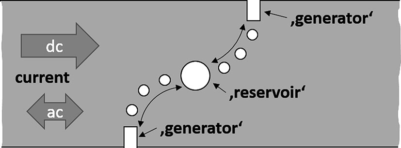
Sketch of different nano- and microstructure components for vortex manipulation in HTS films that might lead to novel fluxonic applications. Vortices and antivortices (vortices with inverted field component) can be generated by curls in the dc or microwave current caused by slits at opposite edges of a stripline, the ‘generators’ for vortex formation. Guidance, trapping, and annihilation are achieved by antidots of different size. Annihilation of vortices would be possible in the case of guidance of a vortex and an antivortex towards the same trapping site, the ‘reservoir’.
Generally, ratchets are formed from spatially asymmetric confining potentials. They can rectify oscillatory driving forces and generate directed motion. Ratchet scenarios were already considered by Feynman in his lecture notes in 1963 [75] and are related to earlier problems in thermodynamics studied by Smoluchowski in 1912 [76]. Ratchets represent a major component of particle transport in nanoscale systems, both in solid-state systems and in biology. Ratchets in biological systems (e.g., biomolecular motors) can be found in nature, including the kinesin and dynein proteins that provide transport functions within the cell [77]. Ratchets can be produced by biomolecular engineering, e.g., a molecular walker constructed from strands of DNA [78] and controlled motion of kinesin-driven microtubules along lithographically patterned tracks have been demonstrated recently [79]. Advances in nanofabrication made it feasible to develop and investigate ratchets formed from solid-state systems involving electronic devices or microfluidics. Such devices can be used (i) as analog systems for modeling biomolecular motors, (ii) to understand novel particle transport at the nanoscale or (iii) to develop new devices for application. One advantage of solid-state nanofabrication is the possibility to tailor the ratchet potential and to control driving parameters, temperature, or other process parameters. Implementations of ratchets in electronic devices have been demonstrated recently, e.g., the use of asymmetric structures of electrostatic gates above a 2D electron gas [80] and arrays of Josephson junctions with asymmetric critical currents [81].
Vortices in superconductors form an ideal system for exploring ratchet phenomena. The control of vortex dynamics via micro- or nanostructures allows for the tailoring of vortex-confining potentials. One approach for controlling and rectifying vortex motion in superconductors involves the use of arrays of antidots. Vortex ratchet effects obtained by various arrangements of antidots have recently been demonstrated for low-
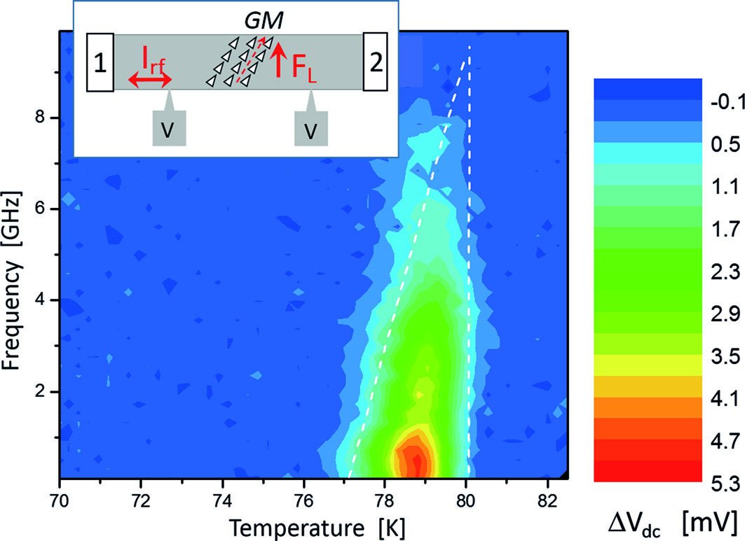
Demonstration of the ratchet effect in HTS microwave devices. Schematic drawing of a YBCO ratchet based on rows of triangularly shaped antidots (inset) and contour plot of the change of the dc voltage signal
Figure 15 shows an example of a HTS ratchet that also illustrates the potential use of ratchets in microwave applications. The design of the device (Figure 15a) is similar to the design used for the demonstration of guided vortex motion (see Figure 6), except for the fact, that asymmetric (here, triangular shaped) antidots are used. The tilting of the direction of antidot rows with respect to the Lorentz force allows for simultaneous measurements of a longitudinal and Hall signal in the case of guided vortex motion. In the case of the rectification of the vortex motion (ratchet effect) a microwave driving current would be transformed into a directional motion of vortices and, thus, a dc voltage at the Hall and longitudinal voltage pads. Figure 15b shows a contour plot of the dc voltage (only the longitudinal voltage is shown) obtained in a typical experiment. In order to improve the resolution of the measurement, a reference signal taken at low microwave power (
The experiment demonstrates that HTS vortex ratchets can operate, although in a restricted temperature regime close to
The principle of the vortex ratchet is one of the most interesting components for basic analysis and maybe also in the future for application of vortex manipulation in superconducting films and devices. Its operation has been demonstrated. They might be used as a converter (microwave-to-dc), filters, or as a component in more complex microwave devices that could offer interesting and novel properties.
5 Conclusions
Vortex matter in superconducting films and devices is not only an interesting topic for basic research but plays a substantial role in the applications of superconductivity in general. In most electronic applications, magnetic flux will penetrate the superconductor. Magnetic flux and flux motion affect the performance of superconducting devices. For instance, the reduction of the sensitivity in SQUIDs or the power-handling capability in microwave devices, or the increase of the error rate in logic devices is a consequence of the presence of flux and flux motion in these devices. Guidance and trapping of vortices can reduce or even prevent this effect.
Moreover, vortex manipulation is not only a useful tool to avoid degradation of superconducting device properties, it can also be used to analyze and understand novel and interesting physical properties and to develop new concepts for superconductor applications. Various concepts for vortex manipulation are sketched. The advantage of the use of micro- and nanopatterns (especially, antidots) for guiding and trapping of vortices is discussed and experimental evidence of vortex guidance and vortex trapping by various arrangements of antidots is given.
Thus, the vortex state of matter appears to be very important in applications of superconductivity and requires further investigation. A better understanding will clearly lead to an improvement of the performance of superconductor components, such as reduced noise, better power-handling capability, or improved reliability. Furthermore, it promises deeper insight into the basic physics of vortices and vortex matter, especially at high frequencies. The use of different experimental techniques in combination with micro- or even nanopatterning of high-
Acknowledgements
The author would like to acknowledge the experimental work of A. M. Castellanos, P. Selders, M. Pannetier, R. Wijngaarden, A. Pruymboom, P. Dymachevski, and P. Lahl.
This article is also available in: Wördenweber Superconductors at the Nanoscale. De Gruyter (2017), isbn 978-3-11-045620-2.
References
[1] Prozorov R, Kończykowski M, Tanatar MA, Thaler A, Bud’ko SL, Canfield PC, Mishra V, Hirschfeld PJ. Phys. Rev. X 4:041032, 2014.10.1103/PhysRevX.4.041032Suche in Google Scholar
[2] Pruymboom A, Kes PH, van der Drift E, Radelaar S, Appl. Phys. Lett. 52:662, 1988; Pruymboom A, Kes PH, van der Drift E, Radelaar S. Phys. Rev. Lett. 60:1430, 1988.Suche in Google Scholar
[3] Besseling R. Thesis, University of Leiden, 2001.Suche in Google Scholar
[4] Castellanos AM, Wordenweber R, Ockenfuss G, A. v.d. Hart, Keck K. Appl. Phys. Lett. 71:962, 1997.10.1063/1.119701Suche in Google Scholar
[5] Wordenweber R, Castellanos AM, Selders P. Physica C 332:27, 2000.10.1016/S0921-4534(99)00639-5Suche in Google Scholar
[6] Wordenweber R, Dymashevski P, Misko VR. Phys. Rev. B 69:184504, 2004.10.1103/PhysRevB.69.184504Suche in Google Scholar
[7] Laviano F, Ghigo G, Mezzetti E, Hollmann E, Wordenweber R. Control of the vortex flow in microchannel arrays produced in YBCO films by heavy-ion lithography, Physica C 19:844–847, 2010.10.1016/j.physc.2010.02.052Suche in Google Scholar
[8] Gonzalez MP, Hollmann E, Wordenweber R. J. Appl. Phys. 102:063904, 2007.10.1063/1.2781515Suche in Google Scholar
[9] Kokubo N. Phys. Rev. Lett. 88:247004, 2002.10.1103/PhysRevLett.88.247004Suche in Google Scholar
[10] Yu K, Heitmann TW, Song C, DeFeo MP, Plourde BLT, Hesselberth MBS, Kes PH. Phys. Rev. B 76:220507, 2007.10.1103/PhysRevB.76.220507Suche in Google Scholar
[11] Selders P, Wordenweber R. Appl. Phys. Lett. 76:3277, 2000.10.1063/1.126605Suche in Google Scholar
[12] Wordenweber R, Selders P. Physica C 366:135, 2002.10.1016/S0921-4534(01)00837-1Suche in Google Scholar
[13] Berdiyorov GR, Milošević MV, Peeters FM. ‘Qualitative modification of the pinning force due to vortex-cavity adherence in perforated superconducting films’, unpublished.Suche in Google Scholar
[14] Mkrtchyan GS, Shmidt VV. Sov. Phys. JETP 34:195, 1972.Suche in Google Scholar
[15] Buzdin AI, Feinberg D. Physica C 256:303, 1996.10.1016/0921-4534(95)00664-8Suche in Google Scholar
[16] Lahl P, Wordenweber R. Appl. Phys. Lett. 81:505, 2002.10.1063/1.1487902Suche in Google Scholar
[17] Bothner D, Gaber T, Kemmler M, Koelle D, Kleiner R. Appl. Phys. Lett. 98:102504, 2011.10.1063/1.3560480Suche in Google Scholar
[18] Bothner D, Clauss C, Koroknay E, Kemmler M, Gaber T, Jetter M, Scheffler M, Michler P, Dressel M, Koelle D, Kleiner R. Appl. Phys. Lett. 100:012601, 2012.10.1063/1.3673869Suche in Google Scholar
[19] Baert M, Metlusko VV, Jonckheere R, Moshchalkov VV, Bruynseraede Y. Phys. Rev. Lett. 74:3269, 1995.10.1103/PhysRevLett.74.3269Suche in Google Scholar
[20] Rosseel E, van Bael M, Baert M, Jonckheere R, Moshchalkov VV, Bruynserade Y. Phys. Rev. B 53:R2983, 1996.10.1103/PhysRevB.53.R2983Suche in Google Scholar
[21] Metlushko VV, Baert M, Jonckheere R, Moshchalkov VV, Bruynserade Y. Sol. St. Comm. 91:331, 1994.10.1016/0038-1098(94)90628-9Suche in Google Scholar
[22] Moshchalkov VV, Baert M, Rosseel E, Metlushko VV, van Bael MJ, Bruynserade Y. Physica C 282:379, 1997.10.1016/S0921-4534(97)00280-3Suche in Google Scholar
[23] Moshchalkov VV, Baert M, Metlushko VV, Rosseel E, van Bael MJ, Temst K, Bruynserade Y, Jonckheere R. Phy. Rev. B 57:3615, 1998.10.1103/PhysRevB.57.3615Suche in Google Scholar
[24] van Look L, Rosseel E, van Bael MJ, Temst K, Moshchalkov VV, Bruynseraede Y. Phys. Rev. B 60:R6998, 1999.10.1103/PhysRevB.60.R6998Suche in Google Scholar
[25] Lykov AN. Sol. St. Comm. 86:531, 1993.10.1016/0038-1098(93)90103-TSuche in Google Scholar
[26] Harada K, Kamimura O, Kasai H, Matsuda T, Tonomura A, Moshchalkov VV. Science 274:1167, 1996.10.1126/science.274.5290.1167Suche in Google Scholar PubMed
[27] Bezryadin A, Ovchinikov YN, Pannetier B, Phys. Rev. B 53:8553, 1996; Bezryadin A, Pannetier B. J. Low Temp. Phys. 102:73, 1996.Suche in Google Scholar
[28] Metlushko VV, Welp U, Crabtree GW, Zhao Zhang, Brueck SRJ, Watkins B, DeLong LE, Ilic B, Chung K, Hesketh PJ. Phys. Rev. B 59:603, 1999.10.1103/PhysRevB.59.603Suche in Google Scholar
[29] Metlushko VV, Welp U, Crabtree GW, Osgood R, Bader SD, DeLong LE, Zhao Zhang, Brueck SRJ, Ilic B, Chung K, Hesketh PJ. Phys. Rev. B 60:R12585, 1999.10.1103/PhysRevB.60.R12585Suche in Google Scholar
[30] Wordenweber R, Hollmann E, Schubert J, Kutzner R. and Ajay Kumar Ghosh, Appl.Phys. Lett. 94:202501, 2009.10.1063/1.3139077Suche in Google Scholar
[31] Nordborg H, Vinokur VM. Phys. Rev. B 62:12408, 2000.10.1103/PhysRevB.62.12408Suche in Google Scholar
[32] Bean CP, Livingston JD. Phys. Rev. Lett. 12:14, 1964.10.1103/PhysRevLett.12.14Suche in Google Scholar
[33] Surdeanu R, Wijngaarden RJ, Griessen R, Einfeld J, Wordenweber R. Europhys. Lett. 54:682, 2001.10.1209/epl/i2001-00369-6Suche in Google Scholar
[34] Moshchalkov VV, Baert M, Metlushko VV, Rosseel E, van Bael MJ, Temst K, Jonckheere R, Bruynserade Y. Phys. Rev. B 54:7385, 1996.10.1103/PhysRevB.54.7385Suche in Google Scholar PubMed
[35] Misko V, Savel’ev S, Nori F. Phys. Rev. Lett. 95:177007, 2005.10.1103/PhysRevLett.95.177007Suche in Google Scholar PubMed
[36] Kemmler. M, Gurlich C, Sterck A, Pohler H, Neuhaus M, Siegel M, Kleiner R, Koelle D. Phys. Rev. Lett. 97:147003, 2006.10.1103/PhysRevLett.97.147003Suche in Google Scholar
[37] Bothner D, Seidl R, Misko VR, Kleiner R, Koelle D, Kemmler M. Supercond. Sci. Technol. 27:065002, 2014.10.1088/0953-2048/27/6/065002Suche in Google Scholar
[38] Selders P, Castellanos AM, Vaupel M, Wordenweber R. Appl. Supercond. 5:269, 1998.10.1016/S0964-1807(97)00056-2Suche in Google Scholar
[39] Pannetier M, Wijngaarden RJ, Floan I, Rector J, Griessen R, Lahl P, Wordenweber R. Phys. Rev. B 67:212501, 2003.10.1103/PhysRevB.67.212501Suche in Google Scholar
[40] Lukashenko A, Ustinov AV, Zhuravel AP, Hollmann E, Wordenweber R. J. Appl. Phys. 100:023913, 2006.10.1063/1.2216819Suche in Google Scholar
[41] Hagen SJ, Lobb CJ, Greene RL, Forrester MG, Kang JH. Phys. Rev. B 41:11630, 1990.10.1103/PhysRevB.41.11630Suche in Google Scholar PubMed
[42] Hagen SJ, Smith AW, Rajeswari M, Peng JL, Li ZY, Greene RL, Mao SN, Xi XX, Bhattacharya S, Li Q, Lobb CJ. Phys. Rev. B 47:1064, 1993.10.1103/PhysRevB.47.1064Suche in Google Scholar
[43] Ao P. J. Phys. Condens. Matter 10:L677, 1998.10.1088/0953-8984/10/41/002Suche in Google Scholar
[44] Jensen HJ, Minnhagen P, Sonin E, Weber H. Europhys. Lett. 20:463, 1992.10.1209/0295-5075/20/5/014Suche in Google Scholar
[45] Ferrell RA. Phys.Rev. Lett. 68:2524, 1992.10.1103/PhysRevLett.68.2524Suche in Google Scholar PubMed
[46] van Otterlo A, Feigel’man M, Geshkenbein V, Blatter G. Phys. Rev. Lett. 75:3736, 1995.10.1103/PhysRevLett.75.3736Suche in Google Scholar
[47] Khomskii DI, Freimuth A. Phys. Rev. Lett. 75:1384, 1995.10.1103/PhysRevLett.75.1384Suche in Google Scholar
[48] Kopnin NB. Phys. Rev. B 54:9475, 1996.10.1103/PhysRevB.54.9475Suche in Google Scholar
[49] Kolacek J, Vasek P. Physica C 336:199, 2000.10.1016/S0921-4534(00)00286-0Suche in Google Scholar
[50] Wordenweber R, Sankarraj JSK, Dymashevski P, Hollmann E. Physica C 434:101, 2006.10.1016/j.physc.2005.11.014Suche in Google Scholar
[51] Larkin AI, Ovchinnikov YuN. Zh. Eksp. Teo. Fiz. 68:1915, 1975; Sov. Phys.-JETP 41:960, 1976.Suche in Google Scholar
[52] Skocpol WJ, Beasley MR, Tinkham M. J. Low. Temp. Phys. 16:145, 1974.10.1007/BF00655865Suche in Google Scholar
[53] Kadin AM, Smith LN, Skocpol WJ. J. Low Temp. Phys. 38:497, 1980.10.1007/BF00114339Suche in Google Scholar
[54] Musienko LE, Dmitrenko IM, und Volotskaya VG. Pis’ma Zh. Eksp. Teor. Fiz. 31:603, 1980; JETP Lett. 31:567, 1980.Suche in Google Scholar
[55] Klein W, Huebener RP, Gauss S, und Parisi J. J. Low. Temp. Phys. 61:413, 1985.10.1007/BF00683694Suche in Google Scholar
[56] Doettinger SG, Huebener RP, Gerdemann R, Kuhle A, Anders S, Trauble TG, Villegier JC. Phys.Rev. Lett. 73:1691, 1994; Physica C 235–240:3179, 1994.10.1016/0921-4534(94)91116-9Suche in Google Scholar
[57] Doettinger SG, Huebener RP, Kuhle A. Physica C 251:285, 1995.10.1016/0921-4534(95)00411-4Suche in Google Scholar
[58] Lahl P, Wordenweber R. Inst. Phys. Conf. Ser. 158:77, 1997.Suche in Google Scholar
[59] Grimaldi G, Leo A, Sabatino P, Carapella G, Nigro A, Pace S, Moshchalkov VV, Silhanek AV. Phys. Rev. B 92:024513, 2015.10.1103/PhysRevB.92.024513Suche in Google Scholar
[60] Wordenweber R, Kruger U, Schneider J, Kutzner R, Ockenfu G. s, Inst. of Phys. Conf. Ser. 148:619, 1995.Suche in Google Scholar
[61] Kuznetsov VI, Tulin VA. Sov. Phys. JETP 86:1364, 1998.10.1134/1.558535Suche in Google Scholar
[62] Weber A, Kramer L. J. Low Temp. Phys. 84:289, 1991.10.1007/BF00683522Suche in Google Scholar
[63] Schneider J, Kohlstedt H, Wordenweber R. Appl. Phys. Lett. 63:2426, 1993.10.1063/1.110496Suche in Google Scholar
[64] Sivakov AG, Glukhov AM, Omelyanchouk AN, Koval Y, Muller P, Ustinov AV. Phys. Rev. Lett. 91:267001, 2003.10.1103/PhysRevLett.91.267001Suche in Google Scholar
[65] Andronov A, Gordion I, Kurin V, Nefedov I, Shereshevsky I. Physica C 213:193, 1993.10.1016/0921-4534(93)90777-NSuche in Google Scholar
[66] Zeldov E, Larkin AI, Geshkenbein VB, Konczykowski M, Majer D, Khaykovich B, Vinokur VM, Shtrikman H. Phys. Rev. Lett. 73:1428, 1994.10.1103/PhysRevLett.73.1428Suche in Google Scholar PubMed
[67] Gross R, Mayer B, Physica C 180:235, 1991; Kawasaki M, Chaudhari P, Gupta A, Phys. Rev. Lett. 68:1065, 1992; Marx A, Gross R, Appl. Phys. Lett. 70:120, 1997; Miklich AH, Clarke J, Colclough MS, Char K. Appl. Phys. Lett. 60:1899, 1992.Suche in Google Scholar
[68] Forgacs RL, Warwick AF, Rev. Sci. Instrum. 38:214, 1967; Foglietti V, Gallagher WJ, Ketchen MB, Kleinsasser AW, Koch RH, Raider SI, and Sandstrom RL, Appl. Phys. Lett. 49:1393, 1986; Koch RH, Clarke J, Goubau WM, Martinis JM, Pegrum CM, and van Harlingen DJ, J. Low Temp. Phys. 51:207, 1983; Koch RH, Robertazzi RP, Andrek SA, and Gallagher WJ, Appl. Phys. Lett. 60:507, 1992; Miklich AH, Koelle D, Dantsker E, Nemeth DT, Kingston JJ, Kromann RF, Clarke J, IEEE Trans. Appl. Supercond. 3:2434, 1993; Muck M, Heiden C, Clarke J. J. Appl. Phys. 75:4588, 1994.Suche in Google Scholar
[69] Dutta P, Dimon P, Horn PM. Phys. Rev. Lett. 60:646, 1979; Dutta P, Horn PM. Rev. Mod. Phys. 53:497, 1981.Suche in Google Scholar
[70] Golod T, Iovan A, Krasnov VM. Nat. Comm. 6:8628, 2015.10.1038/ncomms9628Suche in Google Scholar PubMed PubMed Central
[71] Vendik IB, Vendik OG, Kaparkov DI. Superconductor Microwave Technology, Part II: Superconducting Microwave Circuits. Report No 24, Kollberg E (ed), Chalmers University of Technology, 1996.Suche in Google Scholar
[72] Wordenweber R. High-Tc films: From natural defects to nanostructure engineering of vortex matter. In: Moshchalkov V, Wordenweber R, Lang W (eds). Nanoscience and Engineering in Superconductivity. Series: NanoScience and Technology, Springer, p. 25–80, 2010.10.1007/978-3-642-15137-8_2Suche in Google Scholar
[73] Baziljevich M, Johansen TH, Bratsberg H, Shen Y, Vase P. Appl. Phys. Lett. 69:3590, 1996.10.1063/1.117216Suche in Google Scholar
[74] Yurchenko VV, Wordenweber R, Galperin YuM, Shantsev DV, Vestgarden JI, Johansen TH. Physica C 437–438:357, 2006.10.1016/j.physc.2005.12.075Suche in Google Scholar
[75] Feynman RP, Leighton RB, Sands M, The Feynman Lectures on Physics, vol. I. Addison-Wesley, Reading, MA, 1963.Suche in Google Scholar
[76] Smoluchowski M. Phys. Z. 13:1069, 1912.Suche in Google Scholar
[77] Kay E, Leigh D, Zerbetto F. Angew. Chem. Int. 46:72, 2007.10.1002/anie.200504313Suche in Google Scholar
[78] Omabegho T, Sha R, Seeman NC. Science 324:67, 2009.10.1126/science.1170336Suche in Google Scholar
[79] Hiratsuka Y, Tada T, Oiwa K, Kanayama T, Uyeda T. Biophys. J. 81:1555, 2001.10.1016/S0006-3495(01)75809-2Suche in Google Scholar
[80] Linke H, Humphrey TE, Lofgren A, Sushkov AO, Newbury R, Taylor RP, Omling P. Science 286:2314, 1999.10.1126/science.286.5448.2314Suche in Google Scholar PubMed
[81] Shalom DE, Pastoriza H. Phys. Rev. Lett. 94:177001, 2005.10.1103/PhysRevLett.94.177001Suche in Google Scholar PubMed
[82] Zhu BY, Marchesoni F, Moshchalkov VV, Nori F. Phys. Rev. B 68:014514, 2003.10.1103/PhysRevB.68.014514Suche in Google Scholar
[83] Van de Vondel J, de Souza Silva CC, Zhu BY, Morelle M, Moshchalkov VV. Phys. Rev. Lett. 94:057003, 2005.10.1103/PhysRevLett.94.057003Suche in Google Scholar PubMed
[84] de Souza Silva CC, Van de Vondel J, Zhu BY, Morelle M, Moshchalkov VV. Phys. Rev. B 73:014507, 2006.10.1103/PhysRevB.73.014507Suche in Google Scholar
[85] de Souza Silva CC, Van de Vondel J, Morelle M, Moshchalkov VV. Nature 440:651, 2006.10.1038/nature04595Suche in Google Scholar PubMed
© 2017 Wördenweber, published by De Gruyter
This work is licensed under the Creative Commons Attribution-NonCommercial-NoDerivatives 4.0 License.
Artikel in diesem Heft
- Improved epoxy thermosets by the use of poly(ethyleneimine) derivatives
- NanoSQUIDs: Basics & recent advances
- Computational chemistry applied to vibrational spectroscopy: A tool for characterization of nucleic acid bases and some of their 5-substituted derivatives
- Polymers application in proton exchange membranes for fuel cells (PEMFCs)
- Engineering of superconductors and superconducting devices using artificial pinning sites
- Educational benefits of green chemistry
- Spectroscopic properties of polymer composites