Resistive switching characteristics and mechanisms in silicon oxide memory devices
-
Yao-Feng Chang
 ,
Burt Fowler
,
Burt Fowler

Abstract
Intrinsic unipolar SiOx-based resistance random access memories (ReRAM) characterization, switching mechanisms, and applications have been investigated. Device structures, material compositions, and electrical characteristics are identified that enable ReRAM cells with high ON/OFF ratio, low static power consumption, low switching power, and high readout-margin using complementary metal-oxide semiconductor transistor (CMOS)–compatible SiOx-based materials. These ideas are combined with the use of horizontal and vertical device structure designs, composition optimization, electrical control, and external factors to help understand resistive switching (RS) mechanisms. Measured temperature effects, pulse response, and carrier transport behaviors lead to compact models of RS mechanisms and energy band diagrams in order to aid the development of computer-aided design for ultralarge-v scale integration. This chapter presents a comprehensive investigation of SiOx-based RS characteristics and mechanisms for the post-CMOS device era.
1 Introduction
Floating gate (FG) memory has been the primary structure used for nonvolatile memory (NVM) devices since its invention in 1967 by D. Kahng and S. M. Sze and has been widely employed in the portable electronic products such as mobile phones, digital cameras, notebook computers, mp3 players, and USB flash drives. The operating principle of conventional NVM is based on the use of polycrystalline silicon as an FG to store charges injected from a channel [1]. However, as device size continues to shrink, the typical flash memory device will continue to suffer from degraded retention and endurance [2]. In order to solve these problems, researchers have presented two main methods to improve memory devices with different storage technologies. The first is to change the storage layer without changing the device structure, and the second is to propose novel structures. In order to change the storage layer, either silicon nitride [3] or discrete nanocrystals [4, 5] have been employed as storage cells. However, making changes to the storage layer cannot fully resolve issues related to scaling down device size and increasing program/erase speed. Therefore, researchers have considered new storage layers and novel structures in NVM devices to replace the conventional FG device. New NVM devices must exhibit faster program/erase speeds and higher endurance. As for device size scale-down requirements [6–11], new devices should be compatible with a cross-point structure. Over the past decade, numerous potential memory structures have been proposed, with some being transferred into production lines, such as phase change memory (PCM), magnetic random access memory (MRAM), and ferroelectric random access memory (FeRAM). More recently, resistance random access memories (ReRAMs) have gained significant research interest as an alternative for next-generation NVM due to their high density, low cost, low power consumption, fast switching speed, and simple cell structure [12–22]. In addition, ReRAM technology can achieve program/erase speeds as high as static random access memory (SRAM) and densities as large as dynamic random access memory (DRAM), while retaining the non-volatile properties of flash memory; therefore, ReRAMs demonstrate very good potential for replacing NAND flash, a type of FG memory, to become the next-generation NVM.
The structure of ReRAM devices consists of sandwiched metal/insulator/metal (MIM) layers. By applying voltage or current, the resistance of the device can be changed, thereby providing data storage capability. ReRAM first originated from Hickmott in the 1960s; he discovered that the resistance of AlOx could be modified after applying a voltage or current. The logic state “0” or “1” is defined by different resistance values and can be read by applying a low voltage to measure the resistance state. In recent years, resistive switching characteristics of a large variety of materials have been reported, including binary metal oxides such as NiO, CuO, and HfOx. ReRAM devices exhibit good nonvolatile characteristics, and the stored data are retained until the next data are written. Characteristics such as low operating voltage, fast program/erase speed, and good scale-down capability make ReRAM a suitable candidate for the next-generation NVM. Hence, ReRAM is gaining significant interest in academia and industry for its high practicality and potential for commercial use.
In this chapter, SiOx-based ReRAM characteristics, mechanisms, and potential applications are reviewed [23–49]. Deep insights into resistive switching characteris-tics are provided. Possible resistive switching mechanisms are investigated, including an example of RS model based on proton exchange reactions that describe device transitions between high-resistance state (HRS) and low-resistance state (LRS). These studies regarding novel SiOx-based ReRAM and related physical mechanisms represent a significant contribution to the development of next-generation NVM.
2 Results and discussion
2.1 Device structure, materials, and electrical control for SiOx-based ReRAM
2.1.1 Post-deposition anneal and polarity effects
Recent reports by Yao et al. on SiOx-based resistive switching in vacuum indicate that this traditionally passive material can be converted to an active memory material by external electrical activation [35, 36]. Although many resistive switching mechanisms have been reported for various materials 37, 38, the exact switching mechanisms in SiOx-based materials have yet to be identified and may be different than traditional materials. Therefore, characterizing the polarity dependence of device switching is a top priority for the unipolar, SiOx-based resistive switching memory. Specifically, analyzing and understanding device RESET switching parameters will help develop a resistive switching model. In Figure 1, SiOx-based resistive switching memory is realized by fabricating a tantalum nitride (TaN)/SiO2/ heavily doped n-type (n++) Si-substrate structure. Device switching characteristics and stability were investigated with and without a postdeposition anneal (PDA). The polarity dependence of switching characteristics suggests that the switching region is located at the cathode side, potentially due to the asymmetrical thermal-dissipation structure of the TaN/SiO2/n++ Si device. Also, data retention tests in the HRS and LRS for over 104 seconds confirm the nonvolatile nature of the device. Testing several different device structures enables the development of a possible resistive switching model to aid characterizing SiOx-based devices for use in future ReRAM applications.
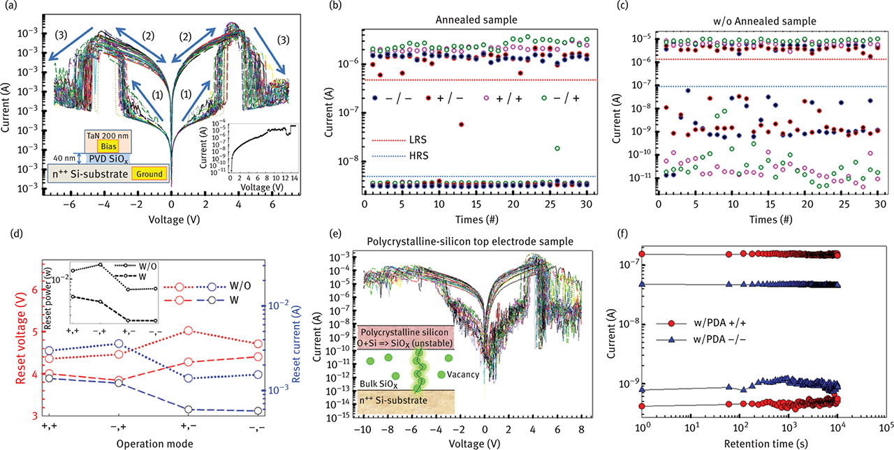
Thirty cycles of resistive switching behavior in samples with PDA. Arrows indicate voltage sweep directions. Left and right insets show a schematic representation of the TaN/SiO2/n++ Si-substrate structure and an I–V plot of electroforming data, respectively. (b) and (c) Polarity dependence of LRS and HRS distributions across 30 cycles for samples (b) with and (c) without 5 min 500°C PDA in O2. In (b), −/− means negative SET/negative RESET. (d) Polarity dependence of RESET voltage, RESET current, and RESET power (inset) for samples with and without PDA. (e) Polycrystalline-silicon top electrode device switching characteristics and O− ion reaction with Si in polycrystalline-silicon electrode to form SiOx (inset). (f) Retention test at room temperature for samples without PDA in positive and negative polarity conditions.
2.1.2 Horizontal and vertical device structure designs, composition optimization (SiOx, x < 2), and electrical control characterizations
In Figure 2, the oxygen content effect in SiOx-based ReRAM has been investigated by controlling the O2 flow rate during reactive sputtering of Si in an O2 ambient. It has been found that device yield, switching characteristics, and stability are all improved for device layers with near-stoichiometric oxygen content (i.e.,x ~ 2). The effects of SiOx thickness, device area, and multilevel operation by controlling set compliance current and reset voltage suggest that the switching region is located at the interface and is localized rather than occurring uniformly throughout the bulk SiOx layer. Also, the current transport behaviors in the HRS and LRS have been studied. A general current flow model for unipolar SiOx-based resistive switching memory has been proposed, which provides a simple physical concept to describe RS behavior and provides additional insights into optimization of ReRAM devices.
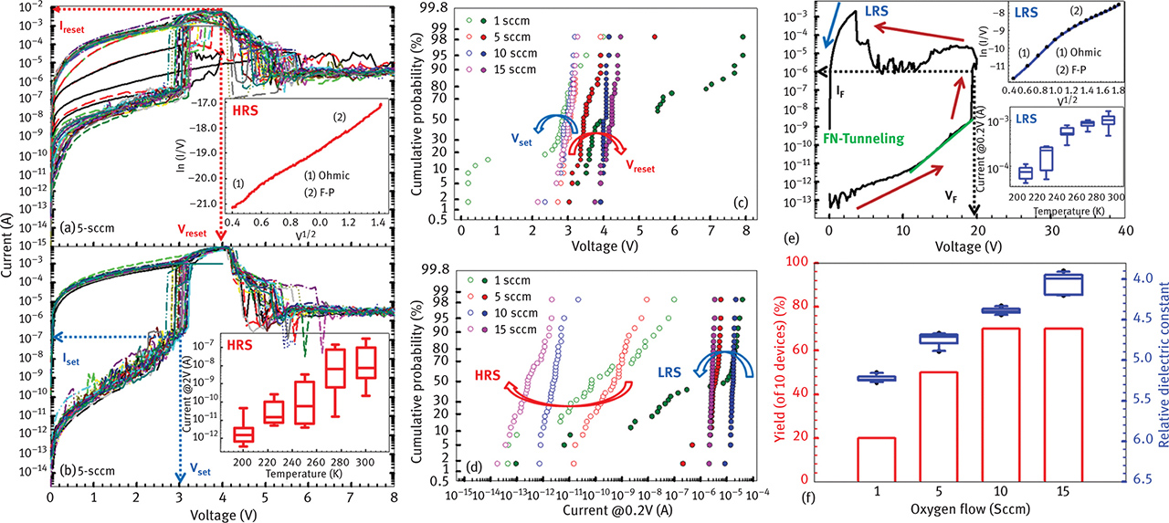
Thirty cycles of unipolar switching behaviors of samples deposited using reactive sputtering with (a) 5 sccm of O2 and (b) 10 sccm of O2 with compliance current of 1 mA applied during the set process. Top and bottom insets show a plot of ln(I/V) versus V1/2 and a plot of current versus temperature in HRS. Distribution of (c) VSET/VRESET and (d) HRS/LRS current as a function of O2 flow. (e) Electroforming I–V response of 15-sccm (Standard cubic centimeter per minute) sample. Right top and right bottom insets show a plot of ln(I/V) versus V1/2 and a plot of current versus temperature in LRS. Arrows indicate voltage sweep directions. (f) Device yield and relative dielectric constant as function of oxygen flow rate in SiOx deposition process.
2.1.3 Ambient effects and bimodal failure phenomenon
In addition to excellent insulating properties, SiOx-based materials have recently demonstrated resistive switching phenomena in both vacuum and atmosphere ambients. The devices exhibit unique unipolar operating characteristics where turn-off voltage is the same as or larger in magnitude than the turn-on voltage. In addition, resistive switching occurs only in nonoxidizing ambients. Although several potential resistive switching mechanisms have been reported for SiOx-based devices, the exact switching mechanisms are still not well understood. In Figure 3, the sensitivity to oxygen in SiOx-based ReRAM has been investigated by controlling the ambient gas pressure and monitoring resistive switching characteristics. Operating stability measurements in vacuum, nitrogen, and oxygen–nitrogen ambients show that SiOx-based ReRAM is sensitive to oxygen partial pressure, where resistive switching is temporarily disabled for O2 partial pressures above 2 Torr. Interestingly, a subsequent vacuum recovery process restores normal functionality. The statistical distribution of electrical parameters in the oxygen-induced failures can be described using bimodal Monte Carlo simulations and additional failure analysis. Potential solutions for a unique resistive-switching-type oxygen sensor and packaging methods for SiOx-based ReRAM are described for the development of clear design criteria for future applications.
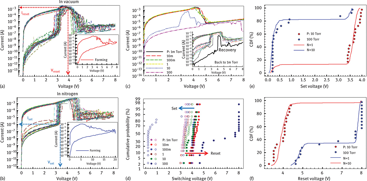
The resistive switching behaviors and forming processes (insets) in (a) vacuum and (b) N2 ambients. (c) Average current for 20 SET/RESET cycles for different pressures of 20% O2–N2 and the device recovery process in vacuum (inset). (d) Cumulative probability of switching voltage as function of 20% O2–N2 pressure. Initiation of resistive switching failures above 10 Torr of 20% O2–N2 mixture showing the cumulative distribution function using bi-modal Monte Carlo simulation fitting for (e) SET and (f) RESET voltage.
2.1.4 Edge and bulk device structures, an unusual backward-scan effect, and circuit-level simulation
Several “extrinsic” SiOx-based resistive switching behaviors have been reported, which may result from doping-induced filament formation during the fabrication process or highly diffusive, stacked electrode structures, but the “intrinsic” switching mechanisms are still not well understood. ReRAM devices using SiOx as the active switching medium have unusual electrical characteristics where resistive switching occurs only in nonoxidizing ambients and a unique unipolar operation where RESET voltage is typically larger in magnitude than SET voltage [33]. Current increases with temperature and is fairly independent of device area and SiOx thickness, indicating that switching occurs in a localized region along a conductive filament. Device structures typically incorporate an etched sidewall to increase electroforming yield. In previous reports, the unique unipolar operation of SiOx-based ReRAM has been investigated by controlling the external resistance using a series transistor (1T) and monitoring resistive switching characteristics. A nonedge SiOx device demonstrates that resistive switching can occur in bulk SiOx materials and provides additional fabrication flexibility. Thermal anneal of bulk devices in reducing ambient improves device performance by hydrogen incorporation. An unusual backward-scan effect, where the device state is determined by the duration of the reverse sweep, is examined by DC and AC pulse measurements to quantify the requirements for programming duration during the RESET process (Figure 4). The switching behavior of the backward-scan effect is incorporated into Verilog-A simulations to characterize integration strategies for future circuit-level applications.
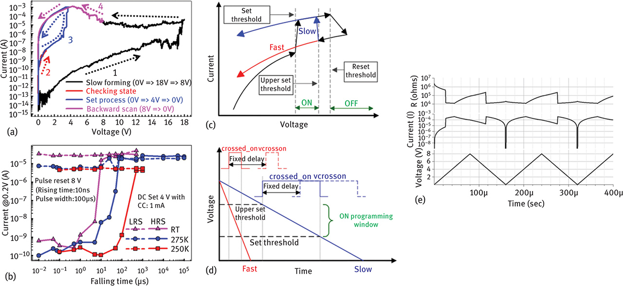
The backward-scan effect during a DC sweep: (1) Forming voltage sweep with slow rate (1,000 points in sweep range); (2) check of device state using a DC sweep from 0 V to 1 V; (3) SET process using a 4 V forward/reverse DC sweep with 1 mA compliance current limit; and (4) backward-scan effect in the SiOx device. (b) The backward-scan effect using AC pulses with controlled falling times versus temperature. The fast (red) and slow (blue) backward voltage sweeps are plotted in (c) I–V and (d) V–t form. In (d), the crossed_on and vcrosson signals linked to the time axis are used to determine whether the device will switch from the OFF to ON state. (e) Resistance (R), current (I), and voltage (V) simulation results demonstrating that the device switches from OFF to ON state during a slow backward voltage sweep.
2.1.5 Integrated one diode–one resistor (1D–1R) nanopillar architecture
By considering the static power consumption and sneak-path issues in large-scale crossbar array designs, a Schottky diode is not suitable for portable electronics due to its high reverse-bias leakage current and relatively low reverse-bias breakdown voltage as compared to a Si-based PN-diode or transistor. For example, the reverse leakage current of Schottky diodes can increase dramatically with temperature to the point of a thermal-runaway situation, potentially resulting in instability issues and readout failures. In Figure 5, a Si diode (1D) with low reverse-bias current is integrated with a SiOx-based memory element (1R) using nanosphere lithography (NS lithography, or NSL) and deep-Si-etching (DSE) to pattern a P++/N+/N++ epitaxial Si wafer. The self-aligned process forms a high-density, large-scale nanopillar (NP) array architecture. Compared with conventional photolithography or direct-writing methods (e.g., electron beam lithography or focused ion beam milling), NSL is demonstrated as a low-cost (maskless), high-throughput alternative technique to pattern large areas. The nanostructures fabricated using NSL can be well controlled in shape, size, and interpillar spacing through direct assembly of polymer nano-spheres on the wafer scale. Performance of 1R and 1D–1R structures is characterized and shows that the integrated nanopillar 1D–1R configuration offers low static power for suppression of sneak-path issues. The work reported here provides an efficient fabrication process and low reverse-bias current in a SiOx-based 1D–1R configuration for potential use in future ultra-large-scale NVM applications.
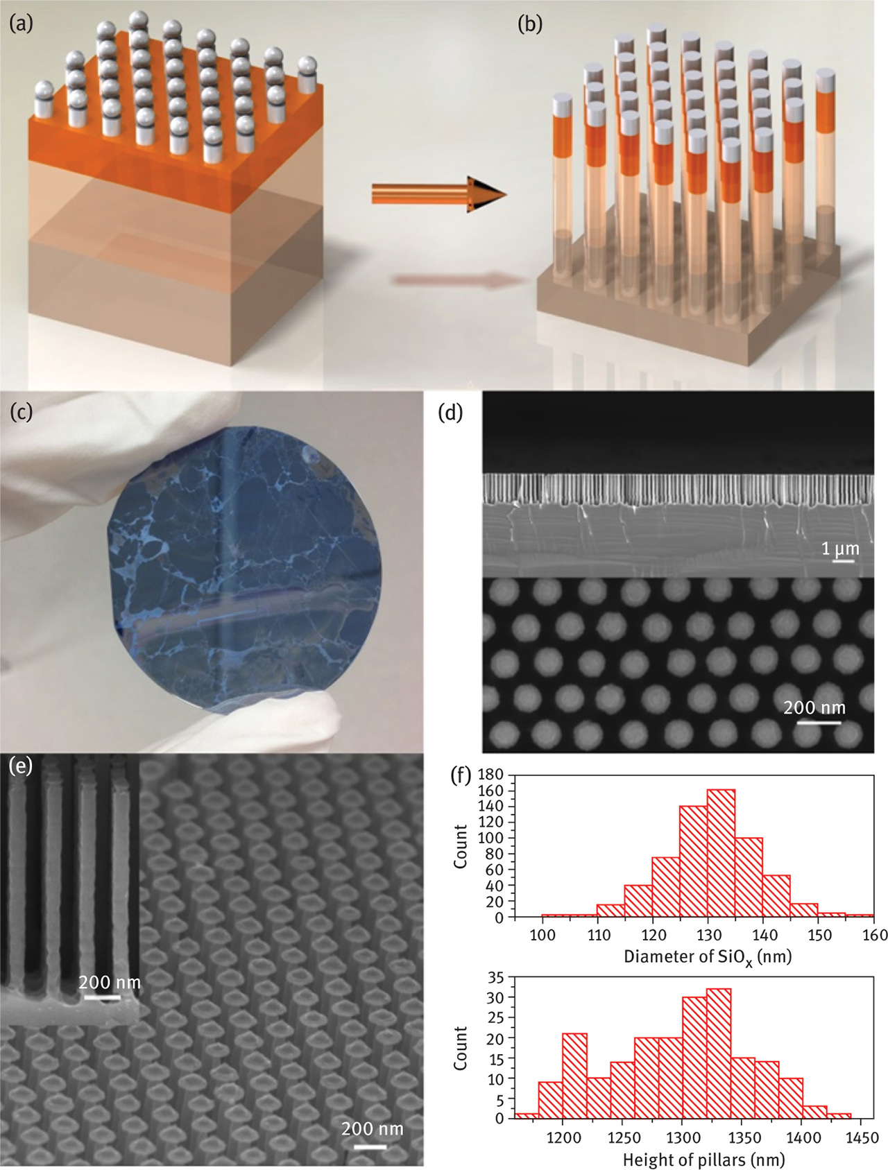
1D–1R fabrication process using DSE and device electrical characteristics: (a) Transfer of NSL pattern to SiOx hard-mask deposited on epitaxial P++/N+/N++ Si wafer. (b) DSE process in Bosch mode to form a self-aligned 1D–1R NP architecture. (c) Wafer scale and (d) and (e) SEM images of 1D–1R NPs. (f) Statistical distribution of nanopillar diameter and height.
2.2 Modeling of SiOx-based resistive switching mechanisms
2.2.1 Oxide stoichiometry effects on reversible switching and program window optimization
The achievements for intrinsic unipolar SiOx-based ReRAM include (1) high device yield, forming-free operation, reduced operating voltage, and excellent stability; (2) pulsed programing in the 50-ns regime for integrated 1D–1R cross-point arrays and sub-μA operating current in high-density 1D–1R architectures. However, characterization and modeling of current transport behaviors, defect transformations, energy band diagrams, and self-compliant mechanisms are not well understood. We analyze the effects of device structure, electrode material, SiOx thickness, and device area on electrical characteristics and confirm that RS occurs in a localized region along a conductive filament (CF), as shown in Figure 6. A physical model consistent with the observed RSI –V response is proposed. Several studies have used transmission electron microscopy to document the presence of Si nanocrystals within the CF, but it is not yet clear whether RS is the result of an overall increase in nanocrystal size or whether switching occurs in “GAP” regions in between nanocrystals. Most models of ReRAM switching involve the drift or diffusion of O2− ions (or oxygen vacancy defects), but these models cannot explain the unipolarI –V response or the ambient effects on RS observed in the SiOx device. Our RS model differs from most conventional models by considering that the defects responsible for RS may remain localized within the switching region so that RS occurs when a collection of defects are driven between conductive and nonconductive forms. Based on the reported electrical and structural properties of known SiOx defects, we further describe how proton exchange reactions can dramatically alter the conductivity of specific defects, leading to a model where the LRS has a large concentration of conductive defects within the switching region, and, conversely, when the device is programed to the HRS, most of the defects are converted to their nonconductive form. The electrically conductive hydrogen bridge (Si–H–Si) is viewed as the most likely defect responsible for the LRS. Electrochemical reactions that form the nonconductive (SiH)2 defect are discussed as potential mechanisms that enable localized switching without incorporating ion diffusion or drift mechanisms into the model. Our experimental results and RS model provide insights into device electrical characteristics and charge transport and may help identify localized, defect-driven switching mechanisms in SiOx-based ReRAM devices. Although the models described herein provide reasonable, accurate descriptions of RS in SiOx materials, it must be noted that direct evidence for the defects used in the models is likely to be very difficult, if not impossible, to obtain. Until direct evidence is found, the models represent a reasonable working hypothesis regarding RS mechanisms in SiOx materials.
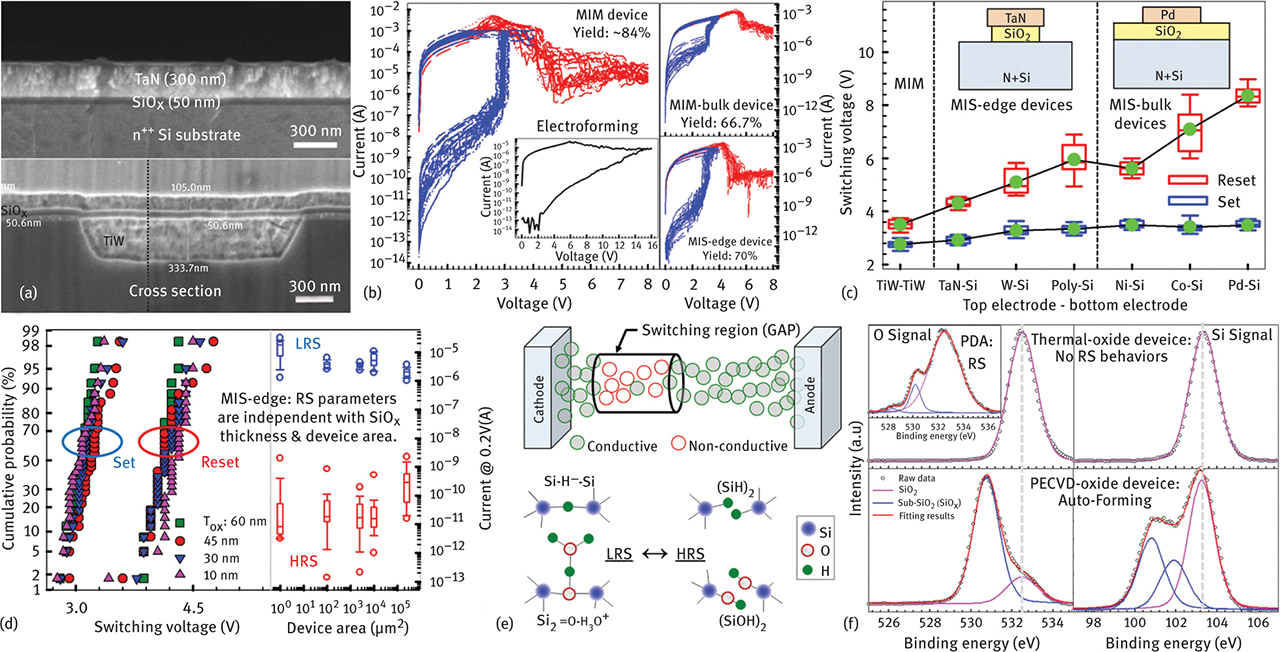
SEM images of TaN/SiOx/n++Si (MIS) structure in upper panel and TiW/SiOx/TiW (MIM) structure in lower panel. The MIM image is a composite (dashed line) showing the two ends of a single, 20-μm-wide, planarized TiW electrode. (b) Thirty cycles of unipolar switching I–V plots for MIM (electroforming process shown in the inset), MIS-bulk, and MIS-edge devices with corresponding yield labeled. (c) Effects of electrode material on SET and RESET switching voltages in MIM, MIS-edge, and MIS-bulk devices. The inset shows schematic of device structures of Mis-bulk and Mis-edge devices mean and represent in Fig.6 (c). (d) RS parameter dependence on SiOx thickness and device area in MIS-edge devices. (e) Physical representation of conductive filament with switching region (GAP) containing a mixture of conducting and nonconducting defect complexes. (b) Hypothesized defect complex in LRS (left) and HRS (right) representing potential electrochemical reaction products involved in switching, where the transfer of a single proton between two defects is responsible for RS. (f) O-1s and Si-2p XPS spectra and fitting results for low-pressure chemical vapor deposition thermal oxide, sputtered oxide with postdeposition anneal (PDA) treatment, and plasma-enhanced chemical vapor deposition oxide.
2.2.2 Thermal effects on charge transport and potential for multilevel programing
ReRAM devices can potentially be scaled to smaller sizes than NAND flash memory and are compatible with three-dimensional (3D) architectures, making ReRAM very attractive for future high-density production. Another way to improve storage density is through multilevel data storage where the memory element is capable of storing more than a single bit of information. For example, a cell that stores four states will yield two bits of information per cell. Therefore, a multilevel cell provides higher bit/cm2 density with lower cost and more economical manufacturing. Multistate storage is achieved in ReRAM by controlling the electrical programing conditions and requires that multiple resistance states have low programing variance so that each state is distinguishable from the others. Many RS mechanisms related to multilevel operation have been reported for various material systems and have successfully been incorporated into device operating models. One multilevel programing method that has been explored is using a compliance current limit (CCL) during the SET process [46], where an increase in CCL induces a more-robust, lower-resistance conductive filament and smaller CCL values are used to program a range of higher resistances. A second programing method is used to achieve higher resistance values by controlling the RESET voltage magnitude [46], where LRS/HRS current ratios as high as 108 can potentially be achieved.
To understand the RS mechanism, temperature dependence of device current provides additional information related to charge transport characteristics, such as electron energy barriers, average hopping distance, and the relative permittivity of the switching medium. We propose that the distinctive unipolar properties may result from proton exchange reactions during switching events that cause defect transformations between conductive and nonconductive forms (see Figure 6e). Here, specific defect energy levels are correlated to the switching transitions in theI – V response and the current overshoot phenomenon observed in the LRS [46], leading to energy band diagrams that further illustrate the switching transitions (Figure 7). The presented experimental results and physical switching model provide possible explanations for the distinctive unipolar operating characteristics of intrinsic SiOx-based resistive switching memory.
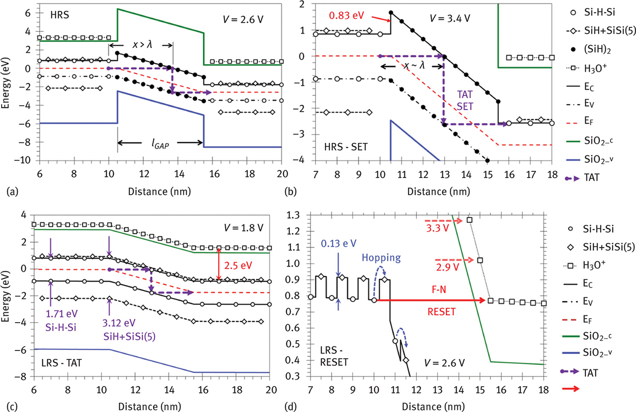
Energy band diagrams plotting electron potential energy versus distance along the conductive filament in the HRS. (a) Switching region with length lGAP = 6 nm filled with (SiH)2 defects for device biased to 2.6 V. (b) Energy barrier of 0.83 eV to electron transport from Si–H–Si defects into (SiH)2 defects and trap-assisted tunneling (TAT) to induce the SET transition at 3.4 V. Tunneling distance x and characteristic tunneling length λ are labeled in both plots to demonstrate the dependence of x on device bias. (c) Energy band diagram plotting electron potential energy versus distance along the conductive filament in the LRS. Switching region is filled with Si–H–Si, SiH + SiSi(5), and H3O+ defects showing available TAT pathway at 1.8 V bias. The effective bandgaps of the Si–H–Si and SiH + SiSi(5) defects and the 2.5 eV separation between Si–H–Si and H3O+ are labeled. (d) Energy barrier of 0.13 eV to electron hopping from Si–H–Si to SiH + SiSi(5), and F–N tunneling into H3O+ defects to induce the RESET transition at 2.6 V. Increasing bias above 2.6 V allows electron injection into neighboring H3O+ defects at 2.9 V and 3.3 V (dashed horizontal arrows), thus forming a conductance gap in the HRS.
3 Conclusion
In summary, we have elucidated device characteristics and defect-related resistive switching mechanisms in intrinsic unipolar SiOx-based ReRAM. This research investigates SiOx materials explicitly for use in next-generation nonvolatile memory applications and aims to advance memory device performance through novel device structures and better fabrication techniques.
Acknowledgment
This article is also available in: Liou (et al.), Nano Devices and Sensors. De Gruyter (2016), isbn 978-1-5015-1050.
References
[1] D. Kahng, S. M. Sze, Bell Syst. Tech, J. 46, 1288 (1967). (DOI: 10.1109/T-ED.1976.18468)Suche in Google Scholar
[2] J. De Blauwe, IEEE Trans. Nanotechnol. 1, 72 (2002). (DOI: 10.1109/TNANO.2002.1005428)Suche in Google Scholar
[3] H. E. Maes, G. Groeseneken, H. Lebon, J. Witters, Microelectronics Journal20, 9 (1989). (DOI: 10.1016/0026-2692(89)90122-5)Suche in Google Scholar
[4] S. Tiwari, F. Rana, K. Chan, H. Hanafi, C. Wei, D. Buchanan, Tech. Dig.– Int. Electron Devices Meet. 521 (1995). (DOI: 10.1109/IEDM.1995.499252)Suche in Google Scholar
[5] L. W. Feng, C. Y. Chang, T. C. Chang, C. H. Tu, P. S. Wang, Y. F. Chang, M. C. Chen, H. C. Huang, Appl. Phys. Lett. 95, 262110 (2009). (DOI: 10.1063/1.3279131)Suche in Google Scholar
[6] L. Ji, M. D. McDaniel, L. Tao, X. Li, A. B. Posadas, Y. F. Chang, A. Demkov, J. G. Ekerdt, D. Akin-wande, R. S. Ruoff, J. C. Lee, E. T. Yu, Tech. Dig.– Int. Electron Devices Meet. 8.6.1–8.6.3 (2014). (DOI: 10.1109/IEDM.2014.7047013)Suche in Google Scholar
[7] F. Xue, A. Jiang, Y. T. Chen, Y. Wang, F. Zhou, Y. F. Chang, J. C. Lee IEEE Transactions on Electron Devices61, 2332 (2014). (DOI: 10.1109/TED.2014.2320946)Suche in Google Scholar
[8] F. Zhou, F. Xue, Y. F. Chang, J. C. Lee, Device Research Conference (DRC), 2014 72nd Annual 207 (2014). (DOI: 10.1109/DRC.2014.6872370)Suche in Google Scholar
[9] F. Xue, A. Jiang, Y. T. Chen, Y. Wang, F. Zhou, Y. F. Chang, J. Lee, Tech. Dig.– Int. Electron Devices Meet. 27.5.1–27.5.4 (2012). (DOI: 10.1109/IEDM.2012.6479116)Suche in Google Scholar
[10] Y. Wang, Y. T. Chen, F. Xue, F. Zhou, Y. F. Chang, J. C. Lee, ECS Transactions50, 151 (2013). (DOI: 10.1149/05004.0151ecst)Suche in Google Scholar
[11] C. C Cheng, C. H. Chien, G. L. Luo, J. C. Liu, Y. C. Chen, Y. F. Chang, S. Y. Wang, C. C. Kei, C. N. Hsiao, C. Y. Chang, J. Vac. Sci. Technol. B27, 130 (2009). (DOI: 10.1116/1.3058724)Suche in Google Scholar
[12] Y. F. Chang, L. W. Feng, C. W. Huang, G. Y. Wu, C. H. Chang, J. J. Wu, S. Y. Wang, T. C. Chang, C. Y. Chang, 2011 IEEE 4th International Nanoelectronics Conference 1, (2011). (DOI: 10.1109/INEC.2011.5991628)Suche in Google Scholar
[13] Y. F. Chang, Y. T. Tsai, G. W. Chang, Y. E. Syu, Y. H. Tai, T. C. Chang. ECS J. Solid State Sci. Technol. 1, Q91 (2012). (DOI: 10.1149/2.003205jss)Suche in Google Scholar
[14] Y. F. Chang, T. C. Chang, C. Y. Chang. J. Appl. Phys. 110, 053703 (2011). (DOI: 10.1063/1.3630119)Suche in Google Scholar
[15] Y. F. Chang, L. W. Feng, T. C. Chang. Mater. Chem. Phys. 131, 262 (2011). (DOI: 10.1016/j.matchemphys.2011.09.037)Suche in Google Scholar
[16] Y. F. Chang, Y. T. Tsai, Y. E. Syu, T. C. Chang. ECS J. Solid State Sci. Technol. 1, Q57 (2012). (DOI: 10.1149/2.020203jss)Suche in Google Scholar
[17] L. W. Feng, Y. F. Chang, C. Y. Chang, T. C. Chang, S. Y. Wang, P. W. Chiang, C. C. Lin, S. C. Chen, S. C. Chen. Thin Solid Films519, 1536 (2010). (DOI: 10.1016/j.tsf.2010.08.165)Suche in Google Scholar
[18] L. W. Feng, C. Y. Chang, Y. F. Chang, T. C. Chang, S. Y. Wang, S. C. Chen, C. C. Lin, S. C. Chen, P. W. Chiang. Appl. Phys. Lett. 96, 222108 (2010). (DOI: 10.1063/1.3428777)Suche in Google Scholar
[19] K. C. Chang, T. C. Chang, T. M. Tsai, R. Zhang, Y. C. Hung, Y. E. Syu, Y. F. Chang, M. C. Chen, T. J. Chu, H. L. Chen, C. H. Pan, C. C. Shih, J. C. Zheng, S. M Sze, Nanoscale Res. Lett. 10, 1 (2015). (DOI: 10.1186/s11671-015-0740-7)Suche in Google Scholar PubMed PubMed Central
[20] C. C. Hsieh, A. Roy, A. Rai, Y. F. Chang, S. K. Banerjee. Appl. Phys. Lett. 106, 173108 (2015). (DOI: 10.1063/1.4919442)Suche in Google Scholar
[21] T. J. Chu, T. C. Chang, T. M. Tsai, H. H. Wu, J. H. Chen, K. C. Chang, T. F. Young, K. H. Chen, Y. E. Syu, G. W.Chang, Y. F. Chang, M. C. Chen, J. H. Lou, J. H. Pan, J. Y. Chen, Y. H. Tai, C. Ye, H. Wang, S. M. Sze, Electron Device Letters, IEEE34, 502 (2013). (DOI: 10.1109/LED.2013.2242843)Suche in Google Scholar
[22] L. W. Feng, C. Y. Chang, Y. F. Chang, W. R. Chen, S. Y. Wang, P. W. Chiang, T. C. Chang. Appl. Phys. Lett. 96, 052111 (2010). (DOI: 10.1063/1.3294632)Suche in Google Scholar
[23] F. Xue, Y. T. Chen, Y. Wang, F. Zhou, Y. F. Chang, B. Fowler, J. C. Lee, ECS Trans. 45, 245 (2012). (DOI: 10.1149/1.3700959)Suche in Google Scholar
[24] B. Fowler, Y. F. Chang, F. Zhou, Y. Wang, P. Y. Chen, F. Xue, Y. T. Chen, B. Bringhurst, S. Pozder, J. C. Lee. RSC Adv. 5, 21215 (2015). (DOI: 10.1039/C4RA16078A)Suche in Google Scholar
[25] Y. F. Chang, B. Fowler, F. Zhou, K. Byun, J. C Lee. Bulletin of the American Physical Society 60 (2015). (http://meetings.aps.org/link/BAPS.2015.MAR.S9.8)Suche in Google Scholar
[26] Y. F. Chang, P. Y. Chen, B. Fowler, Y. T. Chen, F. Xue, Y. Wang, F. Zhou, J. C. Lee. J. Appl. Phys. 112, 123702 (2012). (DOI: 10.1063/1.4769218)Suche in Google Scholar
[27] Y. Wang, B. Fowler, F. Zhou, Y. F. Chang, Y. T. Chen, F. Xue, J. C. Lee. Appl. Phys. Lett. 103, 213505 (2013). (DOI: 10.1063/1.4832595)Suche in Google Scholar
[28] F. Zhou, Y. F. Chang, B. Fowler, K. Byun, J. C. Lee. Appl. Phys. Lett. 106, 063508 (2015). (DOI: 10.1063/1.4909533)Suche in Google Scholar
[29] F. Zhou, Y. F. Chang, K. Byun, B. Fowler, J. C. Lee, Appl. Phys. Lett. 105, 133501 (2014). (DOI: 10.1063/1.4896877)Suche in Google Scholar
[30] Y. T. Chen, B. Fowler, Y. F. Chang, Y. Wang, F. Xue, F. Zhou, J. C. Lee. ECS Solid State Lett. 2, N18 (2013). (DOI: 10.1149/2.009305ssl)Suche in Google Scholar
[31] Y. T. Chen, B. Fowler, Y. Wang, F. Xue, F. Zhou, Y. F. Chang, P. Y. Chen, J. C Lee, IEEE Electron Device Lett. 33, 1702 (2012). (DOI: 10.1109/LED.2012.2218566)Suche in Google Scholar
[32] Y. Wang, B. Fowler, Y. T. Chen, F. Xue, F. Zhou, Y. F. Chang, J. C. Lee Wang, Appl. Phys. Lett. 101, 183505 (2012). (DOI: 10.1063/1.4765356)Suche in Google Scholar
[33] Y. F. Chang, P. Y. Chen, Y. T. Chen, F. Xue, Y. Wang, F. Zhou, B. Fowler, J. C. Lee. Appl. Phys. Lett. 101, 052111 (2012). (DOI: 10.1063/1.4742894)Suche in Google Scholar
[34] Y. F. Chang, P. Y. Chen, B. Fowler, Y. T. Chen, F. Xue, Y. Wang, F. Zhou, J. C. Lee, International Symposium on VLSI Technology, Systems, and Applications (VLSI-TSA). 1 (2013). (DOI: 10.1109/VLSI-TSA.2013.6545589)Suche in Google Scholar
[35] Y. F. Chang, Y. C. Chen, J. Li, F. Xue, Y. Wang, F. Zhou, B. Fowler, J. C. Lee. Device Research Conference (DRC), 71st Annual 135 (2013). (DOI: 10.1109/DRC.2013.6633830)Suche in Google Scholar
[36] Y. Wang, Y. T. Chen, F. Xue, F. Zhou, Y. F. Chang, B. Fowler, J. C. Lee. Appl. Phys. Lett. 100, 083502 (2012). (DOI: 10.1063/1.3687724)Suche in Google Scholar
[37] Y. T. Chen, B. Fowler, Y. Wang, F. Xue, F. Zhou, Y. F. Chang, J. C Lee. ECS J. Solid State Sci. Technol. 1, P148 (2012). (DOI: 10.1149/2.013203jss)Suche in Google Scholar
[38] Y. F. Chang, Y. T. Chen, F. Xue, Y. Wang, F. Zhou, B. Fowler, J. C. Lee. Device Research Conference (DRC), 70th Annual 49 (2012). (DOI: 10.1109/DRC.2012.6256972)Suche in Google Scholar
[39] Y. F. Chang, L. Ji, Z. J. Wu, F. Zhou, Y. Wang, F. Xue, B. Fowler, T. Y. Edward, P. S. Ho, J. C. Lee, Appl. Phys. Lett. 103, 033521 (2013). (DOI: 10.1063/1.4816162)Suche in Google Scholar
[40] Y. F. Chang, L. Ji, Y. Wang, P. Y. Chen, F. Zhou, F. Xue, B. Fowler, T. Y. Edward, J. C. Lee, Appl. Phys. Lett. 103, 193508 (2013). (DOI: 10.1063/1.4829526)Suche in Google Scholar
[41] L. Ji, Y. F. Chang, B. Fowler, Y. C. Chen, T. M. Tsai, K. C. Chang, M. C. Chen, T. C. Chang, S. M. Sze, E. T. Yu, J. C. Lee, Nano Lett. 14, 813 (2013). (DOI: 10.1021/nl404160u)Suche in Google Scholar PubMed
[42] Y. F. Chang, L. Ji, Y. C. Chen, F. Zhou, T. M. Tsai, K. C. Chang, M. C. Chen, T. C. Chang, B. Fowler, E. T. Yu, J. C. Lee, International Symposium on VLSI Technology, Systems, and Applications (VLSI-TSA), 1 (2014). (DOI: 10.1109/VLSI-TSA.2014.6839674)Suche in Google Scholar
[43] Y. F. Chang, B. Fowler, Y. C. Chen, L. Ji, F. Zhou, J. C. Lee, Device Research Conference (DRC), 2014 72nd Annual 165 (2014). (DOI: 10.1109/DRC.2014.6872349)Suche in Google Scholar
[44] L. Ji, Y. F. Chang, B. Fowler, Y. C. Chen, T. M. Tsai, K. C. Chang, M. C. Chen, T. C. Chang, S. M. Sze, E. T. Yu, and J. C. Lee, Device Research Conference (DRC), 2014 72nd Annual 243 (2014). (DOI: 10.1109/DRC.2014.6872388)Suche in Google Scholar
[45] Y. F. Chang, B. Fowler, Y. C. Chen, Y. T. Chen, Y. Wang, F. Xue, F. Zhou, J. C. Lee, J. Appl. Phys. 116, 043708 (2014). (DOI: 10.1063/1.4891242)Suche in Google Scholar
[46] Y. F. Chang, B. Fowler, Y. C. Chen, Y. T. Chen, Y. Wang, F. Xue, F. Zhou, J. C. Lee, J. Appl. Phys. 116, 043709 (2014). (DOI: 10.1063/1.4891244)Suche in Google Scholar
[47] F. Zhou, Y. F. Chang, Y. Wang, Y. T. Chen, F. Xue, B. W. Fowler, J. C. Lee Appl. Phys. Lett. 105, 163506 (2014). (DOI: 10.1063/1.4900422)Suche in Google Scholar
[48] Y. F. Chang, B. Fowler, F. Zhou, K. Byun, J. C. Lee, International Symposium on VLSI Technology, Systems, and Applications (VLSI-TSA) 1 (2015). (DOI: 10.1109/VLSI-TSA.2015.7117558)Suche in Google Scholar
[49] Y. F. Chang, B. Fowler, F. Zhou, J. C. Lee, 2015 International Symposium on Next-Generation Electronics 1 (2015). (DOI: 10.1109/ISNE.2015.7131996)Suche in Google Scholar
© 2016 by Walter de Gruyter Berlin/Boston
Artikel in diesem Heft
- Silicon-on-insulator for spintronic applications: spin lifetime and electric spin manipulation
- Biocomplexes in radiochemistry
- Smart coatings for corrosion protection by adopting microcapsules
- Synthetic aspects, crystal structures and biological activities of d- and f-metal salen-type complexes
- Resistive switching characteristics and mechanisms in silicon oxide memory devices