Engineering cm-scale true push-pull electro-optic modulators in a suspended GaAs photonic integrated circuit platform by exploiting the orientation induced asymmetry of the Pockels r 41 coefficient
-
Haoyang Li


Abstract
Electro-optic modulators (EOMs) underpin a wide range of critical applications in both classical and quantum information processing. While these devices have been extensively optimized in a wide range of materials from ferroelectric insulators like lithium niobate to semiconductors like gallium arsenide and indium phosphide, there is a need to explore new design and manufacturing methods with a view towards improving device performance. Here, we demonstrate true push-pull EOMs in a suspended GaAs photonic integrated circuit (PIC) platform by exploiting the orientation induced asymmetry of the Pockels r 41 coefficient, and folding the two arms of a cm-scale Mach–Zehnder interferometer (MZI) modulator along two orthogonal crystal axes. Our work also shows the potential of incorporating ideas from micro-electro-mechanical systems (MEMS) in integrated photonics by demonstrating high-performance active devices built around cm-scale suspended waveguides with sub-µm optical mode confinement.
1 Introduction
Electro-optic modulators (EOMs) are critical for mapping analog and digital signals from the microwave to the optical domain for a wide range of applications in both classical and quantum information processing. These span from developing transceivers for fiber-optic communication systems [1], [2] to radio-over-fiber applications in microwave photonics [3]. Recently, their performance (propagation loss and electro-optic coupling strength) has been improved to the point that they are leading candidates for building efficient microwave to optical photon transducers [4], [5], despite the
Both historically and recently [1], [2], state-of-the-art EOMs have been built around ferroelectric insulators [9] like lithium niobate [2], lithium tantalate [10] and barium titanate [11], [12] due to their high Pockels coefficient and low intrinsic optical absorption. On the other hand, ferroelectric insulators have certain intrinsic material limitations. These include long-term stability exemplified by the relaxation of the electro-optic response [6] and the resulting DC bias drift [1], [10], and inertness to reactive ion etching chemistries. The reliance on Ar-ion based physical etching techniques, with extensive sidewall redeposition and waveguide sidewall angles
These factors make it interesting to continuously push the performance of EOMs fabricated in semiconductor platforms, in complement to efforts on ferroelectric insulators. Indium phosphide (InP) has been the traditional material of choice mainly due to the prospect of being able to monolithically integrate lasers on the same die [18], and there have been some exciting recent developments on increasing component performance and integration density by moving towards InP-membrane on silicon technology [19], [20], [21]. We focus instead on GaAs with a view towards leveraging extensive existing GaAs microelectronics foundry investments [22] in a silicon-like electronics to photonics transition, but note that the ideas developed here are equally applicable to InP. GaAs EOMs have a long and distinguished history [23], [24] and have found a niche in space-based (satellite) applications [25] where GaAs’ radiation hardness and space qualification (from the electronics side) give it a significant advantage.
In addition to potential (electronic) foundry compatibility, another major driver for the pursuit of efficient GaAs EOMs is that the Ga(Al, In)As material system is the most extensively studied and well-developed for hosting quantum confined structures, in particular quantum dots and wells. InAs based quantum dots [26] hosted in a GaAs lattice currently provide the brightest solid-state single photon sources [27], and are currently the leading candidate for generating cluster states [28], [29] necessary for photonic implementations of measurement based quantum computing (MBQC). Implementing feedforward operations [28], [29] in MBQC architectures places a premium on integrated high-performance EOMs.
Despite their long development history, GaAs based EOMs have shared some common themes. They have generally relied on vertical epitaxially grown p-i-n diodes [24] which are reverse biased for the EO effect. To reduce free carrier absorption and also to account for the weak index contrast between GaAs core and AlGaAs cladding layers (Δn ≈ 0.2), the mode sizes are typically ≈3 µm and the bend radii
We illustrate the benefits of strong (sub-µm) confinement and the resultant reduction in device footprint by demonstrating true cm-scale push-pull modulators in GaAs. To clarify, by true, here we are referring to modulators analogous to X-cut LN [2], wherein the same voltage is applied to the two arms of the phase modulator, configured as a MZI, but one gets equal and opposite phase shifts. Unlike the X-cut LN case, which relies on lateral (in-plane) fields by exploiting the Pockels r
33 coefficient and allows the signal electrode to be located at the centre of two outer ground planes, in GaAs, the Pockels r
41 coefficient requires a vertically oriented field (as illustrated in Figure 1(a) and (b)) which results in equal phase shifts in the two parallel MZI arms. To build an EOM, therefore, one needs to apply RF signals anti-phase to the two MZI arms in a centre-tapped configuration (series push-pull) which requires additional bias and DC-decoupling circuitry [37]. To work around the issue in GaAs [38], [39], we use the fact that the application of a vertical electric field (along the [100], z-axis) breaks the in-plane refractive index symmetry. Light that is propagating along the [011] crystal axis picks up an equal and opposite phase shift to that propagating along the
![Figure 1:
Exploiting orientation induced Pockels' asymmetry for engineering push-pull EOMs. (a) Schematic view of the suspended GaAs PIC platform showing the perpendicularly meandering Mach–Zehnder modulator (PeM-MZM, bottom) and racetrack resonator based EOM (top) on a (100) oriented GaAs wafer, showing the relative position between the electrodes and the underlying waveguides. The inset shows the planar projection of the GaAs index ellipsoid. Without an applied electric field along the [100] axis, GaAs is optically isotropic in-plane (black circle). When an external electric field is applied along the [100] axis, the ellipsoid deforms (yellow ellipse) with major and minor axes along the [011] or
[
01
1
̄
]
$[01\bar{1}]$
directions. Key for the PeM-MZM push-pull operation is that the refractive index change is equal and opposite in the two directions. (b) 2D cross section of suspended GaAs rib waveguide showing the interaction between the propagating optical field (transverse electric mode field calculated using FEM is overlaid to scale) and the out of plane DC/RF field (purple streamlines). Device parameters used in the simulations: waveguide width w = 540 nm, rib etch depth t = 240 nm, top oxide thickness t
TOX = 2.2 μm, Al0.6Ga0.4As/air gap thickness t
air = 2 μm, electrode thickness t
elec = 460 nm and top electrode width w
elec = 5 μm. The different components in the device are shown in the legend. The linear EO effect induces a refractive index change of Δn
eff = 1.279 × 10⁻⁶ V−1 in the GaAs waveguide due to the applied electric field.](/document/doi/10.1515/nanoph-2025-0212/asset/graphic/j_nanoph-2025-0212_fig_001.jpg)
Exploiting orientation induced Pockels' asymmetry for engineering push-pull EOMs. (a) Schematic view of the suspended GaAs PIC platform showing the perpendicularly meandering Mach–Zehnder modulator (PeM-MZM, bottom) and racetrack resonator based EOM (top) on a (100) oriented GaAs wafer, showing the relative position between the electrodes and the underlying waveguides. The inset shows the planar projection of the GaAs index ellipsoid. Without an applied electric field along the [100] axis, GaAs is optically isotropic in-plane (black circle). When an external electric field is applied along the [100] axis, the ellipsoid deforms (yellow ellipse) with major and minor axes along the [011] or
This is illustrated by the (in-plane) index ellipsoid shown in the inset of Figure 1(a) for one polarity of the vertical electric field. The ellipsoid will flip from being oblate to prolate as the field switches polarity. By folding the waveguide in the two arms of the MZI to lie (predominantly, ignoring the bends) along the [011] and
2 Device design and fabrication
Figure 1(a) shows a schematic of our proposed devices. The PeM-MZM with the two waveguide arms oriented along the [011] and
where n
o
is the GaAs refractive index (3.37 at 1,550 nm), r
41 = −1.5 pm V−1 is the relevant Pockels coefficient for the electro-optic interaction with a transverse electric (TE) polarized optical mode in the waveguide and a vertically oriented (E
⊥,[100]) electric field (either DC or RF). The equal and opposite signs of the refractive index change along the two crystal axes lies at the heart of the push-pull effect exploited in the PeM-MZM device. There is an additional quadratic EO effect, which is both significantly smaller, but more importantly gives equal phase shifts in the two arms, hence cancels out in this differential scheme. In theory, for the same applied electric field strength at the waveguide location, the refractive index change for GaAs based devices is
The devices are fabricated on an undoped 340 nm GaAs membrane which is released by undercutting an underlying Al0.6Ga0.4As buffer layer using hydrofluoric acid (HF). While we chose to demonstrate the orientation dependent push-pull effect with bare GaAs in this work, these ideas can be extended to optimally doped p-i-n structures [38] with quantum wells, which would significantly enhance the modulation efficiency. The fabrication of the GaAs PIC follows a process similar to our previous work [30], [31], [35]. The suspended waveguide platform is encapsulated in silicon oxide deposited by plasma enhanced chemical vapor deposition. The oxide locks the structure mechanically providing rigidity [30], and also serves to offset the signal electrode from the waveguide layer (cf. Figure 1(b)). To build EOMs, we open up windows in the oxide layer to define the signal and ground electrodes and define the contacts using lift-off with an additional aligned lithography step. The r 41 coefficient requires a vertically oriented electric field for operation. Therefore, the signal contact is deposited on top of the waveguide (offset by the oxide thickness ≈2 µm). To get the bottom contact underneath the waveguide to maximize the verticality of the dropped RF field (see Figure 1(b) for an FEM simulation showing the electric field lines around the waveguide), we use an n-doped GaAs substrate (1 × 1018 cm−3) and use an annealed AuGe/Ni/Au metal stack to get an ohmic contact, see Supplementary Information (SI) Section 1 for further details.
Figure 2(a) and (b) show false-colored SEM images of the PeM-MZM and racetrack EOM devices respectively. The different components of the device are shown by zoomed-in images added to the figure inset. Light is coupled onto and off the chip using focusing grating couplers (Figure 2(i)) and routed using suspended rib waveguides (Figure 2(ii), (iii)). For the PeM-MZM designs, we split the light into the two MZ arms at the input using a Y-coupler (Figure 2(v)) and we use an identical Y-coupler at the output to recombine the light from the two arms. The push-pull effect originates from the orientation of the waveguide arms along two orthogonal axes as shown in the figure. The high refractive index contrast and strong mode confinement allows us to tightly fold the MZM. We use Euler bends [40] with effective bend radii of 20 µm (Figure 2(iv)) to ensure minimal mode mismatch between the straight and bent waveguide regions.
![Figure 2:
False-colored SEM view of suspended GaAs (a) PeM-MZM and (b) racetrack EOM devices. The electrodes (yellow) covers the GaAs waveguide (green) with MZ arms meandering along [011] (red highlight) and
[
01
1
̄
]
$[01\bar{1}]$
(blue highlight) directions. The uncolored regions represent GaAs substrate covered by deposited SiO2 layer. Etch windows on SiO2 layer are opened adjacent to the devices exposing bottom doped substrate (orange), allowing ground electrodes to form ohmic contact with substrate. Insets (i–vi) show zoomed views of key individual device components making up the EOM: (i) 15 µm-wide surface-normal grating coupler, (ii) top view of the rib waveguide suspended by 19 µm spaced tethers, (iii) rib waveguide cross section showing a 20 µm-wide air gap opened beneath the waveguide, (iv) Euler U-shape bend with bend width of 40 µm to mitigate bending loss, (v) 1-to-2 Y-splitter, (vi) bus waveguide-resonator coupler for the racetrack EOM with a coupling gap of 385 nm. SEM insets (i), (ii) and (vi) are taken before capping the oxide, to give a clearer view of optical components and their suspension.](/document/doi/10.1515/nanoph-2025-0212/asset/graphic/j_nanoph-2025-0212_fig_002.jpg)
False-colored SEM view of suspended GaAs (a) PeM-MZM and (b) racetrack EOM devices. The electrodes (yellow) covers the GaAs waveguide (green) with MZ arms meandering along [011] (red highlight) and
The PeM-MZM shown in Figure 2(a) are designed with arm lengths of 2.5 cm and 2.36 cm for the beam paths oriented along the [011] and the
The scale of the device in Figure 2(a) clearly shows the potential of incorporating MEMS based techniques into integrated photonics platforms [41], beyond silicon wherein thin film on-insulator substrates are not readily available or are limited in substrate size. We maintain sub-µm mode confinement over 2.5 cm scale on-chip path lengths, and the platform is stable to enable sensitive on-chip interferometry. To ease the fabrication constraints in these proof-of-principle devices, we chose to work with lumped electrodes for the EOMs, shown schematically in Figure 1(a), and indicated by the gold pads in Figure 2(a) and (b) for the PeM-MZM and the racetrack EOM respectively. For the PeM-MZM device in Figure 2(a), the electrode overlaps 2.08 cm of the folded waveguide in both arms to maintain the symmetry of the push-pull operation.
3 Device characterization
We characterize linear electro-optic modulation in our devices using the setup shown in Figure 3(a). Light from a tunable laser (Santec, TSL-550) is coupled into and out of the device under test (DUT) from a fiber array using grating couplers. As the laser wavelength is scanned, a modulation (AC) signal of frequency 1 MHz, and peak amplitude 1 V for PeM-MZM (0.25 V–2 V for the racetrack EOM) is applied to the ground-signal-ground electrode configuration using a microwave probe. The transmitted optical signal is measured using both an optical power meter (Thorlabs, PM100USB) to record the transmission spectrum, and with a high-speed photodiode (Optilab, APR-10-MC), whose output is fed into a lock-in amplifier (Stanford Research Systems, SR865A) for modulation amplitude measurement. The signal generator (Tektronix, AFG2021) provides the reference signal for the lock-in, as indicated in Figure 3(a). The phase modulation induced by the EO effect is translated to amplitude modulation (AM) by the spectral dependence of the DUT transmission, and this translated AM is recorded as the modulation amplitude by the lock-in amplifier from the photodiode output.
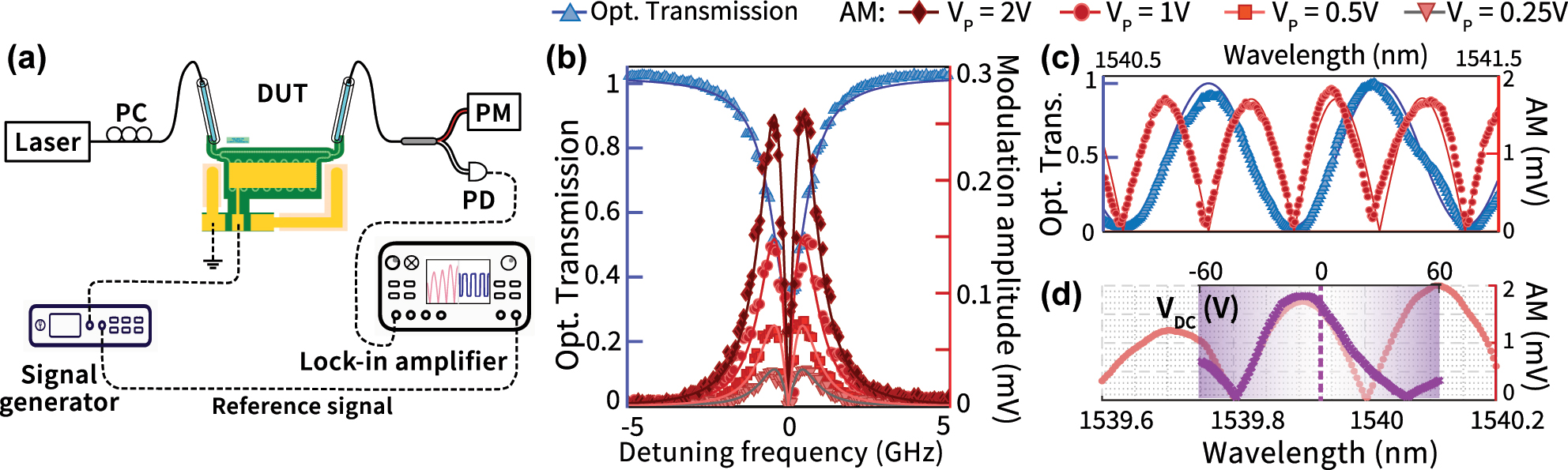
Characterization results. (a) Experimental setup used for electro-optic modulation characterization. (b) A representative mode from the normalized optical transmission spectrum (blue) of the racetrack EOM, showing a loaded quality factor Q ∼ 1.47 × 10⁵ and extinction depth ER = 4.83 dB (Supplementary Information, Section 3). The measured spectrum is fit using a Lorentzian lineshape (blue, solid). The measured modulation amplitude (lock-in signal) is shown (red, scatter) and the predicted fit is shown in shades of red for different applied modulation voltages ranging from 0.25 V to 2 V. We can see that the measured AM signal is clearly linear within this range. (c) A representative section of the optical transmission spectrum and modulation amplitude spectrum of the PeM-MZM device from Figure 2(a). The optical spectrum (blue scatter, normalized) is fitted with a sinusoidal curve (blue line), while the AM spectrum (red scatter) is fitted with a half-wave rectified sinusoidal model (red line). See Supplementary Information Section 4 for details on the fitting procedure. (d) AM spectrum of the PeM-MZM device measured with 0 V DC bias and 1 V RF voltage amplitude (pink scatter). Overlaid purple crosses show the AM response as the DC bias is swept from −60 V to 60 V (top x-axis) with the laser wavelength parked at the dashed line, and the RF signal amplitude fixed at 1 V. We believe the non-alignment of the data near λ = 1,540 nm is due to temperature induced spectral shifts during data acquisition.
Figure 3(b) and (c) shows the measured modulation amplitude spectra overlaid on the optical transmission spectra for the racetrack EOM and the PeM-MZM devices, respectively. The measured modulation amplitude as a function of laser wavelength agrees well with the gradient of the optical transmission spectra, in line with the PM to AM translation argument discussed above. Fitting the modulation amplitude (see Supplementary Information Section 4 for details) allow us to extract the modulation efficiency, expressed as a spectral tunability (η, [pm V−1]) or an equivalent half-wave voltage (V π ) need to shift the transmission from a maxima to a minima (or vice-versa). For racetrack EOMs with a loaded quality factor Q ≈ 1.47 × 10⁵ and extinction ratio ER = 4.83 dB, we extract an η = (0.351 ± 0.008) pm V−1 and a V π = (31.9 ± 0.8) V. For the PeM-MZM devices, the values are η = (0.139 ± 0.003) pm V−1 and a V π = (54.3 ± 1.3) V. The V π for PeM-MZM can also be directly quantified through a DC sweep measurement, as shown in Figure 3(d). Here, we repeat the modulation experiment as in Figure 3(a), but add a DC bias voltage on top of the AC voltage (amplitude = 1 V). By sweeping the DC bias voltage, one can in principle traverse the optical transmission spectrum, as shown in Figure 3(d), and read out the V π directly. The racetrack EOM measurement serves as a reference for the more complex PeM-MZM devices. From the modulation measurements, we can extract an equivalent refractive index change per unit applied voltage for both devices. This gives us Δn eff = 1.084 × 10⁻⁶ V−1 for racetrack EOM and Δn eff = 6.97 × 10⁻⁷ V−1 for PeM-MZM. The extracted Δn eff for the racetrack EOM agrees well with the predicted Δn eff = 1.279 × 10⁻⁶ V−1 using FEM simulation (cf. Supplementary Information Section 2).
We can also demonstrate the opposite phase shifts along the [011] and
![Figure 4:
Control experiments to demonstrate the push-pull nature of the effect: DC bias induced phase shift on two SeM-MZM devices, with a single arm meandering along [011] (i) or
[
01
1
̄
]
$[01\bar{1}]$
(ii) direction. The meandering arm lengths are designed to be nominally equal in the two cases. (a) AM spectra for SeM-MZMs driven by a 1 MHz modulation signal of amplitude 1 V, (blue for (i), red solid for (ii)). Overlaid scattered plot (red circles and blue triangles) shows the shift in the AM spectrum when the DC bias voltage is swept from 0 V (black dashed line) to 32 V. The laser wavelength is indicated by the dashed line (b) replotting the data from (a) to show the differential AM change as a function of applied DC bias voltage. The differential shift (ΔAM = AM(V
DC) − AM(0)) is plotted with reference to the zero DC bias point. The opposite slopes of the differential AM voltage with respect to the bias voltage V
DC
clearly shows the push-pull effect in action.](/document/doi/10.1515/nanoph-2025-0212/asset/graphic/j_nanoph-2025-0212_fig_004.jpg)
Control experiments to demonstrate the push-pull nature of the effect: DC bias induced phase shift on two SeM-MZM devices, with a single arm meandering along [011] (i) or
We measure the modulation bandwidth (BW) of the racetrack EOM and the PeM-MZM devices using a modified version of the setup shown in Figure 3(a). Here, we use a vector network analyzer (VNA, R&S ZVL) to drive (via Port 1) the device under test with a microwave signal (0 dBm, 225 mV RMS) and sweep the modulation frequency from 100 MHz to 9 GHz. The modulated signal is measured using a high-speed amplified photodiode (Optilab, APR-10-MC) whose output is fed back into the VNA (port 2) to perform a standard EO S 21 measurement. Figure 5(a) plots the normalized electro-optic frequency response of the racetrack (brown) and PeM-MZM (green) devices. The device response is normalized to 100 MHz, cf. Supplementary Information Section 5 for details on the normalization procedure. The extracted 3 dB modulation bandwidths of the racetrack EOM and PeM-MZM devices are ≈2 GHz and ≈0.8 GHz, respectively. In these proof-of-principle devices, the electrodes (see Figure 1(a)) were not optimized for high-speed operation, but more to ease fabrication constraints in order to demonstrate the push-pull effect in cm-scale devices. Therefore, our BW is primarily limited by the RC time constant of these lumped element electrodes. Figure 5(b) plots the measured electrode reflection S 11 spectra for the racetrack resonator and the PeM-MZM device. The wiggles apparent in the measured bandwidth (S 21) spectrum originate from a combination of the bare electrode response and the normalization procedure detailed in Supplementary Information Section 5. Supplementary Information Section 5 shows the extracted amplified photodiode gain spectrum which is non-monotonic and has an impact on the measured bandwidth spectrum.

Bandwidth measurements. (a) Measured (normalized) EO frequency response (S 21) for 2 cm long PeM-MZM (green) and racetrack EOM ring modulator (brown). The frequency response is normalized to 100 MHz and the normalization procedure is outlined in Supplementary Information Section 5. (b) Measured electrode reflection spectra (S 11) for the devices. The wiggles apparent in the bandwidth spectra (S 21) occur due to a combination of electrode reflection and photodiode gain normalization.
4 Discussion
While the results outlined in this paper clearly demonstrate the orientation dependent push-pull effect in the PeM-MZM devices, and the scale (2 cm suspended arm lengths in the MZI) shows the promise of bringing MEMS based nanofabrication approaches to integrated photonics platforms, the actual device performance leaves some scope for improvement. Many of the limitations in the EOM performance metrics outlined above can be traced to conservative design choices made on the nanofabrication side to get working devices. As noted above, the scale of these devices far exceeds what has been previously demonstrated in a suspended GaAs PIC platform [30], [31], coupled with the additional metallization constraints to generate the vertical field required at the waveguides.
Below, we outline how the various components of the PeM-MZM can be improved to achieve state-of-the-art modulator performance [23], [24], keeping in mind the trade-offs between increased device complexity and reduced fabrication yield. The three main components to improve are the underlying passive optical performance (insertion and propagation loss), improving the modulation efficiency and increasing the modulation bandwidth. We consider each in turn.
While we are clearly able to demonstrate the orientation-dependent push-pull effect using the PeM-MZM devices and achieve working EOMs, the underlying passive device optical performance needs improvement. In the device shown in Figure 2(a), we measure an end-to-end insertion loss of 29.8 dB, which we can sub-divide into 7.0 dB per grating coupler (2×), 1.0 dB per Y-splitter (2×) and 13.8 dB of propagation loss. Supplementary Information Section 3 provides further details on the loss extraction of the individual components. The optical propagation loss of 5.5 dB cm−1, extracted from the loaded quality factor of the racetrack resonators fabricated on the same chip, is 2.3× greater than the 2.4 dB cm−1 [35] that we have demonstrated in purely passive devices before.
The excess loss in the grating coupler is mainly due to an incomplete undercut of the underlying AlGaAs buffer layer. As noted in the fabrication procedure (Supplementary Information Section 1), we rely on a timed HF acid etch to remove the AlGaAs layer and suspend the waveguides. Given the lack of tensile stress in the GaAs device layer, overetching the buffer layer causes the membranes to sag [30] and given the scale of the devices (2.5 cm in each arm and 2 cm suspended sections), we were keen to prevent waveguide collapse with a view towards getting functional devices. Therefore, we restricted the (over)-etch time, and that resulted in an incomplete undercut of the AlGaAs sacrificial layer with the worst affected location being the grating coupler on account of its size, more specifically, the distance from the centre of the component to the nearest etch window. With process optimization, we should be able to achieve the loss metrics we have previously demonstrated [35] on these cm-scale devices. Moving to wider waveguide widths (≈750 nm) is a potential solution as it reduces surface loss while maintaining single-mode operation, although it comes at the cost of device footprint as the minimum bend radius increases from
The second area of improvement, is the optimization of top and bottom cladding thickness, and electrode design to maximize the refractive index change (Δn) per unit applied voltage and therefore maximize the modulation efficiency. In a vertical geometry like the GaAs EOM, the device can be approximated, to first order, as a series of three capacitors with dielectric constants roughly corresponding to the top cladding, waveguide and bottom cladding respectively. The voltage drop for such a series capacitor configuration scales inversely with the dielectric constant, which means a significant fraction of the field drops across the bottom air cladding. Both the top and bottom cladding thickness can be reduced by half to 1 µm from the current devices without affecting optical performance significantly, and ensuring higher electric field strengths for a given applied voltage. By moving to a top and bottom oxide cladding using conformal PECVD [42], we can improve the electric field strength by ≈3.3× and the overall Δn by ≈3.3×, cf. Figure 6. By building the same 2 cm PeM-MZM devices, we expect a V π ≈ 9.0 V. We would like to emphasize here that this optimization is performed keeping the GaAs device layer thickness fixed at 340 nm in keeping with standard silicon photonics foundry offerings. Increasing the thickness to 500 nm brings the V π down to ≈5.5 V for similar length devices. We would like to note that moving to a conformal PECVD reduces the index contrast and therefore mode confinement slightly, but this effect is very small in comparison to the increased field strength and associated increased modulation efficiency.
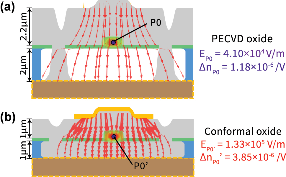
Electric field distribution comparison of the suspended GaAs waveguide devices shown in this work (a) with the proposed optimized geometry (b). Both the top and bottom cladding spacing to the electrodes can be reduced from ≈2 µm in the current devices to 1 µm without affecting optical performance. More importantly, by using conformal PECVD oxide deposition, the field strength at the waveguide (and the associated index change) can be significantly improved, as discussed in the main text. The FEM simulation of the local electric field strength is overlaid with optical mode and depicted using arrowheads that are scaled proportionally. Point P 0 locates the center of waveguide.
The final area of improvement to the devices reported in this work is incorporating travelling wave electrodes around the waveguides and velocity matching the microwave and optical fields with a view towards increasing the operational bandwidth. While the design of travelling wave electrodes is well-understood for GaAs [24], [43], adapting these designs to our tightly folded geometries while maintaining a low microwave insertion loss will require a re-optimization of the optical and microwave performance to maximize the device figure of merit. A second fabrication challenge that needs to be addressed is the thickness of the metal electrodes. To reduce the resistive loss at high frequencies, the metal thickness needs to be
5 Conclusions
We have demonstrated true push-pull electro-optic modulators in a suspended GaAs PIC platform by exploiting the orientation induced asymmetry of the Pockels r
41 coefficient and folding the two arms of an MZI along orthogonal crystal axes ([011] and [01
Funding source: Engineering and Physical Sciences Research Council
Award Identifier / Grant number: EP/N015126/1
Award Identifier / Grant number: EP/V052179/1
Award Identifier / Grant number: EP/X015300/1
Funding source: H2020 European Research Council
Award Identifier / Grant number: 758843
Acknowledgments
We would like to thank Laurent Kling, Stephen Clements, Robert Walker, Ian Farrer, Edmund Clarke and Andrew Murray for helpful suggestions and feedback.
-
Research funding: We gratefully acknowledge funding support from the UK’s Engineering and Physical Sciences Research Council (GASP, EP/V052179/1) and the European Research Council (ERC-StG, SBS 3-5, 758843). Nanofabrication was carried out using equipment funded by an EPSRC capital equipment grant (QuPIC, EP/N015126/1). The GaAs wafers were sourced from the UK’s national epitaxy facility in Sheffield (EP/X015300/1).
-
Author contributions: HL carried out the design, modelling, fabrication, and characterization of the devices with assistance from RT, PJ and KB. KB conceived and supervised the project. HL and KB wrote the manuscript with input from RT and PJ. All authors have accepted responsibility for the entire content of this manuscript and consented to its submission to the journal, reviewed all the results and approved the final version of the manuscript.
-
Conflict of interest: Authors state no conflict of interest.
-
Data availability: Data underlying the results presented in this paper are not publicly available at this time but may be obtained from the authors upon reasonable request.
References
[1] E. L. Wooten, et al.., “A review of lithium niobate modulators for fiber-optic communications systems,” IEEE J. Sel. Top. Quantum Electron., vol. 6, no. 1, pp. 69–82, 2000, https://doi.org/10.1109/2944.826874.Suche in Google Scholar
[2] M. Zhang, C. Wang, P. Kharel, D. Zhu, and M. Lončar, “Integrated lithium niobate electro-optic modulators: when performance meets scalability,” Optica, vol. 8, no. 5, pp. 652–667, 2021, https://doi.org/10.1364/optica.415762.Suche in Google Scholar
[3] J. Capmany and D. Novak, “Microwave photonics combines two worlds,” Nat. Photonics, vol. 1, no. 6, p. 319, 2007, https://doi.org/10.1038/nphoton.2007.89.Suche in Google Scholar
[4] X. Han, W. Fu, C.-L. Zou, L. Jiang, and H. X. Tang, “Microwave-optical quantum frequency conversion,” Optica, vol. 8, no. 8, pp. 1050–1064, 2021, https://doi.org/10.1364/optica.425414.Suche in Google Scholar
[5] K. C. Balram and K. Srinivasan, “Piezoelectric optomechanical approaches for efficient quantum microwave-to-optical signal transduction: the need for co-design,” Adv. Quantum Technol., vol. 5, no. 3, 2022, Art. no. 2100095, https://doi.org/10.1002/qute.202100095.Suche in Google Scholar
[6] J. Holzgrafe, et al.., “Cavity electro-optics in thin-film lithium niobate for efficient microwave-to-optical transduction,” Optica, vol. 7, no. 12, pp. 1714–1720, 2020, https://doi.org/10.1364/optica.397513.Suche in Google Scholar
[7] T. P. McKenna, et al.., “Cryogenic microwave-to-optical conversion using a triply resonant lithium-niobate-on-sapphire transducer,” Optica, vol. 7, no. 12, pp. 1737–1745, 2020, https://doi.org/10.1364/optica.397235.Suche in Google Scholar
[8] H. K. Warner, et al.., “Coherent control of a superconducting qubit using light,” arXiv preprint arXiv:2310.16155, 2023.Suche in Google Scholar
[9] T. A. Maldonado, “Electro-optic modulators,” in Handbook of Optics, vol. 2, 1995, pp. 13–11.Suche in Google Scholar
[10] C. Wang, et al.., “Ultrabroadband thin-film lithium tantalate modulator for high-speed communications,” Optica, vol. 11, no. 12, pp. 1614–1620, 2024, https://doi.org/10.1364/optica.537730.Suche in Google Scholar
[11] S. Abel, et al.., “Large Pockels effect in micro-and nanostructured barium titanate integrated on silicon,” Nat. Mater., vol. 18, no. 1, pp. 42–47, 2019, https://doi.org/10.1038/s41563-018-0208-0.Suche in Google Scholar PubMed
[12] PsiQuantum, et al.., “A manufacturable platform for photonic quantum computing,” Nature, vol. 641, no. 8064, pp. 876–883, 2025, https://doi.org/10.1038/s41586-025-08820-7.Suche in Google Scholar PubMed PubMed Central
[13] F. Kaufmann, G. Finco, A. Maeder, and R. Grange, “Redeposition-free inductively-coupled plasma etching of lithium niobate for integrated photonics,” Nanophotonics, vol. 12, no. 8, pp. 1601–1611, 2023, https://doi.org/10.1515/nanoph-2022-0676.Suche in Google Scholar PubMed PubMed Central
[14] R. D. V. Meade, S. G. Johnson, and J. N. Winn, Photonic Crystals: Molding the Flow of Light, New Jersey, Princeton University Press, 2008.10.1515/9781400828241Suche in Google Scholar
[15] K. Kawahara, et al.., “High-speed, low-voltage, low-bit-energy silicon photonic crystal slow-light modulator with impedance-engineered distributed electrodes,” Optica, vol. 11, no. 9, pp. 1212–1219, 2024, https://doi.org/10.1364/optica.531372.Suche in Google Scholar
[16] A. Nardi, et al.., “Integrated chirped photonic-crystal cavities in gallium phosphide for broadband soliton generation,” Optica, vol. 11, no. 10, pp. 1454–1461, 2024, https://doi.org/10.1364/optica.530247.Suche in Google Scholar
[17] M. Glick, L. Liao, and K. Schmidtke, Integrated Photonics for Data Communication Applications, Amsterdam, Elsevier, 2023.Suche in Google Scholar
[18] G. E. Hoefler, et al.., “Foundry development of system-on-chip InP-based photonic integrated circuits,” IEEE J. Sel. Top. Quantum Electron., vol. 25, no. 5, pp. 1–17, 2019, https://doi.org/10.1109/jstqe.2019.2906270.Suche in Google Scholar
[19] T. Kakitsuka, K. Hasebe, T. Fujii, T. Sato, K. Takeda, and S. Matsuo, “Inp-based membrane optical devices for large-scale photonic integrated circuits,” NTT Tech. Rev., vol. 13, no. 5, 2015, https://doi.org/10.53829/ntr201505ra1.Suche in Google Scholar
[20] J. J. van der Tol, et al.., “Indium phosphide integrated photonics in membranes,” IEEE J. Sel. Top. Quantum Electron., vol. 24, no. 1, pp. 1–9, 2017, https://doi.org/10.1109/jstqe.2017.2772786.Suche in Google Scholar
[21] Y. Wang, Y. Jiao, and K. Williams, “Scaling photonic integrated circuits with inp technology: a perspective,” APL Photonics, vol. 9, no. 5, 2024, https://doi.org/10.1063/5.0200861.Suche in Google Scholar
[22] Y.-C. Wang, “GaAs foundry technologies,” in Proceedings of Technical Program-2014 International Symposium on VLSI Technology, Systems and Application (VLSI-TSA), IEEE, 2014, pp. 1–2.10.1109/VLSI-TSA.2014.6839698Suche in Google Scholar
[23] N. Dagli, “Wide-bandwidth lasers and modulators for RF photonics,” IEEE Trans. Microwave Theory Tech., vol. 47, no. 7, pp. 1151–1171, 1999, https://doi.org/10.1109/22.775453.Suche in Google Scholar
[24] R. G. Walker, N. I. Cameron, Y. Zhou, and S. J. Clements, “Optimized gallium arsenide modulators for advanced modulation formats,” IEEE J. Sel. Top. Quantum Electron., vol. 19, no. 6, pp. 138–149, 2013, https://doi.org/10.1109/jstqe.2013.2266321.Suche in Google Scholar
[25] R. Walker, N. Cameron, Y. Zhou, C. Main, G. Hoy, and S. Clements, “50GHz gallium arsenide electro-optic modulators for spaceborne telecommunications,” in International Conference on Space Optics – ICSO 2018, vol. 11180, SPIE, 2019, pp. 2683–2691.10.1117/12.2536187Suche in Google Scholar
[26] P. Lodahl, S. Mahmoodian, and S. Stobbe, “Interfacing single photons and single quantum dots with photonic nanostructures,” Rev. Mod. Phys., vol. 87, no. 2, pp. 347–400, 2015, https://doi.org/10.1103/revmodphys.87.347.Suche in Google Scholar
[27] N. Tomm, et al.., “A bright and fast source of coherent single photons,” Nat. Nanotechnol., vol. 16, no. 4, pp. 399–403, 2021, https://doi.org/10.1038/s41565-020-00831-x.Suche in Google Scholar PubMed
[28] J. R. Scott and K. C. Balram, “Timing constraints imposed by classical digital control systems on photonic implementations of measurement-based quantum computing,” IEEE Trans. Quantum Eng., vol. 3, pp. 1–20, 2022. https://ieeexplore.ieee.org/document/9779088.10.1109/TQE.2022.3175587Suche in Google Scholar
[29] K. Alexander, et al.., “A manufacturable platform for photonic quantum computing,” arXiv preprint arXiv:2404.17570, 2024.Suche in Google Scholar
[30] P. Jiang and K. C. Balram, “Suspended gallium arsenide platform for building large scale photonic integrated circuits: passive devices,” Opt. Express, vol. 28, no. 8, pp. 12262–12271, 2020, https://doi.org/10.1364/oe.385618.Suche in Google Scholar PubMed
[31] A. Khurana, P. Jiang, and K. C. Balram, “Piezo-optomechanical signal transduction using lamb-wave supermodes in a suspended gallium arsenide photonic-integrated-circuit platform,” Phys. Rev. Appl., vol. 18, no. 5, 2022, Art. no. 054030, https://doi.org/10.1103/physrevapplied.18.054030.Suche in Google Scholar
[32] E. J. Stanton, et al.., “Efficient second harmonic generation in nanophotonic GaAs-on-insulator waveguides,” Opt. Express, vol. 28, no. 7, pp. 9521–9532, 2020, https://doi.org/10.1364/oe.389423.Suche in Google Scholar PubMed
[33] G. Roelkens, et al.., “Present and future of micro-transfer printing for heterogeneous photonic integrated circuits,” APL Photonics, vol. 9, no. 1, 2024, https://doi.org/10.1063/5.0181099.Suche in Google Scholar
[34] S. Mookherjea, V. Mere, and F. Valdez, “Thin-film lithium niobate electro-optic modulators: to etch or not to etch,” Appl. Phys. Lett., vol. 122, no. 12, 2023, https://doi.org/10.1063/5.0142232.Suche in Google Scholar
[35] R. Thomas, H. Li, J. Laverock, and K. C. Balram, “Quantifying and mitigating optical surface loss in suspended GaAs photonic integrated circuits,” Opt. Lett., vol. 48, no. 15, pp. 3861–3864, 2023, https://doi.org/10.1364/ol.492505.Suche in Google Scholar
[36] Ž. Zobenica, et al.., “Integrated nano-opto-electro-mechanical sensor for spectrometry and nanometrology,” Nat. Commun., vol. 8, no. 1, p. 2216, 2017, https://doi.org/10.1038/s41467-017-02392-5.Suche in Google Scholar PubMed PubMed Central
[37] R. Walker, “High-speed electrooptic modulation in GaAs/GaAlAs waveguide devices,” J. Lightwave Technol., vol. 5, no. 10, pp. 1444–1453, 1987, https://doi.org/10.1109/jlt.1987.1075432.Suche in Google Scholar
[38] N. Dagli, “III-V compound semiconductor electro-optic modulators: chapter 4,” in High-Speed Photonic Devices, Ch. 4, Taylor & Francis, 2007, pp. 63–108.10.1201/9781420012071.ch4Suche in Google Scholar
[39] L. Midolo, et al.., “Electro-optic routing of photons from a single quantum dot in photonic integrated circuits,” Opt. Express, vol. 25, no. 26, pp. 33514–33526, 2017, https://doi.org/10.1364/oe.25.033514.Suche in Google Scholar
[40] M. Cherchi, S. Ylinen, M. Harjanne, M. Kapulainen, and T. Aalto, “Dramatic size reduction of waveguide bends on a micron-scale silicon photonic platform,” Opt. Express, vol. 21, no. 15, pp. 17814–17823, 2013, https://doi.org/10.1364/oe.21.017814.Suche in Google Scholar
[41] N. Quack, et al.., “MEMS-enabled silicon photonic integrated devices and circuits,” IEEE J. Quantum Electron., vol. 56, no. 1, pp. 1–10, 2019, https://doi.org/10.1109/jqe.2019.2946841.Suche in Google Scholar
[42] J. R. Abelson and G. S. Girolami, “New strategies for conformal, superconformal, and ultrasmooth films by low temperature chemical vapor deposition,” J. Vac. Sci. Technol., A, vol. 38, no. 3, 2020, https://doi.org/10.1116/6.0000035.Suche in Google Scholar
[43] J. Shin, C. Ozturk, S. Sakamoto, Y. Chiu, and N. Dagli, “Novel t-rail electrodes for substrate removed low-voltage high-speed GaAs/AlGaAs electrooptic modulators,” IEEE Trans. Microwave Theory Tech., vol. 53, no. 2, pp. 636–643, 2005, https://doi.org/10.1109/tmtt.2004.840735.Suche in Google Scholar
[44] P. S. Kuo, J. Bravo-Abad, and G. S. Solomon, “Second-harmonic generation using-quasi-phasematching in a GaAs whispering-gallery-mode microcavity,” Nat. Commun., vol. 5, no. 1, p. 3109, 2014, https://doi.org/10.1038/ncomms4109.Suche in Google Scholar PubMed PubMed Central
[45] M. Jankowski, et al.., “Ultrafast second-order nonlinear photonics – from classical physics to non-Gaussian quantum dynamics: a tutorial,” Adv. Opt. Photonics, vol. 16, no. 2, pp. 347–538, 2024, https://doi.org/10.1364/aop.495768.Suche in Google Scholar
Supplementary Material
This article contains supplementary material (https://doi.org/10.1515/nanoph-2025-0212).
© 2025 the author(s), published by De Gruyter, Berlin/Boston
This work is licensed under the Creative Commons Attribution 4.0 International License.
Artikel in diesem Heft
- Frontmatter
- Research Articles
- Direct measurement of two-photon absorption and refraction properties of SZ2080TM-based resists at 515 nm: insights into 3D printing
- Exploring 2D-LIPSS formation under circular polarization in ultrafast laser processing
- Enhancement of second-harmonic generation through Brillouin zone folding in a waveguide-coupled metasurface
- Efficient and tunable frequency conversion using periodically poled thin-film lithium tantalate nanowaveguides
- Efficient high-quality photon pair generation in modal phase-matched thin-film lithium niobate micro-ring resonators
- Engineering cm-scale true push-pull electro-optic modulators in a suspended GaAs photonic integrated circuit platform by exploiting the orientation induced asymmetry of the Pockels r 41 coefficient
- Cascades of quasi-bound states in the continuum
- Dual-mode varifocal Moiré metalens for quantitative phase and edge-enhanced imaging
- Frequency-multiplexed optical reservoir computing using a microcomb
- Self-accelerating topological edge states
- Letter
- Rapid adiabatic couplers with arbitrary split ratios for broadband DWDM interleaver application