Transferring diffractive optics from research to commercial applications: Part II – size estimations for selected markets
-
Robert Brunner


Abstract
In a series of two contributions, decisive business-related aspects of the current process status to transfer research results on diffractive optical elements (DOEs) into commercial solutions are discussed. In part I, the focus was on the patent landscape. Here, in part II, market estimations concerning DOEs for selected applications are presented, comprising classical spectroscopic gratings, security features on banknotes, DOEs for high-end applications, e.g., for the semiconductor manufacturing market and diffractive intra-ocular lenses. The derived market sizes are referred to the optical elements, itself, rather than to the enabled instruments. The estimated market volumes are mainly addressed to scientifically and technologically oriented optical engineers to serve as a rough classification of the commercial dimensions of DOEs in the different market segments and do not claim to be exhaustive.
1 Introduction
In the last decade, the topic of diffractive optics experienced a continuous shift from basic research toward its commercial exploitations. In a series of two contributions, we discuss selected and decisive business-related aspects of the current status of this transfer process. In a preceding issue of this journal [1], the development of the patent landscape in diffractive optics was discussed showing a recent significant patent offensive by Japanese companies, e.g., especially in the field of imaging diffractive optical elements (DOEs).
Here, in this paper, we present estimations of the market volumes concerning DOEs for selected applications. The contribution addresses mainly scientifically and technologically oriented optical engineers with experiences in academic research, in particular, also graduate and PhD students to offer them an insight into the commercial world and to promote a basic market understanding. In this regard, the intention is to improve the interaction between university and industry.
The selected markets cover a broad diversity in using DOEs, ranging from high-end to high-volume applications. Hereby, all enabling optical characteristics of DOEs such as imaging, beam shaping, coherence forming, or dispersive characteristics are involved. In particular, the selected topics comprise security features on banknotes, DOEs for high-end applications, e.g., for the semiconductor manufacturing market and diffractive intra-ocular lenses. As a reference, diffractive gratings for spectroscopy are mentioned, as well.
The estimated market volumes intend to serve as a rough overview and classification of the commercial importance of DOEs in the different market segments and allow a comparison of the market penetration of the different diffractive optical approaches. It has to be mentioned that the numbers given here do not claim to be exhaustive as it would be necessary, e.g., as a base for a robust business plan. But, the evaluated magnitude of business ranges allows an indication of the employment level for optical engineers in the related fields.
The consideration of current commercial aspects also allows a review of the original expectations of diffractive optics, especially which of them were fulfilled, which fell short and which exceeded the original anticipations. It has become clear that some DOE characteristics, which were originally assumed to have a strong impact in potential products, did not fulfill the expectations, whereas some others experienced an unexpected success. The discrepancy between former expectations and reality may also be attributed to a gap between scientific interest and economic importance for the spectrum of the DOE applications.
The derived market estimations are solely referred to the optical elements, itself, and not to the enabled instruments, which benefit directly from the added value. This approach is essential, especially for profit center-organized production units, which needs to work cost effective for every manufactured element. In such a business model, a potential financial deficiency in the production of the elements, themselves, cannot be compensated through the final system or product.
Certain fundamental optical tasks, such as beam shaping or beam homogenization, can be treated with either diffractive or refractive micro-optical components, and moreover, in some cases, the functionality of a micro-optical element combines both diffractive and refractive working principles so that a clear differentiation is not possible. Therefore, and also due to partly similar or equivalent methods to manufacture diffractive and refractive micro-optical components, in our market considerations, we have partly included refractive micro-optical elements, such as refractive diffusers or microlens arrays.
2 Classical spectroscopic gratings
Gratings for spectroscopy represent the market with the longest history in the field of micro-structured elements. Diffractive gratings are the key components for laboratory-used spectrometers and currently are broadening the application area to fields such as agri-food industry, biomedical engineering, or as devices for in-line and at-line process control for production technologies. The basic technologies to manufacture diffractive gratings comprise the mastering, e.g., with classical ruling or interference lithography and the replication process in which the master element is transferred into thermal- or UV-curable resins.
The market for these elements is addressed by companies such as Jobin Yvon, Carl Zeiss, Newport Corporation (Richardson Gratings), Lightsmyth, Headwall, Spectrogon, or Shimadzu. According to estimates from experts and product managers acting in this field, the total sales volume per year for these elements, themselves, is approximately €50Mio (2010). Hereby, high-end gratings for space or astronomical applications, and also, gratings for the use in synchrotron beam-lines are excluded. For spectroscopic sensor systems, a stable market is expected for the next years with an annual growth rate between 6% and 9% [2]. For miniaturized and portable devices, a much higher growth rate of up to 20% is expected [3].
3 Diffractive- and micro-optical structures as security features on banknotes
In the continuous race against the counterfeiter of banknotes, the ‘money makers’ permanently have to improve their security features and protection items. Hereby, the appropriate security features should allow, on the one hand, a simple visual verification, and on the other hand, it has to guarantee high degrees of difficulties to copy or counterfeit. For these applications, diffractive and other micro-optical structures have already demonstrated their enormous usability and also offer a high potential for future improvements. Examples of currently applied micro-optical security structures on banknotes are holograms, diffractive security threads, and optically variable devices (OVDs) such as security holograms, e.g., so-called ‘kinegrams’, or latent image effects (‘kipp effects’), which change color with changing viewpoint or where pictures on the banknote appear, disappear, or switch into negative when the observation angle is varied. In addition, refractive microlens-based features are implanted in modern banknotes, which provide characteristic moving effects. As an example, Figure 1 shows photographs of a detail of the new €5 banknote illuminated with white light under different angles. The color change in the different zones due to diffractive effects is clearly visible.
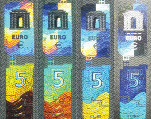
Diffractive structures on the €5 banknote. Four photographs were taken from a detail of the banknote. From one shot to the next, the incidence angle was changed so that different colors are perceived for the same areal position.
Although the application of micro-optical structures on banknotes seems to be very different compared to classical requirements in imaging or illumination systems of optical instruments, many aspects of both are absolutely comparable. Especially, the basic manufacturing technologies are often identical. In both, high-volume products for the optical industry and also for the making of banknotes, multistep processes are necessary, which in general comprise the mastering process of the original micro-structured element, the manufacturing of the replication tool, and finally the replication process itself. For instance, for the mastering process used for banknote printing, also e-beam and laser lithography are relevant technologies. Of course, the replicated numbers, which are typical for ‘classical’ optical products and banknotes, differ in dimensions.
The estimated numbers of banknotes in circulation worldwide vary between 200 bn1 and 375 bn, and about 40% of the total number is related to new production in each year [4–7]. The relatively high number of new production is mainly related to the necessary replacement of banknotes with heavy signs of wear or damage. The life period of a banknote ranges from some months to several years depending on the quality of the banknote and also on the environmental conditions, e.g., the humidity where it is in use.
In order to guarantee the highest level of security and independency, most countries operate their own banknote manufacturing in highly controlled government printing offices. That means, the worldwide market of banknote printing is a rather closed business, and only 12%–18% of the market is freely accessible. Major players in this free market are companies such as de la Rue (GB), Giesecke & Devrient (D) or Oberthur (F).
The production cost of a banknote depends strongly on the required quality and amounts, i.e., approximately $43/1000 units for US-Dollar banknote and about 10–15 Euro-cent for a Euro-note. As a critical and highly decisive component on a banknote, the micro-optical security features (including security thread) covers approximately a value percentage of ˜5–20% of the entire production cost, which leads to a share of about 0.5–3 cent/banknote. With this estimation and assuming a global market of 200 bn banknotes per year, for micro-optical security features on banknotes, a market size between €1 bn and €6 bn results. If only the free accessible market with approximately 20 bn units/year is taken into account, still a total value between €100 Mio and €600 Mio is addressable.
In this market of banknote printing, some significant future trends can be identified. For example, the lifetime of banknote becomes an essential factor, which leads to potential material switch from classical cotton-based ‘paper’ to polymers. Hereby, it is assumed that polymer notes will last 3.5 times longer than paper notes. In combination with polymer substrates, a larger area for micro-optical security features will be available. This may lead to an increase in the value percentage of micro-optical features up to 5–7 cent/banknote, especially for higher-valued banknotes.
4 Market for high-performance optical instruments
The market for high-performance optical instruments comprises the classical professional market and the high-end, premium consumer segment. Here, typical representatives of the professional market are optical- or laser-based production machines, high-end microscopes, or optical instruments for medical diagnostics and therapy. High-performance binoculars, spotting scopes, photo camera, and lens systems are classical examples for the premium-consumer market.
The business of high-performance optical instruments is typically characterized by moderate or minor quantities of traded systems and by a relatively high individual system prize. In general, the relevant high-performance systems are composed of several crucial and indispensable submodules, in which a high number of opto-mechanical elements are integrated. That means, there is not only one single important element, which decides above the success of the instrumental system, but several elements offering an ‘enabling’ function. From this follows that, although the system prize for a high-performance systems is high, the single element (e.g., a micro-optical element) is still exposed to an intensive cost pressure. Additionally, due to the limited number of systems sold per year, often the business volume with specific elements, such as diffractive or other micro-optical components, is rather moderate. For example, for high-end camera systems, e.g., with an integrated imaging diffractive optical element, a few thousand systems are sold per year with a typical trading price of a few thousand Euros. Following the previous argumentation, the component prize, e.g., for the diffractive lens, has to be limited to several tens up to a few hundred Euros. This implies that for the single element, a total volume of €1–3 Mio/year can be expected. These quantities have to be opposed to the efforts and costs necessary to develop a new production technology for micro-optical elements and immediately reveal the financial difficulties for their introduction.
Other examples in which micro-optical elements are used as enabling elements in professional optical systems concern excimer-laser applications. Currently, from the view point of the financial volume and with the exception of semiconductor manufacturing industry, the most dominant applications for excimer-lasers are flat panel display manufacturing and refractive eye surgery. Figure 2 shows the color-coded height profiles of a diffractive (left) and a refractive (right) micro-optical element used as tailored diffusers, which find application in refractive eye surgery.
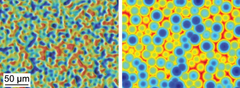
Color-coded height profiles of diffractive (left) and refractive (right) micro-optical diffusers.
For the above-mentioned applications, the prize of decisive optical elements varies between €600–800 (eye surgery) and €1000–1500 (display manufacturing). Taking also the numbers for the systems sold per year into account, a volume of a few million Euros for the micro-optical component can be estimated.
5 Semiconductor manufacturing industry (microlithography)
The all-dominant driving force in semiconductor manufacturing industry is the relentless quest to permanently decrease the feature size of integrated circuits (ICs) such as logic or memory devices from one product generation to the next. The core technology of the semiconductor manufacturing process is microlithography with highly sophisticated steppers and scanners as the working horses. In these tools, the structures of a mask are projected into the wafer plane to expose the photoresist. Steppers and scanners belong worldwide to the systems with highest standards in quality of all optical instruments. In microlithography, a bundle of approaches are addressed to realize small structure sizes, which are, in the meanwhile, in the production process in the 20-nm range. Some of the most important factors in the microlithographic process are the short working wavelength (193 nm), a projection lens system with very high numerical aperture, which is currently achieved with water immersion systems, and sophisticated mask features such as optical proximity corrections (OPCs) or phase structures.
In addition to the projection lens, a further highly important part of a stepper or a scanner is the illumination system, which also plays an important role to decrease the feature sizes on the wafer. The illumination system has several essential functionalities. A main aspect concerns the necessity of a highly uniform illumination of the mask area, which has to be projected into the wafer plane. The uniform mask illumination is realized by a ‘homogenizer’ in the illumination system. A further extremely crucial aspect concerns the light distribution in the pupil plane of the illumination system. The light distribution in the pupil plane is directly transferred by the condenser optics into an angle distribution of the light field illuminating the addressed mask area. The incidence angles of the incoming light field strongly determine the interaction with the mask features and, therefore, contribute significantly to the resolution of the lithographic process. That means the illumination system of a stepper or scanner has to enable specific light distributions in the pupil plane such as ring-shaped, dipole, or quadrupole profiles or even more complex structures. Actually, for specific high-end applications, the pupil filling has to be customized individually for the applied mask or both mask structures, and pupil filling is optimized simultaneously in an interactive process. To fulfill the demands for pupil shaping and field uniformity, a number of diffractive and micro-optical elements are applied in the illumination systems of steppers/scanners. Typical elements are computer-generated holograms (CGHs) for pupil shaping, refractive and diffractive diffusers, coherence-forming elements, and microlens arrays as field homogenizers. Owing to the high optical performance and the need to reduce the waste of photons to a minimum, the specifications of these micro-optical elements are extremely ambitious and, in general, very close to the achievable physical limit.
The market of the diffractive and refractive micro-optical devices used in semiconductor manufacturing industry is directly coupled to the business fluctuations of the steppers and scanners, themselves. Figure 3 shows the yearly unit numbers of lithography tools for IC industry shipped worldwide between 2004 and 2012 [8–10]. From 2004 to 2007, around 600 units per year were delivered followed by a sharp decay with a minimum of 128 units/year in 2009. Meanwhile, the semiconductor market experienced a recovery, and the numbers of the shipped IC steppers and scanners increased to a value of 376 units in 2011 and 270 units in 2012, respectively. The pure number of shipped units per year is not the only crucial factor of the lithography tool business but also, e.g., the development of the selling price of steppers and scanners has to be taken into account. Currently, for low-end products, such as i-line steppers, the average selling price is approximately $5 Mio [8]. On the other hand, the market sells dry ArF systems (non-immersion) for more than $15 Mio. The highest price for production tools is currently paid for ArF immersion tools that sell for more than 30 Mio$ [8]. To differentiate the shipping numbers between low-end and high-end tools in more detail, the inset of Figure 3 shows a closer view of the concrete distribution for the reference year 2011 [8, 11]. Here, low-end and high-end contributions are further segmented into the parts of the companies ASML, Nikon, and Canon, the only three players serving the lithography tool market.
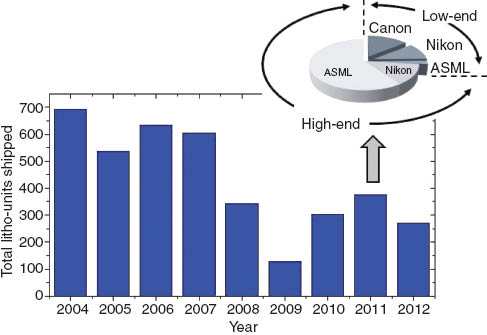
Unit numbers of lithography tools (steppers/scanners) for the IC industry shipped worldwide between 2004 and 2012. The inset shows the distribution between high-end and low-end systems and also the percentage for the three players serving the lithography tool market. The reference year was 2011.
In 2011, approximately 375 units were shipped worldwide, whereas about 100 tools contribute to low-end systems (e.g., i-line or KrF systems), and the majority of the 275 units are high-end scanners (ArF immersion). The Dutch company ASML is the market leader with an overall share on unit basis of 57%. The Japanese companies Nikon and Canon cover 28% of the market and 15%, respectively. The high-end market is absolutely dominated by ASML with a share of 82% in 2011 and 18% for Nikon. Canon, which does not contribute to the high-end segment, is the market leader for low-end systems with 53%. In the low-end market Nikon shares 40%, and ASML, 8%, respectively.
From these numbers, the market size for diffractive and refractive micro-optical components used for IC steppers and scanners can also be estimated. Assuming between 300 and 400 stepper and scanner units shipped per year and further assuming that for each lithography tool between 10 and 20 micro-optical elements are integrated with an average price between €5 k and €20 k, a total market volume for micro-optical elements of approximately €50 Mio –€90 Mio can be estimated. Players in this market of high-performance micro-optical elements for litho tools are companies such as Suss Microoptics [12], Lissotschenko Mikrooptik (LIMO) [13], Carl Zeiss [14], Jenoptik [15], Tessera (DOC) [16], or Natsume [17].
In recent years, a particular aspect in the application of micro-optical elements for illumination systems of scanners concerned the previously mentioned use of customized individual pupil fillings for specific photo mask features. The need for the simultaneous optimization of pupil filling and mask features means that for each of the relevant masks, a specific CGH has to be manufactured. This necessity increased significantly the demand for high-end diffractive elements. Unfortunately, for the providers of micro-optical components, the manufacturer of lithography tools has found, in the meanwhile, an alternative, which allows a flexible and adjustable pupil filling in the scanner illumination system without the need of permanently new CGHs. These technical solutions are associated with the keywords ‘FlexRay’ (ASML) or ‘flexible pupilgram creation’ (Nikon). Although, for the illumination of the flexible pupil generator, also micro-optical elements are necessary, the total number of micro-optical elements is reduced due to the decrease in the demand for customized CGHs.
6 Intra-ocular lenses
Cataract is a clouding of the eye’s natural crystalline lens, which degrades visual acuity. Cataracts are mainly associated with biological aging so that this disease is very common in older people. The number of people affected by cataracts increases from about 4% of the population between 50 and 59 years, to more than 60–70% of those aged 90 years and older. To help the affected patients, cataract surgeries are carried out, which are, worldwide, one of the most often performed operations. In cataract surgery, the natural crystalline lens is replaced by an artificial clear intra-ocular lens (IOL).
Owing to the widespread distribution of cataracts, the market for IOLs is enormous. Currently, the main driving forces for the increase in the IOL market are the aging society and the economic growth in the emerging markets, which also improve the access to medical treatment for their population. The available artificial IOLs can be distinguished in their functionalities. The most common IOLs are conventional refractive lenses, in which the optical power is determined by the radius of curvature of the two limiting spherical surfaces and the refractive index of the material. In fact, these IOLs allow, in principle, a clear vision but are limited in the functionality to only one fixed focus position. That means, after the surgery, the eye of patient is only corrected for a fixed distance. Especially, accommodation, the ability for flexible adjustment of the lens to adapt for near or far vision, is not possible. To overcome this limitation, alternative IOL concepts were developed, which address the premium segment of the IOL market. Especially, the so-called multifocal IOLs offer, in addition to the opacity correction, the possibility to perceive simultaneously the far, near, and intermediate range.
The working principle of these multifocal IOLs is based on a diffractive optical approach. The two or three foci are either realized by using different diffraction orders or by superposing or interleaving diffraction structures where each is acting in specific diffraction orders. Figure 4 shows an exemplary diffractive multifocal IOL (AT LISA tri 839MP; Carl Zeiss Meditec AG) with the clearly visible concentric ring system (Figure 4, right) and displays schematically the basic working principle. Objects from three different distances to the eye are focused simultaneously on the retina, where different diffraction orders are used (Figure 4, left).
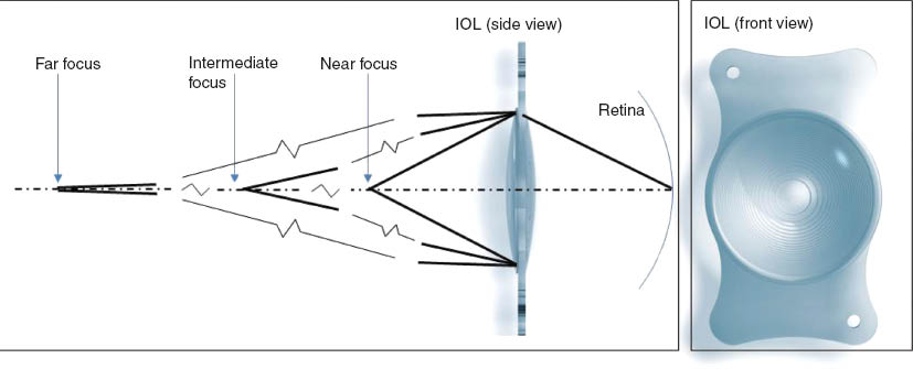
(Left) Schematic illustration of the basic working principle of a diffractive intra-ocular lens. Objects from three different distances to the eye are focused simultaneously on the retina, where different diffraction orders are used. (Right) Front view of an exemplary diffractive multifocal IOL with clearly visible concentric ring system (Courtesy of Carl Zeiss Meditec AG).
In comparison to the previous discussed businesses of optical elements, the global IOL market is enormous and was valued at $2.7 bn in 2008 [18], and is expected to reach $3.98–4.3 bn by 2017 [19, 20]. Here, the market growth relates to both the wealthy nations and also the developing countries.
The estimated market development of the multifocal IOLs in the premium market is depicted in Figure 5. As a base served the US market numbers for IOLs in 2010. Here, the total IOL market was valued at $775 Mio [21] where 39% of the total IOL revenue contributed to the premium market [22]. The annual growth rate in the premium segment is expected by experts to be in the order of 10% or even higher [23, 24]. The bar graph in Figure 5 displays the derived worldwide growth for multifocal IOLs following the conservative assumption that world market for these elements is, in minimum, twice the US market and expecting a 10% growth rate. For comparison, the upper and lower curves in Figure 5 represent the estimations for 8% and 12% growth rates, respectively, assuming slightly higher (or resp. lower) starting values. From this, it follows that the current global market size of multifocal IOLs range between €450 and 600 million per year and is expected to grow up to €680 Mio, or even higher, up to values larger than €1 bn in 2018.
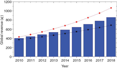
Expected development of the multifocal IOLs in the premium market segment. The bar graph displays the estimated worldwide growth for multifocal IOLs assuming a 10% growth rate. For comparison, the upper (red) and lower (black) curves represent the estimations for 8% and 12% growth rates, respectively, assuming slightly higher (or, respectively, lower) starting values.
Multifocal IOLs provide simultaneously two or three foci for sharp vision of different distant objects. On the other hand, multifocal IOLs are also negatively known to reduce contrast sensitivity and cause glare disability or introduce halo effects. That means, after cataract surgery, the optimum solution for a patient is not a diffractive-based IOL but would be a monofocal IOL with self-accommodative ability. Currently, large effort is being made in the research and development of different approaches for those accommodative IOLs, so that their introduction may squeeze the multifocal competitor out of the market. At the moment, the implementation success of accommodating lenses is limited, e.g., by the occurrence of capsular opacification due to lens epithelial cell growth or by the loss of the flexibility of the accommodative mechanism due to capsular fibrosis. That means, although it is likely that full accommodative IOLs will replace diffractive multifocal IOLs some days, it is expected that this transition takes several years, perhaps a decade or more. In the interim time, diffractive-based multifocal IOLs may control this market.
7 Conclusion
In the preceding sections, a limited and subjective, but also representative, selection of different market segments in the context of ‘diffractive optics’ was presented, and their business volumes were discussed. The comparison shows a broad diversity in the business volumes in the different market segments considered here, in which the difference covers several orders of magnitude. In some of these market segments, diffractive optics shows already a significant market success. As it is often the case, this is true for the high-volume market with the example of multifocal intra-ocular lenses and the highest-quality market with the example of diffractive optics for semiconductor manufacturing industry. In other market segments, it seems to be hard to justify the necessary investments for the introduction of new manufacturing technologies. But still in the latter case, a business success can be expected, not by the DOE, itself, but indirectly by using DOEs as enabling elements for the introduction of new systems offering performance and functionalities, which cannot be fulfilled without them. This assumption correlates to the strong, currently growing patent activities especially of the Japanese companies in the field of ‘diffractive optics’ [1]. Although the market size for single elements seems to be small for the addressed application fields, such as microscopy or high-end telephoto lenses, the current activities of the involved companies show that new products based on DOEs can probably be expected in the near future.
- 1
Billion, bn=109
Very special thanks are due to Mario Gerlach from the Carl Zeiss Meditec AG (Berlin) for his valuable support concerning the IOL topic. The work was financially supported by the German Research Foundation DFG within the Priority Program ‘Active Micro-optics’ and the Thuringia Ministry of Education, Science and Culture (TMBWK FKZ 11015-514; ‘AKMOSYS’).
References
[1] R. Brunner, Adv. Opt. Technol. 2(5–6), 351–359 (2013).Suche in Google Scholar
[2] D. Walsh, ‘Market Trends and Closing Remarks’; oral presentation at SPIE Spectroscopy Technology + Applications; Boston (MA, USA) 03.11.2008.Suche in Google Scholar
[3] A. Whitely, ‘Spectroscopy: Imagine All the People Using Raman Today and Tomorrow’ oral presentation at SPIE Spectroscopy Technology + Applications; Boston (MA, USA) 03.11.2008.Suche in Google Scholar
[4] Giesecke & Devrient; http://www.gi-de.com/usa/en/index.jsp; accessed on 09.09.2013.Suche in Google Scholar
[5] http://www.madehow.com/Volume-3/Paper-Currency.html#ixzz2RyvO4CMK; accessed on 09.09.2013.Suche in Google Scholar
[6] J. Brühl, ‘Wo das Geld wächst; Süddeutsche Zeitung, 15.5.2012, online http://sz.de/1.1348871, accessed on 14.01.2014.Suche in Google Scholar
[7] K. W. Bender, ‘Moneymakers: The Secret World of Banknote Printing’ (Wiley-VCH Weinheim, Germany, 2006).Suche in Google Scholar
[8] http://www.siliconsemiconductor.net/article/74993-Can-Nikon-or-Canon-Ever-Catch-ASML-in-the-Lithography-Market.php; accessed on 14.11.2013.Suche in Google Scholar
[9] http://www.asml.com/asml/show.do?lang=EN&ctx=48039&dfp_fragment=ifrs_semiconductor_equipment_industry; accessed on 14.11.2013.Suche in Google Scholar
[10] http://www.asml.com/asml/show.do?ctx=39585&rid=39590; accessed on 14.11.2013.Suche in Google Scholar
[11] http://www.eetimes.com/document.asp?doc_id=1261461; accessed on 14.11.2013.Suche in Google Scholar
[12] http://www.suss-microoptics.com/; accessed on 14.11.2013.Suche in Google Scholar
[13] http://www.limo.de/en/home/; accessed on 14.11.2013.Suche in Google Scholar
[14] http://czjena.zeiss.com/carl-zeiss-jena/en_de/capabilities/optical-components/microoptics.html; accessed on 14.11.2013.Suche in Google Scholar
[15] http://www.jenoptik.com/en-microoptics; accessed on 14.11.2013.Suche in Google Scholar
[16] http://www.doc.com/Pages/home.aspx; accessed on 14.11.2013.Suche in Google Scholar
[17] http://www.mflens.co.jp/en/products/drum_lensflyeye_lens.html; accessed on 14.11.2013.Suche in Google Scholar
[18] http://www.prlog.org/10272418-intra-ocular-lens-iol-pipeline-technology-and-market-forecasts-to-2015.html; accessed on 14.11.2013.Suche in Google Scholar
[19] http://www.prweb.com/releases/intraocular_lenses_IOL/hard_foldable_lenses/prweb9273925.html; accessed on 14.11.2013.Suche in Google Scholar
[20] http://market-scope.com/wp-content/uploads/2012/07/IOL-graphic.png; accessed on 14.11.2013.Suche in Google Scholar
[21] http://www.marketresearch.com/GlobalData-v3648/Intraocular-Lens-IOL-Global-Pipeline-6744372/; accessed on 15.01.2014.Suche in Google Scholar
[22] https://www.asdreports.com/news.asp?pr_id=275; accessed on 15.01.2014.Suche in Google Scholar
[23] R. L. Lindstrom, in ‘Mastering Refractive IOLs: The Art and Science’, Ed. By D. F. Chang, S. J. Dell, and W. E. Hill (SLACK Incorporated, 2008) SLACK INC ISBN 978-1-55642-859-3.Suche in Google Scholar
[24] http://www.premiersurgeon.com/index.php/refractive-surgery-and-iols-future-trends/; accessed on 15.01.2014.Suche in Google Scholar
©2014 by THOSS Media & De Gruyter Berlin/Boston
Artikel in diesem Heft
- Cover and Frontmatter
- Views
- Transferring diffractive optics from research to commercial applications: Part II – size estimations for selected markets
- Community
- Conference Notes
- Conference Calendar
- Topical Issue: Active Imaging
- Editorial
- Active Imaging
- Tutorials
- Quantum cascade lasers (QCL) for active hyperspectral imaging
- Active gated imaging in driver assistance system
- Review Articles
- Active spectral imaging and mapping
- Beam shaping of laser diode stacks for compact and efficient illumination devices at the French-German Research Institute of Saint-Louis
- Research Articles
- Time-correlated single-photon counting range profiling and reflectance tomographic imaging
- Optical stimulator for vision-based sensors