Linear and Nonlinear Electrical Models of Neurons for Hopfield Neural Network
-
Farah Sarwar
 ,
Shaukat Iqbal
,
Shaukat Iqbal

Abstract
A novel electrical model of neuron is proposed in this presentation. The suggested neural network model has linear/nonlinear input-output characteristics. This new deterministic model has joint biological properties in excellent agreement with the earlier deterministic neuron model of Hopfield and Tank and to the stochastic neuron model of McCulloch and Pitts. It is an accurate portrayal of differential equation presented by Hopfield and Tank to mimic neurons. Operational amplifiers, resistances, capacitor, and diodes are used to design this system. The presented biological model of neurons remains to be advantageous for simulations. Impulse response is studied and conferred to certify the stability and strength of this innovative model. A simple illustration is mapped to demonstrate the exactness of the intended system. Precisely mapped illustration exhibits 100 % accurate results.
1 Introduction
Communication among neurons is conducted with the help of dendrites and axons, projected from its cell body. In each neuron, dendrites act as transceivers and communicate through a microscopic gap known as synapse. Signals are transmitted and received by the exchange of electrically charged ions through these synapse, also known as neurotransmitters. Very small electric field is generated at each dendrite connection through the exchange of neurotransmitters, and the resultant change in electrical charge can make the neuron to become more active or less active accordingly. However, synaptic firing from a single neuron is not sufficient enough for any neuron to respond. Neurons continuously receive combinations of inhibitory and excitatory neurotransmitters from hundreds or thousands of synaptic connection. Axon sums up all received signals and generates more synaptic signals at each dendrite end accordingly.
Such parallel behavior of neurons is very advantageous in solving multiple complex problems simultaneously as well as retrieving data from database. Thus, designing an electrical model for the single neuron and interconnected artificial neural network is gaining the attention of more researchers day by day. It started since the revolutionary work of McCulloch and Pitts [1] in 1943. They signified a mathematical model of neuron after which researchers started designing the electrical models for neuron. The main challenge was to achieve a computationally intelligent system capable of solving optimization problems from the simplest level to the nondeterministic polynomial time (NP)-complete level without involving excessive computational complexity. Hopfield and Tank presented electrical model of artificial neuron using nonlinear amplifiers known as Hopfield Neural Network [2]. The Hopfield Neural Network (HNN) is considered as a successful and interesting optimization tool for modeling problems in networking as well as multiple other fields [3], [4], [5], [6]. Thus, the mathematical model of the neuron then engaged the researchers in designing a more stable and compact electrical circuit with higher convergence rate. Graf et al. [7] presented the very large scale integration (VLSI) implementation of artificial network and tested it on associative memory and pattern classification. Their coupling circuit, between the output of one neuron and the input of another neuron, consists of multiple RAM and switches. It was a programmable chip, and connections were adjusted according to the nature of problems. Multiple registers were involved to store the connection values provided by the user. This chip was capable of solving problems, which can be mapped on the one- or two-dimensional domain only. However, the input/output data type limits the type of processing and mapping of algorithms for this chip. Verleysen and Jespers [8] presented the VLSI implementation of HNN in 1989. Artificial synapse and feedback circuit consists of transistors, logic gates, and one operational amplifier. They pointed out the advantages and the disadvantages of VLSI implementation and proved that neural network architecture could be built on a larger scale. However, controlling those VLSI chips was a bit difficult when direct implementation is required. Neuron model using operational amplifiers was also presented by Yamashita and Nakamura [9]. However, the circuit presented by Yamashita and Nakamura is not satisfying the HNN equation properly and seems unstable when it maps optimization problems. Borundiya [10] presented the single neuron using the double-gate MOSFETS. The number of transistors used to design neuron reduced considerably in this model as compared with previous ones, but the complexity of circuit has enhanced greatly. However, the author has accepted this drawback of the model in which it is very difficult to design a complete network using this neuron and to map a given problem on it. Patel et al. [11] has introduced a new technique of bit streams for the implementation of neural networks, and they have demonstrated it successfully through the examples of exclusive OR (XOR) pattern matching and Iris flower classification. The advanced version of this model can be used for HNN too. Also, the application-specific integrated circuits and the field programmable gate array chips are gaining more interest for designing digital HNN [4], [12], [13].
To overcome the weaknesses of the mentioned electrical circuits, we have presented an electric model using operational amplifiers and other basic circuit elements. Being an exact depiction of differential equation, it converges to the stable and accurate result in almost five times the time delay factor of the single neuron. Only two operational amplifiers, one capacitor and three resistors, are used in designing neurons with a linear input-output relation. A total of four operational amplifiers, two diodes, and multiple resistors are used in designing neurons with a nonlinear input-output relation. The analog-to-digital conversion problem is mapped onto the nonlinear circuit, and simulation results are discussed to show the convergence capabilities of circuit.
The mathematical model of the neural network and its working is presented in Section 2. Section 3 elaborates the comprehensive study of electrical circuit model of neuron, and Section 4 presents the simulation results. Conclusion is presented in Section 5.
2 Mathematical Model of Neural Network
The Hopfield neural network itself gives an analog output but can be designed to yield either digital or analog output. We have designed the circuit for both domains. Linear HNNs provide an analog output; however, nonlinear HNNs are designed to offer digital output.
For every neuron, ui is the mean soma potential of the ith neuron from the total effect of its excitatory and inhibitory inputs [2], and vi is the neuron’s response. The input of any neuron is a function of external input Ii and outputs of other neurons, so the mean soma potential will lag behind the instantaneous outputs of other cells. Output vi is connected to inputs through the capacitance C of the cell membranes, the transmembrane resistance Ri, and the finite admittance 1/Rij. Thus, there is a resistance-capacitance (RC) charging equation that determines the rate of change of ui.
The input of each neuron comes from two sources:
External bias input
Outputs of other neurons
Thus, the total input to any neuron is specified as follows:
Total input to the ith neuron =
Change in the state of each neuron will occur according to the following equation:
where ui(t+Δt) is the next input state of neuron and ui(t) is the current input state of neuron.
In our network, the next input state is
3 Circuit Model of Neural Network
Equation 2 can be implemented using an integrator circuit (first-order delay circuit) through operational amplifier (OPAMP). Summation and integration cannot be combined in a single step as we need to compute the difference between next and current input state. Thus, we are designing electric circuit in two steps:
Summer, to compute next input state ui(t+Δt)
Integrator for (ui(t+Δt)–ui(t)) difference
To do so, (2) can be written as follows:
where
To implement (4), we need a simple summation operation of OPAMP, as shown in Figure 1, assuming that Ri=R1.
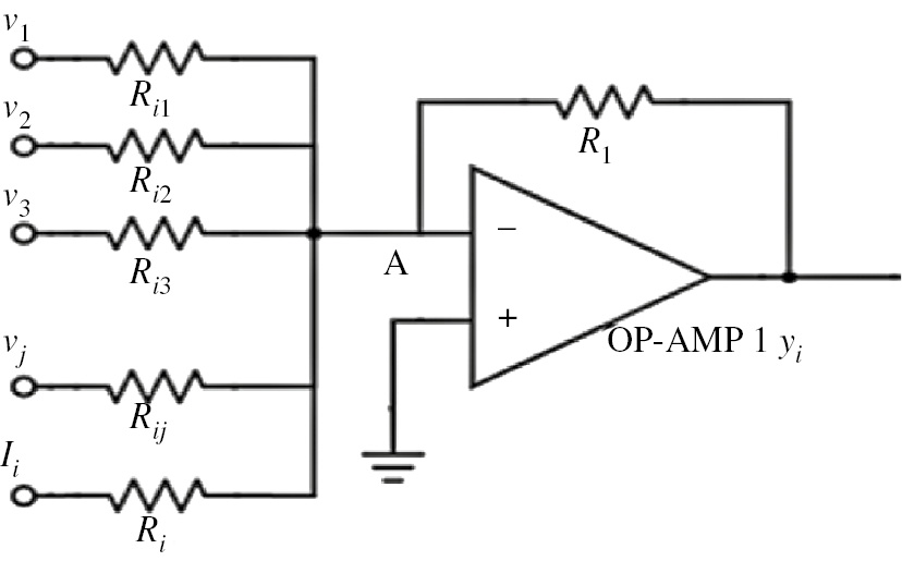
Summation circuit: v1,v2,v3,…., vj are feedbacks from other neurons, and Ii is the external input in voltage.
After applying Kirchhoff’s current law at node A and simplifying the equation, we get the following equations:
A simple inverter circuit can be used to keep output yi in phase with inputs. However, we are not using an inverter right now deliberately as we need a difference in integration circuit. This negative sign will play an important role in computing that difference. The second step is implemented using an RC circuit in the feedback path of operational amplifier, as shown in Figure 2. This circuit provides (3), which can be easily verified by simply applying Kirchoff’s current law at node B and using value of yi from (6) during the simplification of the resultant equation.
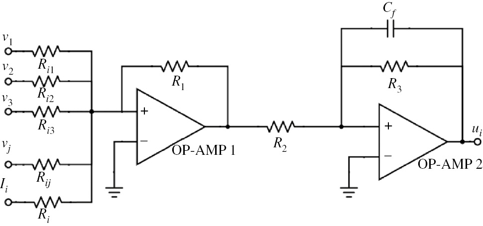
Summation circuit followed by integrator.
The circuit presented so far updates the input state of each neuron according to (3). The RC circuit presented in the integrator provides the time constant and is responsible for the settling time of the respective neuron. Irrespective of the synchronous or asynchronous mode of operation, the updating time of all neurons can be controlled through this RC value. This circuit is a full depiction of a single neuron. As it is already mentioned that neuron is analog in nature, any n-dimensional problem with an analog output can be mapped on a neural network having this neuron as a basic unit.
This analog circuit has a linear input-output relationship. If g(ui) represents an input-output relation, then
However, to design a nonlinear input-output relation or a digital output, another circuitry needs to be added. For this case, output vi is designed to be a continuous and monotonically increasing logarithmic sigmoid function of the instantaneous input ui. The following equations represent the relation for digital output:
Here K1, K2, K3, and K4 are constants and depend on circuit elements. They are designed in a way that vi remains within the [0, 1] range. The logarithmic sigmoid output is obtained through a diode pair in the feedback path of OPAMP. These diodes are connected in parallel but in opposite directions to handle ui of both signs. It binds the output range between [–VD, VD], where VD is the voltage drop across forward biased diode. Depending on the sign of ui, only one of the diodes will be in the forward bias condition. The feedback resistor R5 prevents OPAMP-3 to operate under open loop condition and to go into saturation when both diodes are off, i.e. when ui=0. In Figure 3, the circuit of OPAMP-3 provides the sigmoid output. Diode D2 is in the forward bias condition for positive values of ui, whereas diode D1 is in the forward bias state for the negative values of ui. To design the complete mathematical model of such circuit, we did a step-by-step analysis, i.e. using ui of the single polarity at a time.
![Figure 3: Logarithmic sigmoid circuit with normalized output. D1 and D2 will handle negative and positive ui, respectively. OPAMP-3 will provide sigmoid output having range [−VD, VD] range, and OPAMP-4 will normalize this sigmoid output.](/document/doi/10.1515/zna-2016-0161/asset/graphic/j_zna-2016-0161_fig_003.jpg)
Logarithmic sigmoid circuit with normalized output. D1 and D2 will handle negative and positive ui, respectively. OPAMP-3 will provide sigmoid output having range [−VD, VD] range, and OPAMP-4 will normalize this sigmoid output.
Diode D2 will go in the forward bias condition only when the value of ui is positive and voltage drop across D2 exceeds its operating voltage drop. The forward current of D2 (ID2) will remain approximately zero otherwise. As voltage drop across D2 approaches its operating voltage, the resistance of this diode decreases to a negligible level, and almost all current start flowing through it. In this case, the diode current is as follows:
where Is is the reverse bias saturation current of diode (10−12 A for silicon diode), VD is the voltage drop across diode, VT is the thermal voltage (≈26 mV at 25°C), and n is the quality factor of diode (varies between 1 and 2).
Simplifying (11),
Taking the natural logarithm of both sides and rearranging,
The same relation of ui and VD exists for the negative values of ui. However, it can be seen from Figure 3 that because of the inverting configuration, the following relation exists:
Thus,
To make vi in phase with ui and to normalize the output of each nonlinear neuron, we need a simple summation circuit. The circuit of OPAMP-4 performs both functions. However, the following two conditions must be satisfied for normalization and inversion:
1 volt is used in denominator to normalize voltage unit.
Thus,
According to (14) and (15), the constants of (8) and (9) are as follows:
Figure 4 shows the logarithmic monotonically decreasing output. It can be seen that output appears between −750 and 750 mV. The inverted and normalized output is displayed in Figure 5.
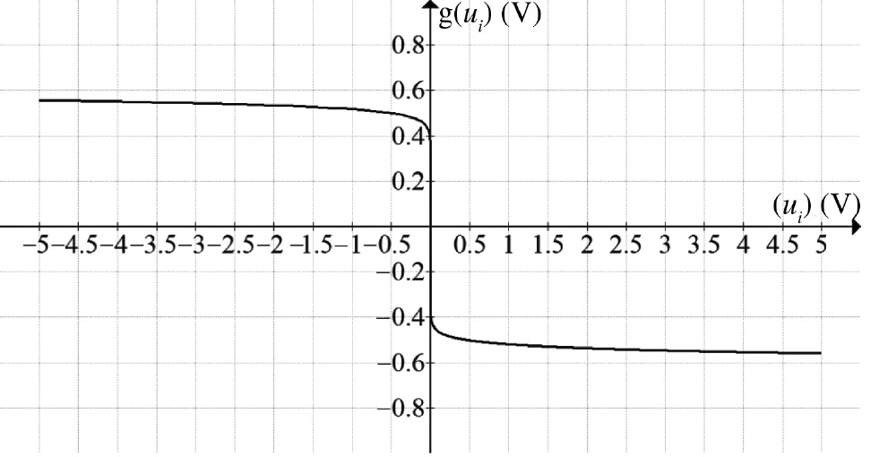
Logarithmic sigmoid monotonous decreasing output (ui versus g(ui)).
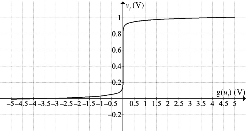
Sigmoid monotonically increasing output (g(ui) versus vi).
The complete module of a single linear neuron to mimic (2) is represented in Figure 2. The block diagram of the neuron electrical model with a linear input-output relation is represented in Figure 6a. However, for a nonlinear input-output relation, the circuit shown in Figure 3 should also be concatenated with the previous one to get the required results, as shown in Figure 6b. This circuit can be used to solve the simplest problems such as analog-to-digital converters (ADCs) as well as NP-complete problems such as travelling salesman problem, routing, etc. It can also be used in image processing, networking, database retrieval, and differential equations.
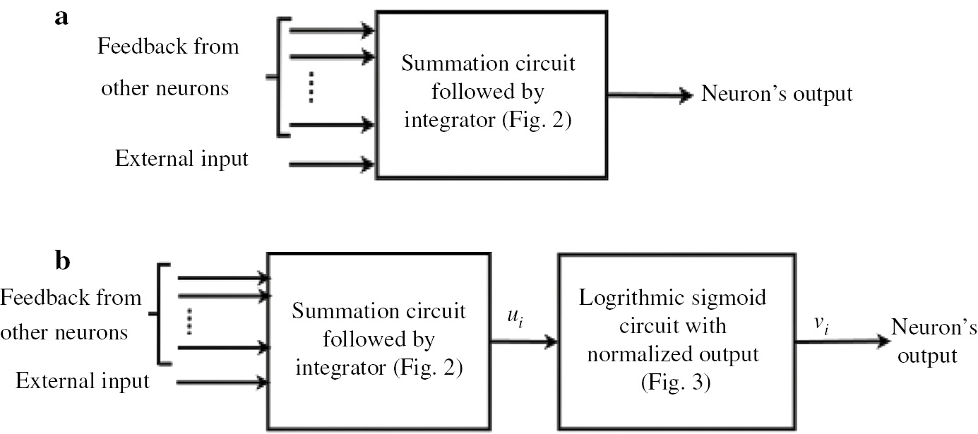
(a) Block diagram of neuron with a linear input-output relation. (b) Block diagram of neuron with a nonlinear input-output relation.
Simulation results and circuit accuracy is discussed in next section.
4 Simulation Results of Modeled Neuron
The circuit modules discussed in Section 3 can be used to solve simple as well as NP-complete optimization problems. Moreover, the selection of a neural network depicting a linear/nonlinear input-output relation depends on the problem at hand. If the output of a respective objective function is digital, then the circuit module shown in Figure 6b is used. However, the circuit of Figure 6a is considered in the case of an analog output. Dimensions of output matrix give the information about the number of neurons to be used for the solution of the problem. If we have a single output, then the single neuron is modeled. However, for one-dimensional output matrix, multiple neurons are connected in parallel fashion. For multidimensional output matrix, layers of neurons are created accordingly. None of the neurons can give feedback to itself because the matrix of feedback resistors will become positive semidefinite, which can lead to stable but oscillating results. We need a positive-definite matrix to obtain asymptotically stable results, and this matrix is obtained only by making diagonal elements zero, i.e. no self-feedback.
To verify the circuit stability and its capability to solve optimization problems, an ADC is implemented on it using an electrical module (Fig. 6b). The mapping procedure of this problem is already mentioned by Tank and Hopfield [3], [14]. According to the mapping procedure, we should design the energy function of the given problem and then map it on the components of this neural network. The energy function of this circuit is as follows:
In the case of the 4-bit ADC, the main objective function is
where a is the analog input voltage and vi is the output of each neuron. The presented circuit will be working properly if the binary combination presented by the neurons’ output becomes numerically equal to the analog input voltage [3]. The error function or cost function of (17) can be written as
If we expand and rearrange this energy function, then we will get an equation similar to (16) plus a constant value. That constant value can be disregarded without any effect on our circuit’s performance. However, it will still contain nonzero diagonal elements of the form
This term is selected to cancel the diagonal elements as well as to strengthen the optimization capability of our circuit. This term has minimum value for vi=0 as well as for vi=1. It equally favors all digital answers and will enhance the speed of achieving target. Thus, after adding (19) in (18) and rearranging terms, we get the following energy function:
The values of feedback resistors and inputs are calculated by comparing (20) with (16). Thus, the values of input bias and feedback resistances are computed from following equations:
The complete circuit for the 4-bit ADC is shown in Figure 7. The inverting output of jth neuron is connected with the input of ith neuron through resistor Rij. The inverting output is used to incorporate the negative sign in (21), and simple resistors with |1/2(i+j)| resistance are used to complete the connections. The input bias voltage and analog input a is provided through resistances |1/2(2i+1)| and |1/2i|, respectively, in terms of Ri. Again, a negative sign shown in (22) is catered by providing −1 V reference potential. Each cell has complete circuitry of a nonlinear neural network within it. The complete matrix for these resistances is given as follows:
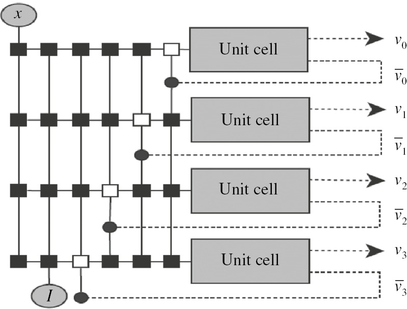
Circuit module of the 4-bit ADC. Each unit cell has a complete circuit of Figure 6b. Filled squares show feedback connections through resistor Rij, whereas filled circles represent simple wire connection. Empty squares represent open circuit.
Input bias and analog input resistors
The first term at each index in later matrix is given to the neuron with an external bias of −1 V, whereas the second term is provided with an analog input and its value can range between 0 and 15 V.
Before each simulation, initial conditions must be zero, i.e. ui=0; otherwise, this circuit does not converge properly. The values of all internally used resistances and capacitor are as follows:
Simulations are performed using a MultiSim software [National Instruments Electronics Workbench Group (formerly by Interactive Image Technologies)], and Figure 8 shows the simulation results for analog input x=9 V. Legends for each output bit are also mentioned in a standard way.
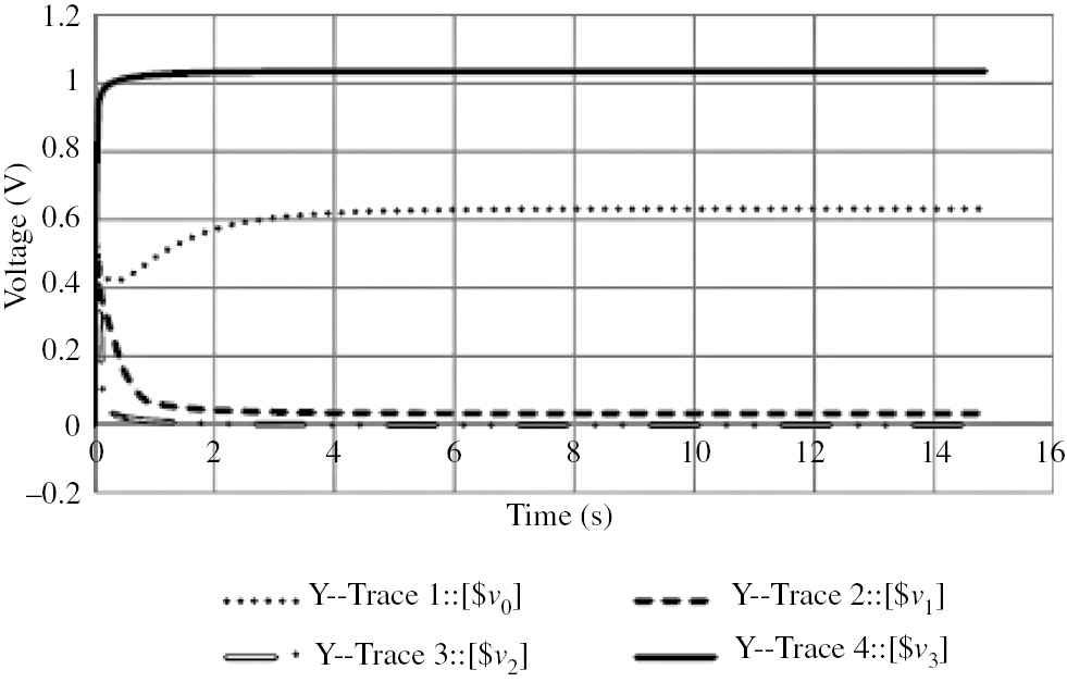
Simulation result in MultiSim for x=9 V. Output obtained was 1001. Trace 1 and trace 4 represent the least significant bit and the most significant bit, respectively.
It can be seen that the output of all cells converges to represent its 4-bit digital value. Values >0.5 V are considered as 1 V, whereas values <0.5 V are considered as 0 V. Convergence time depends on RC combination. We have simulated for different time constants, and settling time never exceeds 5∗τ under any circumstances. This circuit was checked for analog values within the 0–15 V range, and it settled down to the nearest possible digital value every time. The corresponding graph is shown in Figure 9. However, it should be kept in mind that none of the neuron or processing unit should give feedback to itself because it traps the whole system in an infinite loop and it starts oscillating between different states.
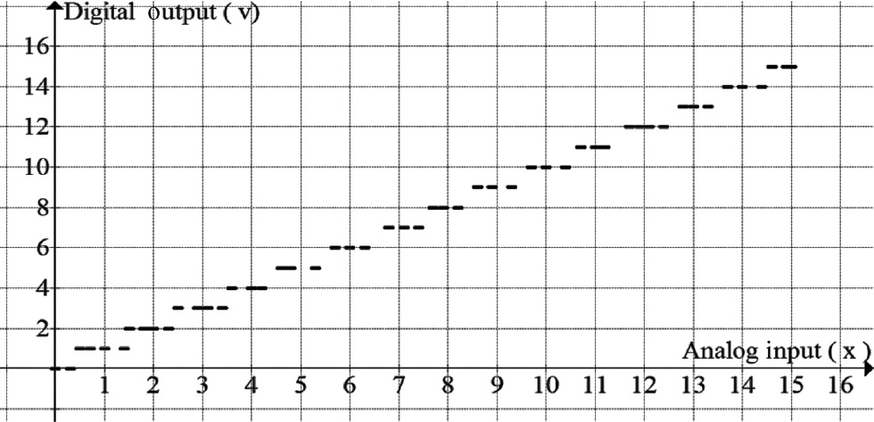
Graph of the simulation results for analog input (x) versus digital output word (v3v2v1v0).
The impulse analysis of the circuit as well as each unit cell is also stable and converges to a value quickly. A comparison of electrical models of the single neuron in terms of complexity, number of components, stability, and mapping method is summarized in Table 1. Thus far, the smallest and stable circuit of neuron was presented by Borundiya [10]. However, the mapping procedure was not discussed in his thesis, and the model has also the highest complexity level. Verleysen and Jesper [8] designed a model in 1989. This model has more electrical components than earlier presented models and their complexity level was very high. Because it was a VLSI chip, its accurate programming was therefore a difficult task. The model of Graf et al. [7] has the same problem.
Comparison of presented model with previous models.
| Models | Electrical components of the single neuron | Complexity level | Stable | Mapping method |
|---|---|---|---|---|
| Sarwar et al. (2016) (this paper) (linear model) | 2 Operational amplifiers, 1 capacitor, and 3 resistors | Low | Yes | Through energy function |
| Sarwar et al. (2016) (this paper) (nonlinear model) | 4 Operational amplifiers, 2 diodes, 1 capacitor, and 8 resistors | Low | Yes | Through energy function |
| Borundiya [10] | 8 Double gate MOSFETs, 8 resistors, 1 capacitor, and 2 zener diodes | High | Yes | Not given |
| Yamashita and Nakamura [9] | 4 Operational amplifiers, 2 diodes, 1 capacitor, and 7 resistors | Low | No | Not given |
| Verleysen and Jespers [8] | 10 MOSFETS, 1 operational amplifier, 1 XOR gate, and multiple capacitors as memory elements | High | Yes | Programmable |
| Graf et al. [7] | 6 Operational amplifiers, 4 RAM cells, 4 switches, and 2 resistors | High | Yes | Programmable |
| Hopfield and Tank [2] | 2 Analog amplifiers, 1 capacitor, and 1 resistor | Low | Yes | Through energy function |
Hopfield [2] designed a very simple model for neuron in 1984. This circuit was very simple, easy to design, and implementable. Yamashita and Nakamura’s model and our presented model are the simplest ones in terms of designing and understanding. However, Yamashita and Nakamura’s model is highly unstable, and it is not a true depiction of the Hopfield Neural Network, as claimed by them [9]. The complexity level of our presented model is low compared with all other previously presented models. Only two operational amplifiers, three resistors, and one capacitor are required for neurons with an analog output. Other electrical components are only needed to design neuron with digital output and nonlinear input-output characteristics. Stability and convergence capabilities are kept in mind in our model, and it converges to the required stability level in a fixed time irrespective of the size of complete network. MATLAB simulations (MathWorks) of resultant equations are already discussed in detail by Sarwar and Bhatti [15] and Sarwar and Iqbal [16].
5 Conclusion
A closed loop electrical circuit model is presented, which possess the properties of biological neuron. It is difficult to conceive a system in comparison with the proposed model, which will more competently solve diverse problems using a small number of neurons. This neural network model can provide analog as well as digital output and can provide accurate results in <5*τ time unit. The main objective is to accomplish an accurate mapping of the given problem over these proposed neural network models. All values can be mapped in feedback resistors and input bias voltage. The rest of the electric circuit components of each unit cell will remain the same. It is observed that the presented biological model of neurons will continue to be beneficial for simulations. Impulse response is intended and conversed to confirm the steadiness of this inventive model. A simple illustration is mapped to establish the precise exhibition of results.
References
[1] W. S. McCulloch and W. Pitts, Bull. Math. Biophys. 5, 115 (1943).10.1007/BF02478259Suche in Google Scholar
[2] J. J. Hopfield, Proc. Natl. Acad. Sci. USA 81, 3088 (1984).10.1073/pnas.81.10.3088Suche in Google Scholar PubMed PubMed Central
[3] D. Tank and J. J. Hopfield, IEEE Trans. Circuits Syst. 33, 533 (1986).10.1109/TCS.1986.1085953Suche in Google Scholar
[4] T. D. System, T. Orlowska-kowalska, S. Member, and M. Kaminski, IEEE Trans. Industr. Inform. 7, 436 (2011).10.1109/TII.2011.2158843Suche in Google Scholar
[5] S. Jain and J. D. Sharma, Int. J. Comput. Theory Eng. 2, 384 (2010).10.7763/IJCTE.2010.V2.172Suche in Google Scholar
[6] C. J. A. Bastos-Filho, R. A. Santana, D. R. C. Silva, J. F. Martins-Filho, and D. A. R. Chaves, Hopfield Neural Networks for Routing in All-Optical Networks, 2010 12th International Conference on Transparent Optical Networks, IEEE, Munich 2010, p. 1. doi: 10.1109/ICTON.2010.5549264.Suche in Google Scholar
[7] H. Graf, L. Jackel, and W. Hubbard, Computer, 21, 41 (1988).10.1109/2.30Suche in Google Scholar
[8] M. Verleysen and P. G. A. Jespers, IEEE Micro, 9, 46 (1989).10.1109/40.42986Suche in Google Scholar
[9] Y. Yamashita and Y. Nakamura, A Neuron Circuit Model with Smooth Nonlinear Output Function, 2007 International Symposium on Nonlinear Theory and its Applications, NOLTA’07, Vancouver, Canada 2007, p. 11.Suche in Google Scholar
[10] A. P. Borundiya, Implementation of Hopfield Neural Network Using Double Gate MOSFET, Ohio University, Athens, Ohio, USA 2008.Suche in Google Scholar
[11] N. D. Patel, S. K. Nguang, and G. G. Coghill, IEEE Trans. Neural Netw, 18, 1488 (2007).10.1109/TNN.2007.895822Suche in Google Scholar PubMed
[12] S. Himavathi, D. Anitha, and A. Muthuramalingam, IEEE Trans. Neural Netw, 18, 880 (2007).10.1109/TNN.2007.891626Suche in Google Scholar PubMed
[13] H. Asgari and Y. S. Kavian, Neural Netw. World, 2, 211 (2014).10.14311/NNW.2014.24.013Suche in Google Scholar
[14] J. J. Hopfield and D. W. Tank, Biol. Cybern. 52, 141 (1985).10.1007/BF00339943Suche in Google Scholar PubMed
[15] F. Sarwar and A. A. Bhatti, Critical Analysis of Hopfield’s Neural Network<Model and Heuristic Algorithm for Shortest Path Computation for Routing in Computer Networks, Applied Sciences and Technology (IBCAST), 2012 9th International Bhurban, 2012, p. 115.10.1109/IBCAST.2012.6177539Suche in Google Scholar
[16] F. Sarwar and S. Iqbal, Z. Naturforsch. A, 69, 129 (2014).10.5560/zna.2013-0082Suche in Google Scholar
©2016 Walter de Gruyter GmbH, Berlin/Boston
Artikel in diesem Heft
- Frontmatter
- Studying of the Nucleus-Nucleus Interaction Using Wave Function of the Nucleus and Hyperspherical Formalism
- Highly Accurate Compact Difference Scheme for SPL Heat Conduction Model of General Body
- Linear and Nonlinear Electrical Models of Neurons for Hopfield Neural Network
- Flow and Heat Transfer of Bingham Plastic Fluid over a Rotating Disk with Variable Thickness
- Boriding of Binary Ni–Ti Shape Memory Alloys
- The Wheeler–DeWitt Equation in Filćhenkov Model: The Lie Algebraic Approach
- Quasi-Exact Solutions for Generalised Interquark Interactions in a Two-Body Semi-Relativistic Framework
- Multi-Scale Morphological Analysis of Conductance Signals in Vertical Upward Gas–Liquid Two-Phase Flow
- Exact Solutions for a Coupled Korteweg–de Vries System
- Symmetry Reductions and Exact Solutions to the Kudryashov–Sinelshchikov Equation
- Improving Charge Transport in PbS Quantum Dot to Al:ZnO Layer by Changing the Size of Quantum Dots in Hybrid Solar Cells
- Calculation of Liquid–Solid Interfacial Free Energy in Pb–Cu Binary Immiscible System