First-Principle Study of the Structural, Electronic, and Optical Properties of Cubic InNxP1–x Ternary Alloys under Hydrostatic Pressure
-
I. Hattabi
 ,
R. Moussa
,
R. Moussa

Abstract
In this article, we present results of the first-principle study of the structural, electronic, and optical properties of the InN, InP binary compounds and their related ternary alloy InNxP1–x in the zinc-blend (ZB) phase within a nonrelativistic full potential linearised augmented plan wave (FP-LAPW) method using Wien2k code based on the density functional theory (DFT). Different approximations of exchange–correlation energy were used for the calculation of the lattice constant, bulk modulus, and first-order pressure derivative of the bulk modulus. Whereas the lattice constant decreases with increasing nitride composition x. Our results present a good agreement with theoretical and experimental data. The electronic band structures calculated using Tran-Blaha-modified Becke–Johnson (TB-mBJ) approach present a direct band gap semiconductor character for InNxP1–x compounds at different x values. The electronic properties were also calculated under hydrostatic pressure for (P=0.00, 5.00, 10.0, 15.0, 20.0, 25.0 GPa) where it is found that the InP compound change from direct to indirect band gap at the pressure P≥7.80 GPa. Furthermore, the pressure effect on the dielectric function and the refractive index was carried out. Results obtained in our calculations present a good agreement with available theoretical reports and experimental data.
1 Introduction
Semiconductor compounds are the basis materials for different fields of technologies, as well as new classes of optoelectronic devices. Some examples include high electron mobility and transistors, heterostructures, light-emitting diodes, photodetectors, and modulators.
The InN and InP compounds are interesting semiconductors materials for high-frequency electronic devices, by reason of its superior speed electrons. These alloys have undergone a variety of experimental and theoretical studies. Recently, in experimental study, the electronic structure of InP was studied by Ley et al. [1]. Aspnes and Studna measured the dielectric function of III–V semiconductors of InP and obtained more other optical constants in the energy range 1.5–6.0 eV [2]. Besides, the dielectric constants of InP compound between 0.7 and 5.0 eV including a band gap around 1.42 eV measured by Herzinger et al. [3]. The direct band gap of high-quality wurtzite InN films is reported [4, 5] to be from 0.65 to 1 eV. The band gap of the cubic InN is foreseen to be within this range or slightly lower. This allows manufacturing the high-speed LDs and PDs for optical communication systems [4]. On the other hand, some results for structural and electronic properties were reported by Boussahla et al. [6], as well as Ben Fredj et al. [7, 8]. The strong dependence of the band gap on the N content has made diluted III–V nitrides important materials for a variety of applications, including long wavelength optoelectronic devices [9, 10] and high-efficiency hybrid solar cells [11, 12]. Several theoretical studies of band structure calculations using density functional theory (DFT) have addressed the unusually strong dependence of the fundamental gap on the N content in the group III–N–V alloys [13, 14]. Recently, structural and electronic properties of InNxP1–x alloys were investigated in full range (0<x<1) by Aslan et al. [15].
Some of the III–V compounds, in particular the InP, InN, and their ternary InNxP1–x solid solutions form crystals with zinc blende arrangement, which is based on the cubic space group F4̅3m in which the lattice parameter obeys to the Vegard’s law and varies linearly with the composition x of nitrogen [16].
Here, we investigate the structural, electronic, and optical properties of the cubic InN and InP binary compounds together with their related ternary InNxP1–x solid solutions using the first-principles calculations by performing the Tran–Blaha-modified, Becke–Johnson (TB-mBJ) approach band structure calculations. The electronic and optical properties were also carried out under hydrostatic pressure effect. The calculations were made by applying a nonrelativistic full potential linearised augmented plane waves (FP-LAPW) method in the context of the DFT as implemented in the Wien2k package [17].
2 Computational Details
Calculations were performed using DFT because of the efficiency of this approach for different systems. For periodic systems, we have gathered an extensive experience with the all-electron full-potential linearised plane wave (FP-LAPW)-based code Wien2k [18]. This code uses “forces” to optimise the crystal structure. The periodical calculations of properties, at the k-space through the Fourier transformations techniques, employed in expansions of both the electronic wave functions and the potential generated by the nucleus.
The exchange–correlation potential was treated within the generalised gradient approximation (WC-GGA). In addition to this approximation, the (local density approximation, LDA) and (PBE-sol GGA) was also applied for computing structural properties such as the lattice constants, bulk modulus, and their pressure derivatives. The obtained results were fitted using the Birch–Murnaghan’s equation of state [19].
In order to model the InNxP1–x alloys with different compositions x=0.0, 0.25, 0.5, 0.75, and 1.0, we have used a cubic cell 1×1×1 with eight atoms. For each configuration, the band gap energy, the dielectric constants, and the refractive index were studied under hydrostatic pressure effect for different values of pressure (P=0, 5, 10, 15, 20, 25 GPa). The matrix size was defined with a parameter Rmt×Kmax equal to 8, where the Rmt denotes the minimum radius of the sphere in unit cell, and Kmax yields the extent of the largest K vector in the plane wave expansion. The muffin-tin radii of In, N, and P are adopted to be 2.1, 1.4, and 1.7 Bohr, respectively. We have chosen a value of –6.0 Ry for the energy cutoff between the core and the valence states for both compounds, we have fixed lmax=10 for wave function expansion inside the atomic spheres and the charge density was Fourier expanded up to Gmax=12 (Ryd). The integrals over the Brillouin zone are performed up to 47 k-points, the energy convergence was selected as 0.0001 Ry.
The band structures were calculated using the TB-mBJ approach with the parameterisation of Koller et al. [20]. The total and partial densities of states (DOSs) were calculated. We have to note that for the DOS calculations, we have used a denser k-mesh of 3000 k-points and we have distinguished the In (1s2 2s2 2p6 3s2 3p6 3d10 4s2 4p6), N (1s2), and P (1s2 2s2 2p6) as inner-shell electrons from the valence electrons of In (4d10 5s2 5p1), N (2s2 2p3), and P (3s2 3p3) shells.
3 Results and Discussion
3.1 Structural Properties
The lattice constants (a), bulk modulus (B), and pressure derivatives of the bulk modulus (B′) at the corresponding volumes of cubic InNxP1–x alloys using the LDA, WC-GGA, and PBEsol-GGA approximations, for different compositions (x=0.00, 0.25, 0.50, 0.75, 1.00), are computed. Results obtained are summarised in Table 1, together with available measured values and other theoretical available data. Our calculated lattice constants are very close to those given in the literature. We show as a prototype in Figure 1 the variation of total energy as a function of volume by fitting the total energies to the Murnaghan’s equation of state [19].
The lattice constants (a), bulk modulus (B), and pressure derivative of the bulk modulus (B′) for the InN, InP, and the zinc blende InNx P1–x alloys.
| Composition x | Parameters | This work | Other theoretical studies | Experimental data | ||
|---|---|---|---|---|---|---|
| WC-GGA | PBEsol-GGA | PW-LDA | ||||
| InN | a (Å) | 4.9926 | 4.9918 | 4.9471 | 4.945a, 4.98b | 4.98f |
| B (GPa) | 140.5343 | 137.2588 | 145.5469 | 145a, 155.35b | 137e | |
| B′ | 4.1757 | 3.7960 | 3.6884 | 4.75c, 4.49b | ||
| InN0.75P0.25 | a (Å) | 5.2638 | 5.2624 | 5.2131 | ||
| B (GPa) | 103.3437 | 103.0356 | 111.7882 | |||
| B′ | 4.7490 | 4.3744 | 4.7623 | |||
| InN0.5P0.5 | a (Å) | 5.5052 | 5.5036 | 5.4525 | ||
| B (GPa) | 84.1868 | 83.7418 | 92.0391 | |||
| B′ | 4.5969 | 4.1304 | 4.3859 | |||
| InN0.25P0.75 | a (Å) | 5.7105 | 5.7087 | 5.6579 | ||
| B (GPa) | 73.0259 | 72.8655 | 78.5801 | |||
| B′ | 4.3392 | 4.5467 | 4.6981 | |||
| InP | a (Å) | 5.8814 | 5.8789 | 5.8299 | 5.72d, 5.85g | 5.86d |
| B (GPa) | 67.7383 | 67.2997 | 71.0719 | 73.66d, 76.10h | 72.00d | |
| B′ | 4.3041 | 4.5021 | 4.6221 | 4.20i | 4.80i | |
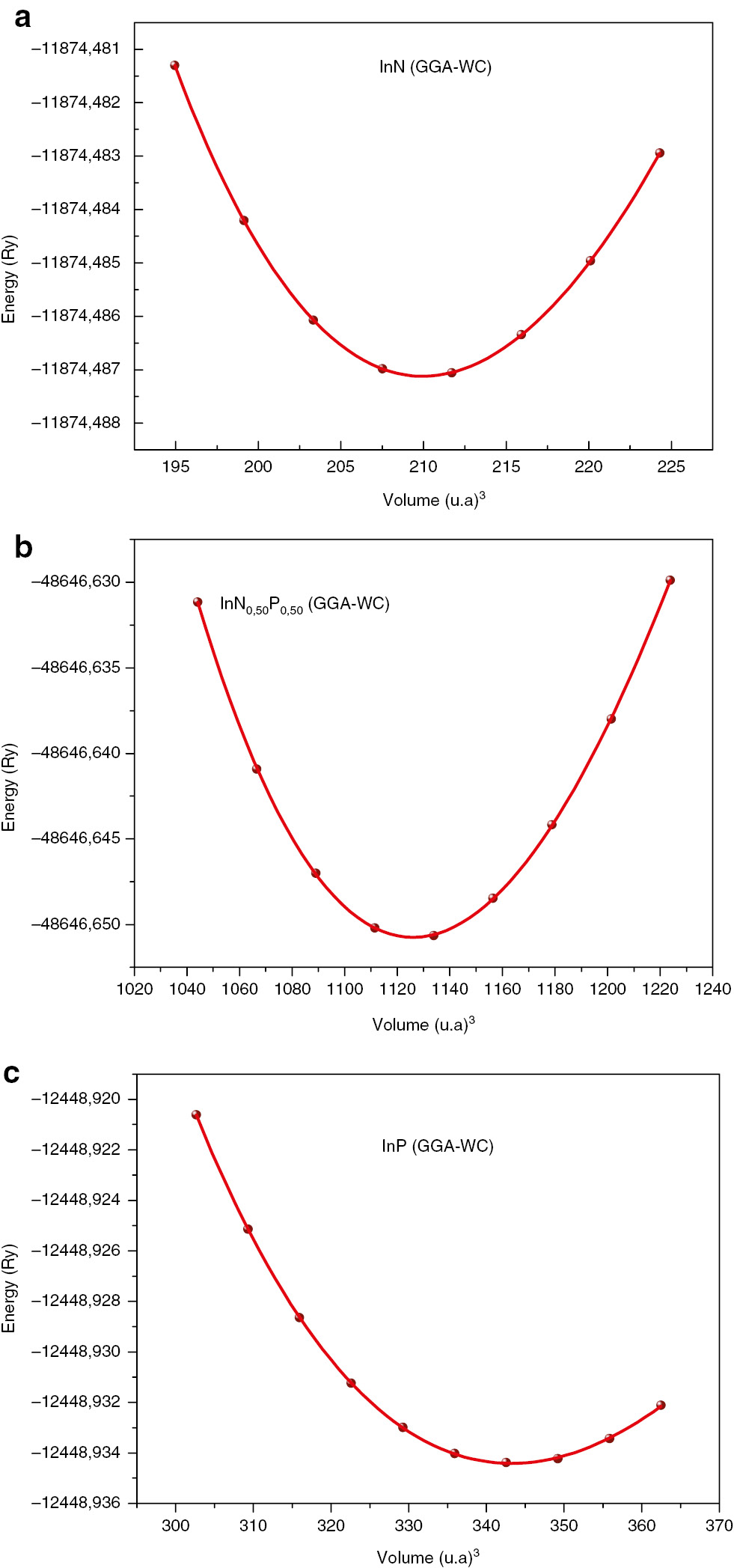
Energy versus volume curves of (a) InN, (c) InP, and (b) InN0.5P0.5 compounds for WC-GGA exchange–correlation energy approximations.
The difference can be observed between the lattice parameter value of InP (x=0, a0=5.88 Å) compound, and these of the InN (x=1, a0=4.99 Å) can be explained by the difference in the atomic radius of the P (0.98 Å) atom from that of the atom N (0.65 Å), which allows us to note that the decrease in lattice parameter of the InNxP1–x ternary compounds have an inversely relationship with increasing x composition. In opposition to the lattice constant a0 and in concordance with the proportionality between the Bulk modulus and the lattice constants:
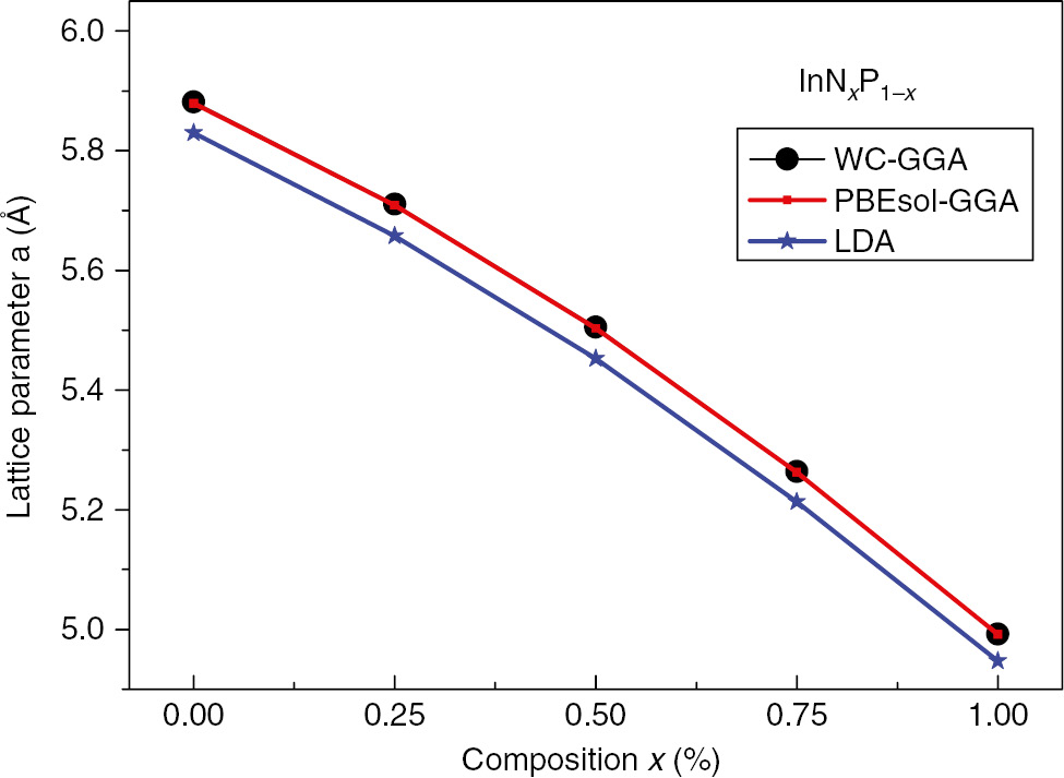
Variation of the lattice constant versus composition, x, of the (ZB) InNxP1–x alloy.
The bowing parameters of the lattice constants curves are found to be equal to –0.27051, –0.27074, and –0.25371 for the WC-GGA, PBEsol-GGA, and PW-LDAs, respectively.
With the same scheme, we have calculated the bowing parameter of the bulk modulus for InNxP1–x, solid solutions. Values are 82.0594, 75.1226, and 67.1898 for the WC-GGA, PBEsol-GGA, and PW-LDA approaches, respectively. The bulk modulus versus composition x for the InNxP1–x alloys are depicted in Figure 3. Unfortunately, we have not found any report in literature for more comparison of our results for the ternary alloys InNxP1–x.
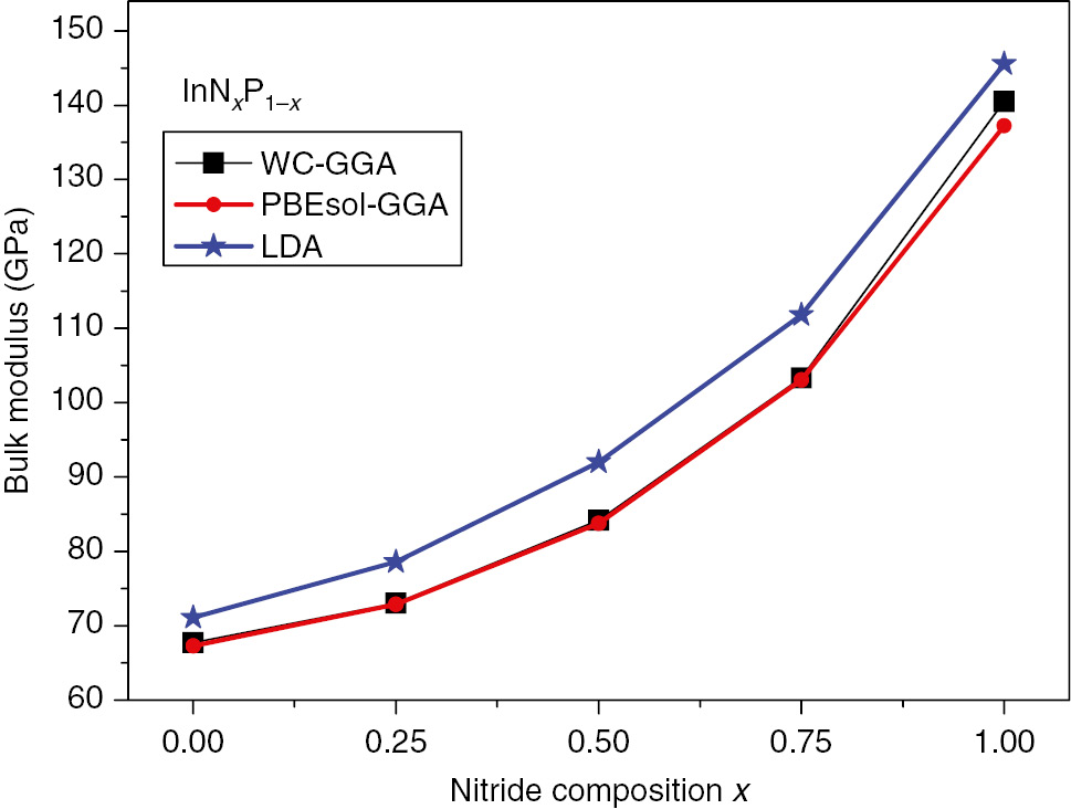
Variation of the bulk modulus versus composition, x, of the (ZB) InNxP1–x alloy.
3.2 Electronic Structure
In this section, the energy band structures and the density of states DOS are investigated for both binary constituents InP, InN, and their related ternary alloys InNxP1–x. For a wide range of materials, standard DFT calculations using modern approximations as well as the generalised gradient approach (GGA), the local density LDA, and other approximations give extremely useful results in structural properties calculations, but it is known that they underestimate dramatically the band gaps of most semiconductors and leads to incorrect prediction comparing with experimental results. In this regard, we have introduced the Tran–Blaha-modified Becke Johnson (TB-mBJ) approach in our calculations. The TB-mBJ approximation gives a very much improved band gaps for a large variety of materials including semiconductors.
In this approach, the TB-mBJ potential is given by
where c is given by
where g′ is the average of g=|∇ρ|/ρ in the unit cell of volume Vcell. According to a fit to the experimental values of band gaps, A and B parameters values are A=–0.012 and B=1.023 bohr1/2.
Results obtained using this approach are closed to the available experimental data. The calculated band structures of the InNxP1–x compounds at different composition x=(0.00, 0.25, 0.50, 0.75, 1.00), within the TB-mBJ approximation, are shown in Figure 4.
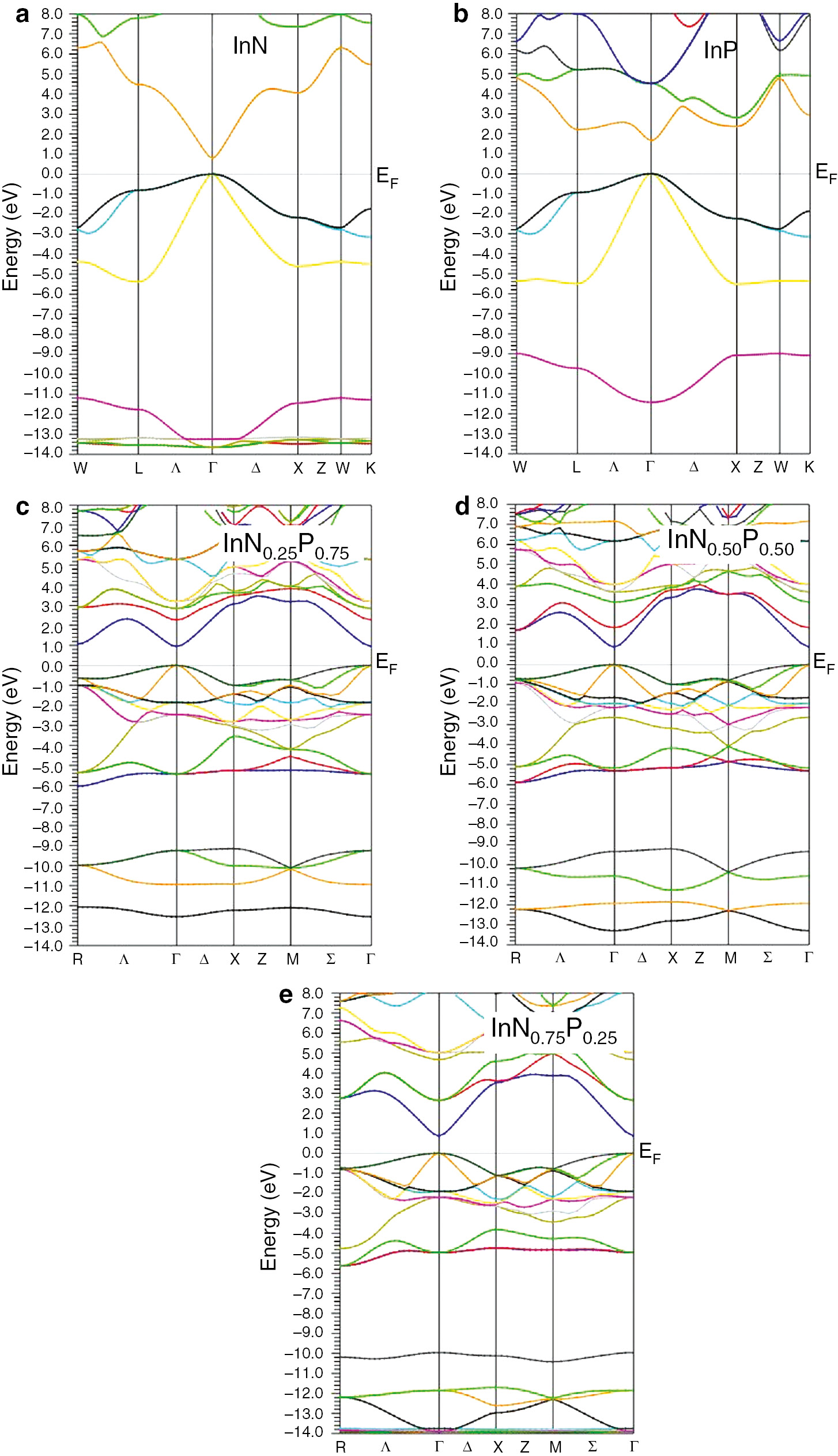
(a, b) The electronic band structures of the cubic (a) InN and (b) InP alloys within TB-mBJ approximation. The electronic band structures of the cubic (c) InN0.25P0.75, (d) InN0.5P0.5 and (e) InN0.75P0.25 alloys within TB-mBJ approximation.
Our calculations allow us to notice that the considered compounds are semiconductors in the range of all concentrations with a direct band gap of about 0.79, 0.87, and 1.66 eV, for the InN, InN0.5P0.5, and InP, respectively. These values confirm the importance of these compounds for the design and analysis of various optoelectronic and photonic devices.
Results obtained here for the direct band gap (Γ→Γ) and indirect one (Γ→X), for each concentration x, are reported in Table 2. It is clearly seen that the InNxP1–x direct band gap (EΓ→Γ) increases when composition x decreases and can be explained by the effect of N-dopant on the decrease in lattice parameter and also the presence of new energy bands in the material. Inversely, the indirect (EΓ→X) band gap decreases with the P-dopant augmentation.
The band gap energies of the direct and indirect transitions of the InNx P1–x compounds for the compositions (x=0.00, 0.25, 0.50, 0.75, and 1.00), where the values are given in electron volts.
| Composition x at P atom | Band gap energy (eV) | This work | Other theoretical studies | Experimental data |
|---|---|---|---|---|
| LDA_mBJ | ||||
| InN | EΓ→Γ | 0.79110 | 0:69a | 0.7b |
| EΓ→X | 4.06859 | 2.765c | 2:11d | |
| InN0.75P0.25 | EΓ→Γ | 0.86179 | ||
| EΓ→X | 3.52952 | |||
| InN0.5P0.5 | EΓ→Γ | 0.87223 | ||
| EΓ→X | 3.35265 | |||
| InN0.25P0.75 | EΓ→Γ | 0.94014 | ||
| EΓ→X | 3.07013 | |||
| InP | EΓ→Γ | 1.66753 | 1.423e | 1.35f |
| EΓ→X | 2.36479 | 1.63g | 2.21f |
Moreover, the variation curves versus composition x of each band gap (EΓ→Γ, EΓ→X) undergo a simple polynomial quadratic fit and are shown in Figure 5. The InNxP1–x bowing factor values of the energy gap is found to be 1.5625 and –0.5007 eV for direct and indirect transitions, respectively.
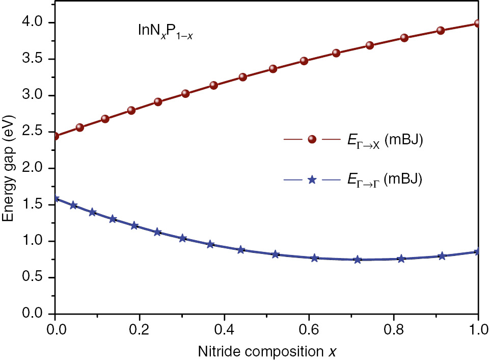
The variations curves versus composition x of each band gap (EΓ→Γ, EΓ→X) of the InNxP1–x alloys.
The equations of fitted curves of the InNxP1–x direct and indirect band gaps are given by the following equations:
3.3 Density of States
The density of states tells us how many states per unit energy exist in the vicinity of a certain energy level.
Figure 6 shows the total and the partial densities of states of InN, InP, and InN0.5P0.5 alloys, respectively. They were calculated using the plane wave-local density approximation (PW-LDA). It can be seen from Figure 6a that the valence band comprises two regions, a lower (LVB) and upper (UVB) bands, respectively. For the InN compound, the In-4d and N-2s states are dominant in the LVB, with a high contribution of In-4d states, while the UVB is dominated by In-5s states, with a little contribution of In-5p and N-2s states. The conduction band (CB) is essentially populated by In-5s, In-5p and N-2p states.
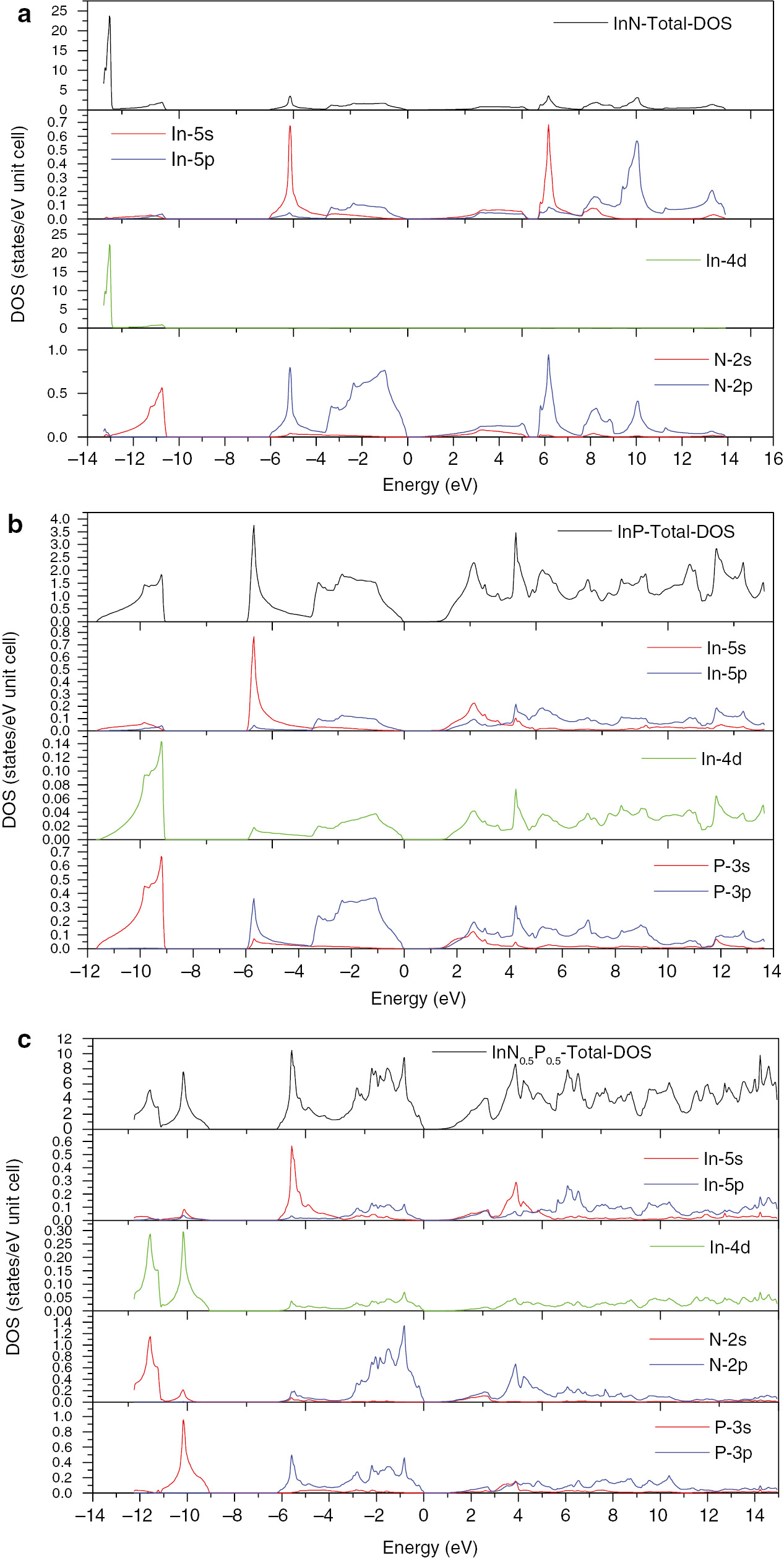
The total and partial density of states for the (a) InN, (b) InP, and (c) InN0.5P0.5 alloys.
It is seen from Figure 6b that the In-4d and P-3s orbital contribute to the UVB of the DOS in InP binary compound. The uppermost part of the valence band is dominated of the In-5p and P-3p states, with a small contribution of In-4d states. The CB is formed of a mixture of all states, with a high contributions of the In-5s and P-3p orbitals.
It is observed from Figure 6c that in the InN0.50P0.50 ternary alloy, the LVB is mainly populated by In-4d, N-2s and P-3s states. The UVB is essentially formed by In-5s and a mixture of In-5p, N-2p and P-3p states. The CB results from a mixture of In-5s, In-5p, and a small contribution of N-2p and P-3p states.
4 Optical Properties
In order to investigate the optical properties of the ternary alloys InNxP1–x, we have studied all the possible transitions between valence and CBs. The frequency-dependent dielectric functions ε1(ω) and ε2(ω) [34], the real and imaginary parts of the complex dielectric function ε(ω) are given by the following equations:
In the imaginary part ε2(ω), the momentum dipole elements
describes the direct transitions between the valence band and the CB uvk and uck states, respectively, with δ as a unit vector defining the electric field. The integral is carried out over the first Brillouin zone.
On the other hand, P designates that the integral is to be evaluated in the principal value sense in the real part ε1(ω). This latter can be calculated from imaginary part by means of the Kramers–Kronig transformation [35].
The spectral variations of the dielectric function ε(ω) within the real and imaginary parts for the InN, InP compounds, and their related ternary InNxP1–x alloy at the composition x=0.5 are shown in Figure 7.
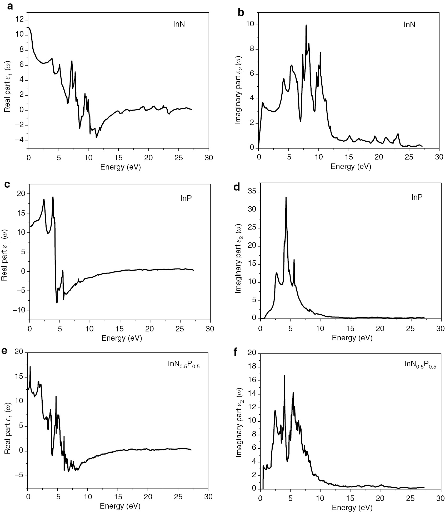
The real and imaginary parts of the dielectric function of the (ZB) (a, b) InN, (c, d) InP, and (e, f) InN0.5P0.5 alloys.
From the variation curves of the imaginary part of the dielectric function ε2(ω) according to the energy, which reflects the absorption of the material. We can get different direct interband transitions. The main peaks of the structure are visible at 3.70, 5.63, 7.6, and 9.98 eV which correspond well to the InN compound at energies 0.72, 4.20, 7.33, 7.93 eV, respectively. These peaks may belong to the electronic direct transition from In-3p states to In-4s and N-2p states as predicted by Usman et al. [36]. The peak around 7.33 eV is attributed to 3p, 4s valence states of Indium to N-2p and In-4s [36]. Whereas, the peak at 9.98 eV is related to mixed transitions.
For the InP alloy, we observe two peaks located at 2.73 and 4.23 eV. We have to note that our calculated peak positions are much closer to Feng et al. data (3.06, 4.69 eV) [37] than the calculated values (2.40, 4.10 eV) [38] using the FPLMTO method. The first peak corresponds mainly to the interband direct transitions from the top of valence bands to the bottom of CBs.
The maximum of absorption is located at 9.98, 33.55, and 16.76 eV for InN, InP, and InN0.5P0.5, respectively.
Moreover, we have calculated the refractive index n(ω) using the following relation:
Other models were used to calculate the refractive index n(ω) for comparison and confirmation of results. These models are presented as follow:
Moss model [39]:
where n and Eg are, respectively, the refractive index and the energy gap.
Ravindra model [39]:
Herve–Vandamme model [39]:
where A is the hydrogen ionisation energy 13.6 eV and B=3.47 eV is a constant presumed to be the difference between the UV resonance energy and the band gap Eg.
Reddy model [39]:
Kumar and Singh model [39]:
where K=3.3668 and C=–0.32234.
The static values of the refractive index n(ω) for ω=0 are listed in Table 3. As can be seen from Figure 10, the refractive index n(ω) decreases when increasing the nitrogen composition x. The values obtained here are also computed using different models (8–12), cited above, for the validation and comparison purposes. Results agree well between these models.
The refractive index n of the InNxP1–x compounds (x=0.00, 0.50, 1.00).
| Compound | FP-LAPW n(ω=0) | Herve–Vandam n(ω=0) | Ravindran n(ω=0) | Reddy n(ω=0) | Moss n(ω=0) | Kumarn (ω=0) | Other works n(ω=0) |
|---|---|---|---|---|---|---|---|
| InN | 3.32 | 3.39 | 3.59 | 3.83 | 3.31 | 3.63 | 2.92a |
| InN0.5P0.5 | 3.52 | 3.34 | 3.55 | 3.74 | 3.24 | 3.53 | – |
| InP | 3.39 | 2.86 | 3.15 | 3.08 | 2.75 | 2.85 | 3.32b |
5 Hydrostatic Pressure Effect
When a material is destined for a technological application, it becomes necessary to study the comportment of the material under external disturbances such as pressure, temperature, electric field, and magnetic field. In this article, we have chosen to study the hydrostatic pressure on the energy gaps and the optical properties.
Variations of band gap energies and optical properties under hydrostatic pressure were calculated using the FP-LAPW methods within LDA and TB-mBJ approach, respectively. Firstly, we have calculated the lattice constant values as a function of pressure at P equal to 0, 5, 10, 15, 20, and 25 GPa, using the following formula [42]:
where B is the bulk modulus, B′ the pressure derivative of the bulk modulus, and a(P) the lattice parameter at the indicated pressure P.
The direct and indirect band gap energies of the InNxP1–x at x=0.00, 0.50, and 1.00 compositions were computed and plotted in Figure 8.
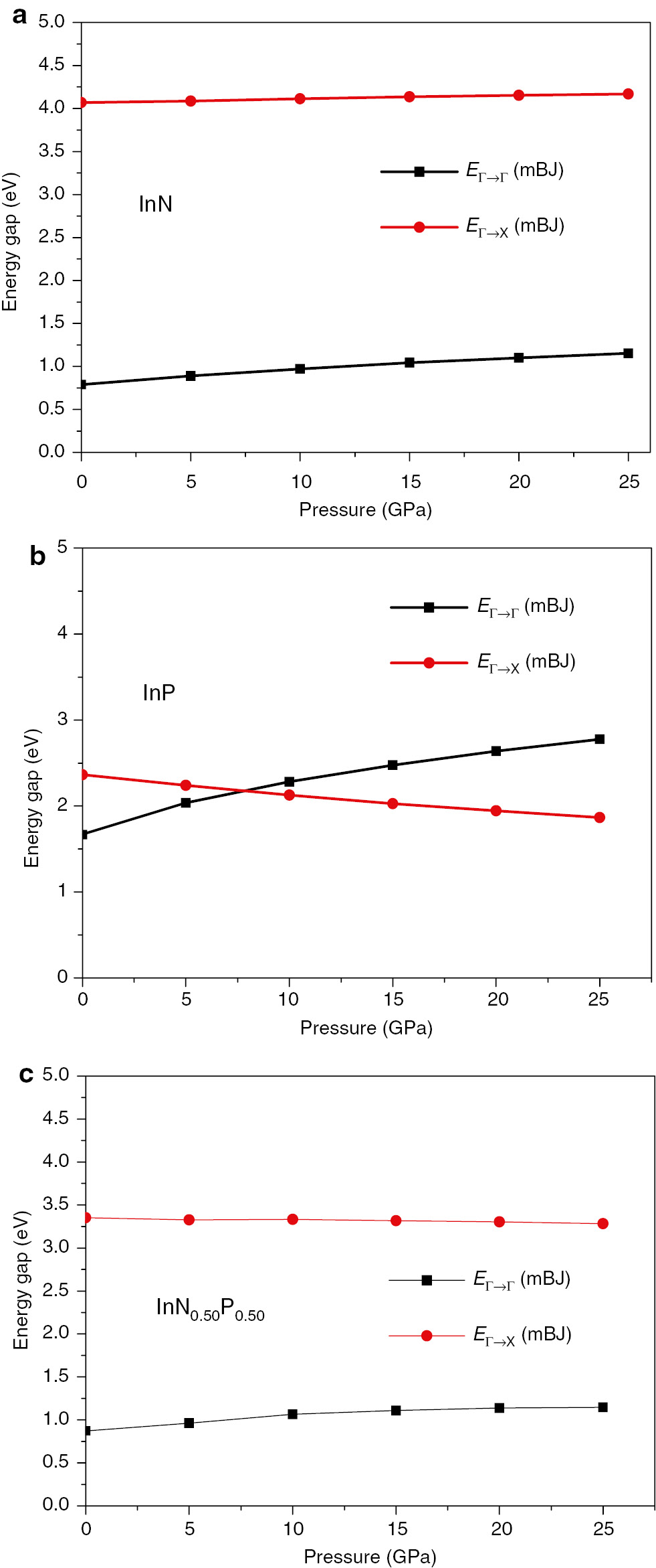
The direct and indirect band gaps energies versus pressure of (a) InN, (b) InP, and (c) InN0.5P0.5 alloys.
When the applied pressure is increased, a small variation for both gap energies is observed with an increase in the direct band gap EΓ→Γ and a decrease in the indirect band gap EΓ→X, and that is due to the decrease of the lattice constant (volume compression). We can also notice that the InP compound changes character from a direct to an indirect band gap semiconductor at P≥7.80 GPa. The direct and indirect band gap energy values are listed in Table 4. Furthermore, we have fitted our results to a quadratic function as given in the empirical formula [42]:
The direct and indirect gap energies of the InN, InP, and InN0.50P0.50 compounds at different pressure values with TR-mBJ approach.
| Composition x at P atom | Band gap energy (eV) | Hydrostatic pressure P (GPa) | |||||
|---|---|---|---|---|---|---|---|
| 0 | 5 | 10 | 15 | 20 | 25 | ||
| InN | EΓ→Γ | 0.79110 | 0.88842 | 0.97088 | 1.04396 | 1.10098 | 1.15155 |
| EΓ→X | 4.06859 | 4.08692 | 4.11275 | 4.13811 | 4.15406 | 4.17004 | |
| InN0.75P0.25 | EΓ→Γ | 0.86179 | 0.98163 | 1.07573 | 1.15816 | 1.22139 | 1.27984 |
| EΓ→X | 3.52952 | 3.61036 | 3.67263 | 3.72586 | 3.76517 | 3.80134 | |
| InN0.5P0.5 | EΓ→Γ | 0.87223 | 0.96123 | 1.06396 | 1.10902 | 1.13676 | 1.14807 |
| EΓ→X | 3.35265 | 3.32565 | 3.33382 | 3.31844 | 3.30200 | 3.28279 | |
| InN0.25P0.75 | EΓ→Γ | 0.94014 | 0.98412 | 0.97020 | 0.92748 | 0.87693 | 0.82095 |
| EΓ→X | 3.07013 | 3.02893 | 2.98615 | 2.94030 | 2.89729 | 2.85431 | |
| InP | EΓ→Γ | 1.66753 | 2.03754 | 2.28303 | 2.47566 | 2.63950 | 2.77618 |
| EΓ→X | 2.36479 | 2.24213 | 2.12825 | 2.02815 | 1.94413 | 1.86804 | |
where Eg(0) represents the band gap energy at zero pressure, P is the pressure in GPa, α and β are the first- and second-order pressure coefficients, respectively. The pressure coefficients α and β obtained from the fitted curves of the cubic InN and InP binary compounds as well as the InN0.50P0.50 ternary alloy are summarised in Table 5. Results obtained here are compared to the available data where a good agreement is observed for binary constituents. We have to note that we have not found any report in literature for comparison.
The hydrostatic pressure coefficients, α and β for the cubic InN, InP, and InN0.50P0.50 compounds.
| Compounds | Band gap (TB-mBJ) | α (10−2 eV/GPa) | B (10−4 eV/GPa) |
|---|---|---|---|
| InN | EΓ→Γ | 2.03, 2.54a | –2.39, –1.51a |
| EΓ→X | 0.51, 0.59a | –0.36, –0.53a | |
| InN0.50P0.50 | EΓ→Γ | 2.34 | –4.91 |
| EΓ→X | –0.14 | –0.42 | |
| InP | EΓ→Γ | 6.97, 7.81a | –10.7, –10.53a |
| EΓ→X | –2.61, –2.09a | 2.51, 1.65a |
aRef. [43].
We reported on the optical properties under different values of pressure for InN, InP, and InN0.50P0.50 alloys. The dielectric functions versus photon energy and the behaviour of refractive indices at various hydrostatic pressures were investigated and shown in Figures 9 and 10, respectively. We can see the similarity of spectra of the dielectric function under different values of pressure except of a slight shift explained by the effect of pressure on the band energies. On the other hand, the refractive index decreases slightly due to the condensation of atoms and compression of the unit cell volume. It is clearly seen from Figure 10a–c that the refractive index decreases dramatically versus pressures for the InN compound. For the second binary compound InP, we observe a decrease in the value of the refractive index versus pressure. The maximum of the value of the refractive index is found to be equal to 5.4 and observed at the energy value of 4.85 eV. The refractive index of the ternary alloy InN0.50P0.50 obeys to the same behaviour and the maximum of the refractive index is 4.24 and it is located at the energy value of 0.5 eV. Roughly, the pressure presents no significant effect and this confirms the stability of optical properties of our material.
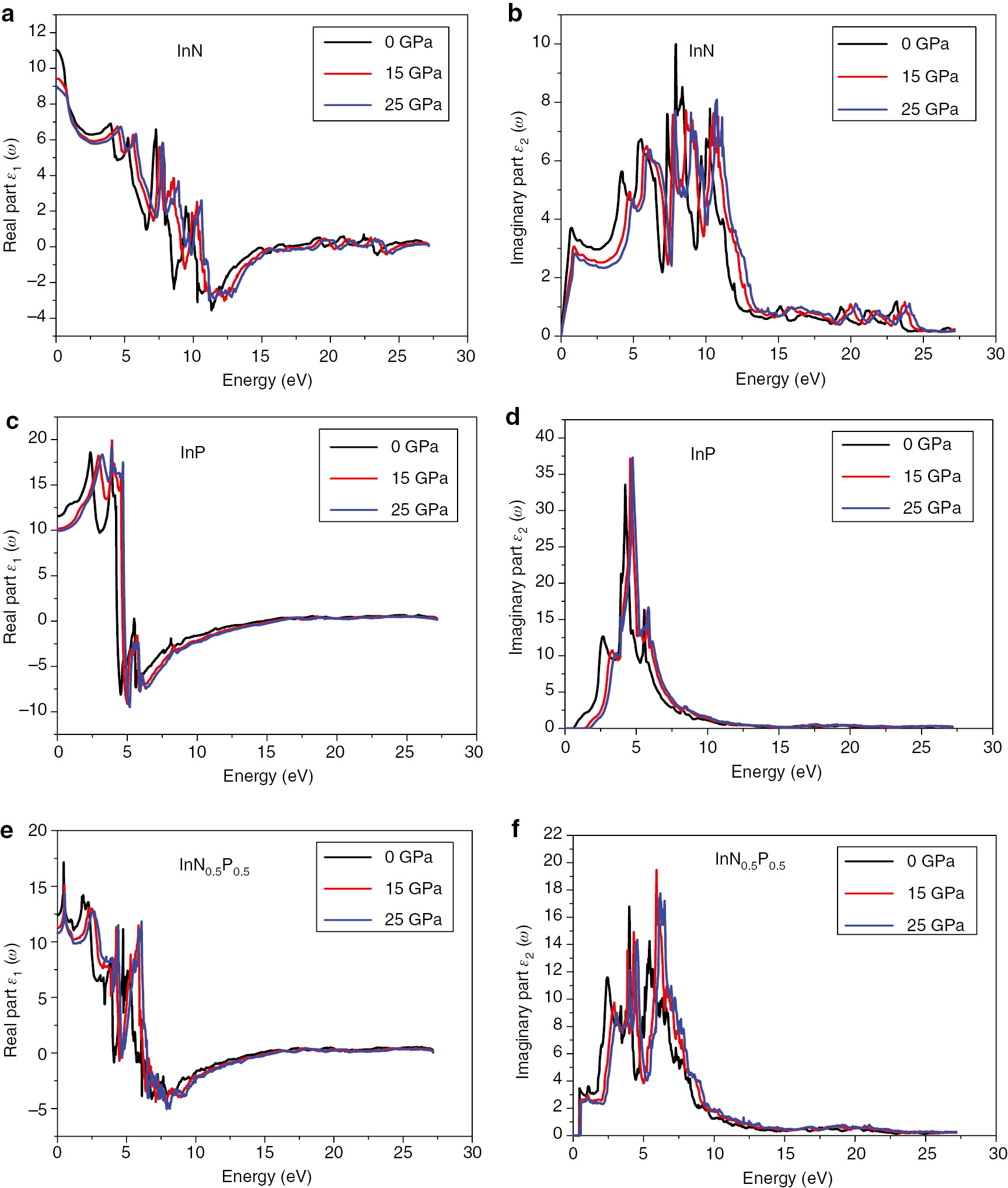
The dielectric function of (a, b) InN, (c, d) InP and (e, f) InN0.50P0.50 compounds under hydrostatic pressure at 0.0, 15, and 25 GPa.
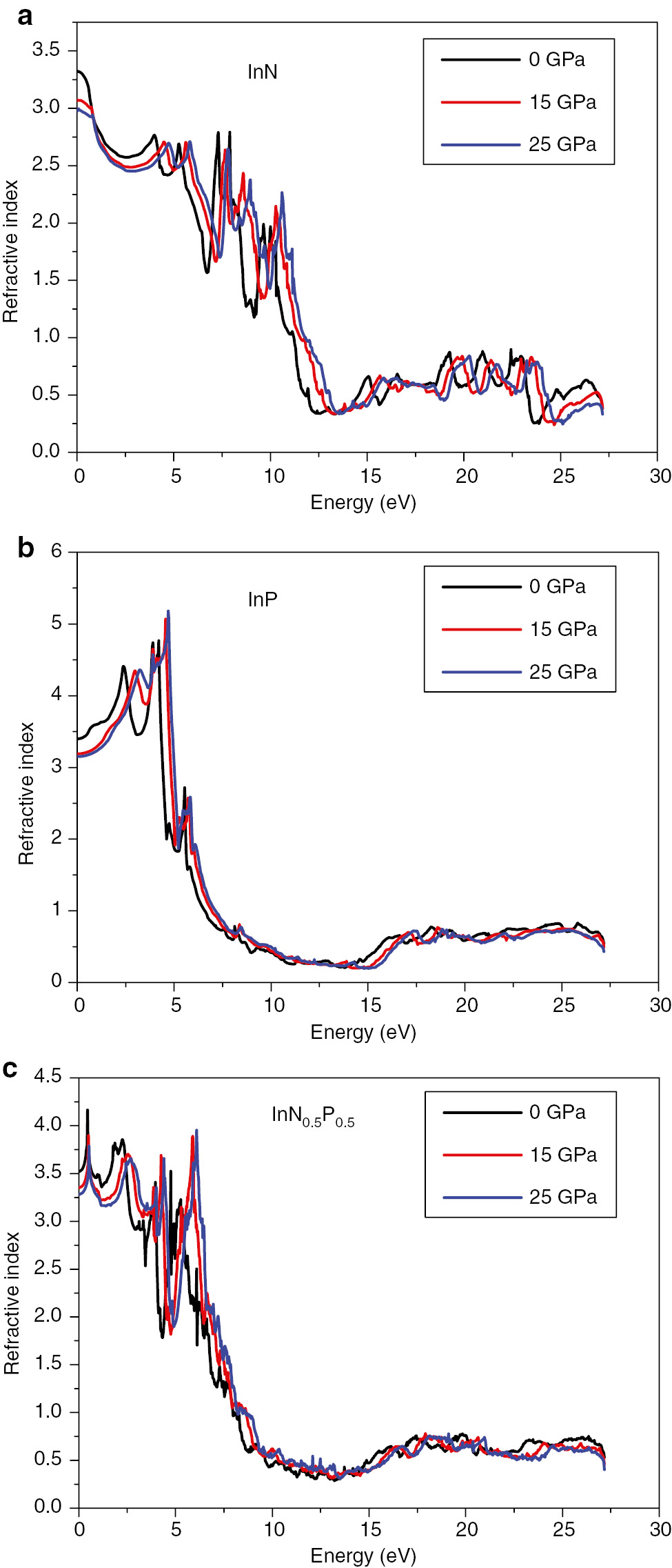
The refractive index of (a) InN, (c) InN0.50P0.50, and (b) InP compounds under hydrostatic pressure at 0.0, 15, and 25 GPa, respectively.
In Figure 11, we present both the effect of the pressure and the nitride composition on the refractive index. The examination of the curve given in Figure 11 shows that the refractive index decreases upon increasing the pressure in the considered range and the same observation when regarding the composition increasing.
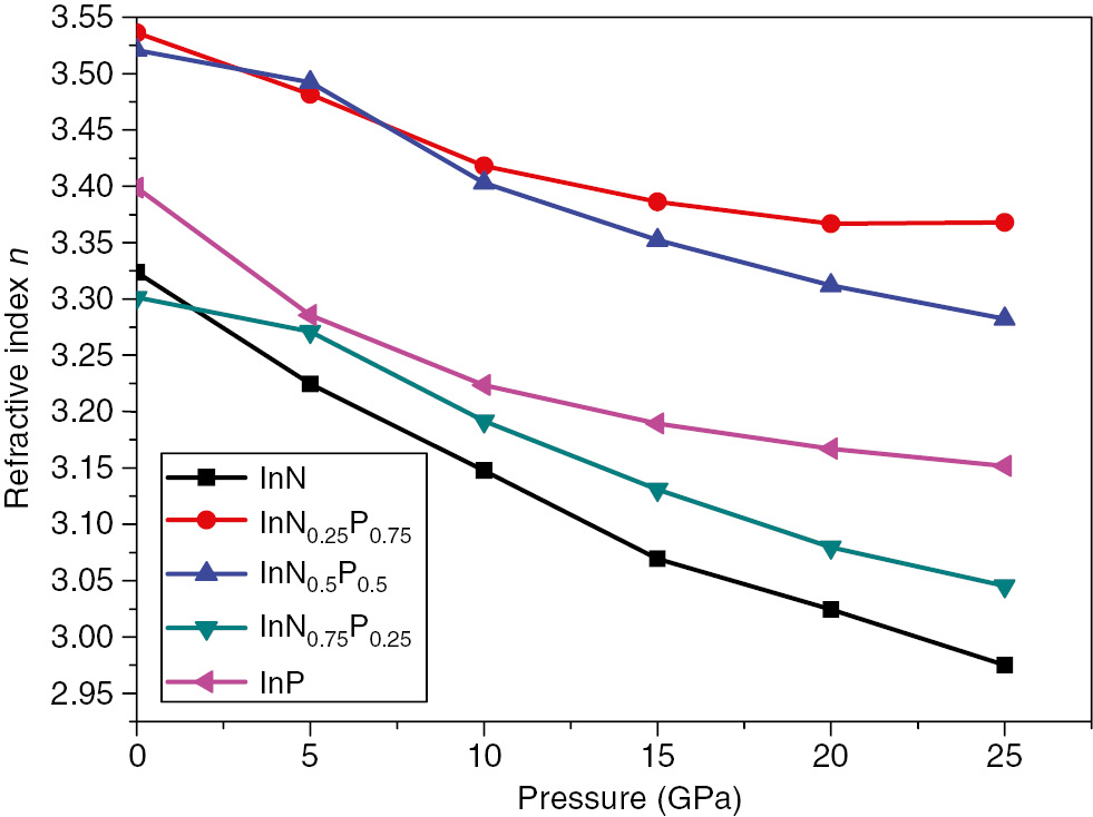
The refractive indices variation versus pressure of the InNxP1–x alloys at different composition of x.
Knowing that the energy loss function is a primordial tool for the investigation of different aspects of materials [44]. Electron energy loss function for InN, InP, and InN0.50P0.50 under pressure are depicted in Figure 12. We observe from this figure that for a photon with energy lesser than the band gap of the considered compound no energy loss occurs and this means no scattering happens. In the intermediate energy range, inelastic scattering is observed and the loss energy value is maximal. The major peaks for a pressure equal to zero are located at 23.82, 14.61, and 13.90 eV for InN, InP, and the InN0.50P0.50, respectively. These peaks in the energy loss spectrum are shifted to higher energy under pressure and correspond to plasma resonance and the corresponding frequency is the plasma frequency.
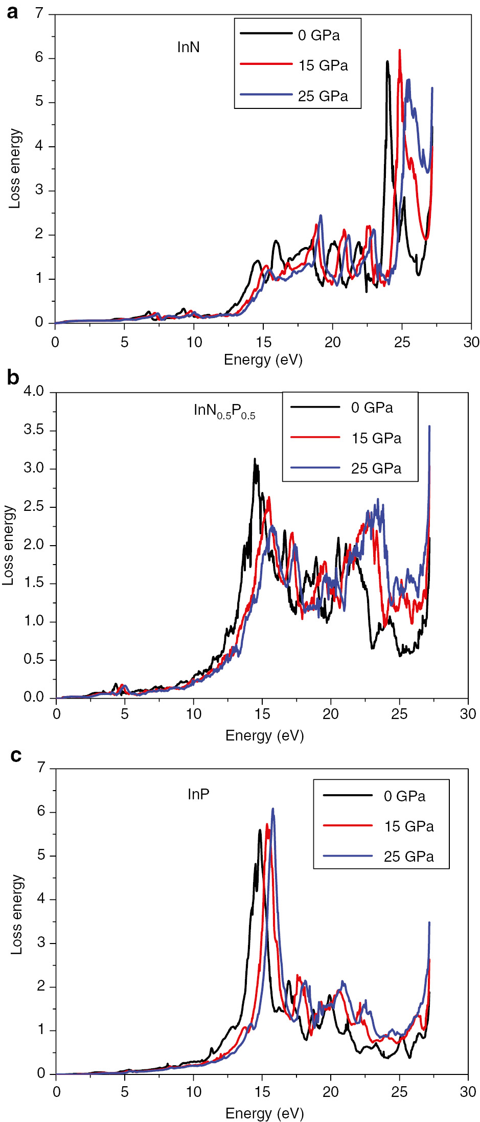
Energy loss of (a) InN, (c) InP, and (b) InN0.50P0.50 compounds under pressure of 0.0, 15, and 25 GPa, respectively.
6 Conclusion
The structural, electronic, and optical properties of zinc-blende InN, InP, and InNxP1–x solid solutions have been carried out using the FP-LAPW method within DFT theory. We have considered the effect of pressure variations on the direct and indirect energy band gaps and optical properties of the InN, InP, and InNxP1–x compounds. The conclusions drawn from this study are as follows:
The lattice constant of the InNxP1–x decreases when increasing the concentration of nitride and the bulk modulus increases with the increase in the concentration x.
The direct energy band gaps decrease upon increasing the nitride composition x. The InNxP1–x presents a direct band gap for all composition x.
In the considered pressure range, the ternary alloy InNxP1–x presents direct band gap energy for each composition and we observe a small increasing for both direct and indirect band gap energies versus pressure.
Under pressure, the structures of the optical parameters of both binary compounds and their ternary InNxP1–x solid solution present a good optical stability.
References
[1] L. Ley, R. A. Pollak, F. R. McFeely, S. P. Kowalczyk, and D. A. Shirley, Phys. Rev. B 9, 600 (1974).10.1103/PhysRevB.9.600Search in Google Scholar
[2] D. E. Aspnes and A. A. Studna, Phys. Rev. B 27, 985 (1983).10.1103/PhysRevB.27.985Search in Google Scholar
[3] C. M. Herzinger, P. G. Snyder, B. Johs, and J. A. Woollam, J. Appl. Phys. 77, 1715 (1995).10.1063/1.358864Search in Google Scholar
[4] A. G. Bhuiyan, A. Hashimoto, and A. Yamamoto, J. Appl. Phys. 94, 2779 (2003).10.1063/1.1595135Search in Google Scholar
[5] J. Wu, W. Walukiewicz, K. M. Yu, J. W. Ager III, E. E. Haller, et al., Appl. Phys. Lett. 80, 3967 (2002).10.1063/1.1482786Search in Google Scholar
[6] Z. Boussahla, B. Abbar, B. Bouhafs, and A. Tadjer, J. Solid State Chem. B 178, 2117 (2005).10.1016/j.jssc.2005.03.047Search in Google Scholar
[7] A. Ben Fredj, M. Debbichi, and M. Said, Microelectronic J. 38, 860 (2007).10.1016/j.mejo.2007.07.002Search in Google Scholar
[8] K. H. Hellwege and O. Madelung, Landolt- Bornstein, Semiconductors: (Physics of Group IV Elements and III–V Compounds). New Series, Group III, 17, Pt. a Springer Verlag, Berlin 1982, p. 602.Search in Google Scholar
[9] M. Kondow, T. Kitatani, S. Nakatsuka, M. C. Larson, K. Nakahara, et al., IEEE J. Sel. Top. Quant. Elect. 3, 719 (1997).10.1109/2944.640627Search in Google Scholar
[10] M. Kondow, T. Kitatani, M. C. Larson, K. Nakahara, K. Uomi, et al., J. Cryst. Growth 188, 255 (1998).10.1016/S0022-0248(98)00060-8Search in Google Scholar
[11] D. J. Friedman, J. F. Geisz, S. R. Kurtz, D. Myers, and J. M Olson, J. Cryst. Growth 195, 409 (1998).10.1016/S0022-0248(98)00561-2Search in Google Scholar
[12] S. R. Kurtz, A. A. Allerman, E. D. Jones, J. M. Gee, J. J. Banas, et al., Appl. Phys. Lett. 74, 729 (1999).10.1063/1.123105Search in Google Scholar
[13] L.-W. Wang, L. Bellaiche, S.-H. Wei, and A. Zunger, Phys. Rev. Lett. 80, 4725 (1998).10.1103/PhysRevLett.80.4725Search in Google Scholar
[14] A. Lindsay and E. P. O’Reilly, Solid State Commun. 112, 443 (1999).10.1016/S0038-1098(99)00361-0Search in Google Scholar
[15] M. Aslan, A. H. Reshak, B. G. Yalcin, S. Bagci, and M. Ustundag, Philos. Mag. 96, 991 (2016).10.1080/14786435.2016.1149248Search in Google Scholar
[16] S. M. Sze, Physics of Semiconductor Devices, Wiley, New York 1981.Search in Google Scholar
[17] P. Blaha, K. Schwarz, G. K. H. Madsen, D. Kvasnicka, J. Luitz, Wien2k, An Augmented Plane Wave Plus Local Orbital Program for Calculating Crystal Properties, Vienna University of Technology, Vienna, Austria 2001.Search in Google Scholar
[18] K. Schwarz and P. Blaha, Comput. Mater. Sci. 28, 266 (2003).10.1016/S0927-0256(03)00112-5Search in Google Scholar
[19] F. D. Murnaghan, Proc. Natl. Acad. Sci. U.S.A. 30, 244 (1944).10.1073/pnas.30.9.244Search in Google Scholar PubMed PubMed Central
[20] D. Koller, F. Tran, and Blaha, Phys. Rev. B 85, 1–8 (2012).10.1103/PhysRevB.85.155109Search in Google Scholar
[21] H. Shi and Y. Duan, Phys. Lett. A373, 165 (2008).10.1016/j.physleta.2008.11.010Search in Google Scholar
[22] A. Abdiche, H. Abid, R. Riane, and A. Bouaza, Acta Phys. Poloni. A 117, 924 (2010).10.12693/APhysPolA.117.921Search in Google Scholar
[23] M. I. Ziane, B. Zouaoui, T. Ouhrni, and B. Hamza, Mater. Sci. Semiconduct. Proc. 30, 181 (2015).10.1016/j.mssp.2014.08.039Search in Google Scholar
[24] J. Serrano, A. Rubio, E. Hernandez, A. Munoz, and A. Mujica, Phys. Rev. B 62, 16612 (2000).10.1103/PhysRevB.62.16612Search in Google Scholar
[25] R. Ahmed, S. J. Hashem Far, H. Akbarzadeh, M. Ahmed, and F. E. Aleem, Comput. Mater. Sci. 39, 580 (2007).10.1016/j.commatsci.2006.08.014Search in Google Scholar
[26] S. Q. Wang and H. Q. Yes, Phys. Rev. B 66, 235111 (2002).10.1103/PhysRevB.66.235111Search in Google Scholar
[27] W. Shen and A. Zunger, Phys. Rev. B 60, 5404 (1999).10.1103/PhysRevB.60.5404Search in Google Scholar
[28] M. Guemou, B. Bouhafs, A. Abdiche, R. Khenata, Y. Al Douri, et al., Physica B 407, 1292 (2012).10.1016/j.physb.2012.01.132Search in Google Scholar
[29] L Vegard, Zeitschrift Fur Physik 5, 17 (1921).10.1007/BF01349680Search in Google Scholar
[30] F. Bechstedt and R. Del Sole, Phys. Rev. B 38, 7710 (1988).10.1103/PhysRevB.38.7710Search in Google Scholar PubMed
[31] D. Jenkins, Properties of Group III-Nitrides (Ed. J. H. Edgar), EMIS Data Reviews 11, INSPEC, London 1994, p. 10233.Search in Google Scholar
[32] P. Rochon and E. Fortin, Phys. Rev. B 12, 5803 (1975).10.1103/PhysRevB.12.5803Search in Google Scholar
[33] O. Madelung and M. Schulz, Londolt-Bornstein: numerical data and functional relationships in science and technology. Cryst Solid State Phys, 17a. Springer-Verlag, Berlin 1987.Search in Google Scholar
[34] S. Adachi, Properties of Semiconductor Alloys: Group-IV, III–V and II–VI Semiconductors, John Wiley & Sons, Ltd., UK 2009, p 307.10.1002/9780470744383.ch10Search in Google Scholar
[35] T. Ouahrani, A. H. Reshak, R. Khenata, B. Amrani, M. Mebrouki, et al., J. Solid State Chem. 183, 46 (2010).10.1016/j.jssc.2009.09.034Search in Google Scholar
[36] Z. Usman, C. Cao, and T. Mahmood, Physica B 430, 67 (2013).10.1016/j.physb.2013.07.031Search in Google Scholar
[37] Z. Feng, H. Hu, S. Cui, and W. Wang, Physica B: Condensed Matter 404, 2103 (2009).10.1016/j.physb.2008.11.076Search in Google Scholar
[38] R. Ahuja, S. Auluck, O. Eriksson, J. M. Wills, and B. Johansson, Solid State Commun. 104, 249 (1997).10.1016/S0038-1098(97)00287-1Search in Google Scholar
[39] S. K. Tripathy, Opt. Mater. 46, 240 (2015).10.1016/j.optmat.2015.04.026Search in Google Scholar
[40] S. Berrah, Phys. Scr. 75, 414 (2007).10.1088/0031-8949/75/4/006Search in Google Scholar
[41] S. K. Tripathy, Opt. Mat. 46, 240 (2015).10.1016/j.optmat.2015.04.026Search in Google Scholar
[42] S. Adachi, Properties of Group III–V and II–VI Semiconductors, Wiley, New York 2005, (Chapter 2).10.1002/0470090340Search in Google Scholar
[43] P. E. Van Camp, V. E. Van Doren, and J. T. Devreese, Phys. Rev. B 41, 1598 (1990).10.1103/PhysRevB.41.1598Search in Google Scholar
[44] S. Loughin, R. H. French, L. K. Noyer, W. Y. Ching, and Y. N. Xu, J. Phys. D 29, 1740 (1996).10.1088/0022-3727/29/7/009Search in Google Scholar
©2016 Walter de Gruyter GmbH, Berlin/Boston
Articles in the same Issue
- Frontmatter
- A Few New 2+1-Dimensional Nonlinear Dynamics and the Representation of Riemann Curvature Tensors
- First-Principle Study of the Structural, Electronic, and Optical Properties of Cubic InNxP1–x Ternary Alloys under Hydrostatic Pressure
- Bäcklund Transformation and Soliton Solutions for a (3+1)-Dimensional Variable-Coefficient Breaking Soliton Equation
- Analytical Solitons for Langmuir Waves in Plasma Physics with Cubic Nonlinearity and Perturbations
- Generalized Klein-Gordon and Dirac Equations from Nonlocal Kinetic Approach
- Fractional Zero-Point Angular Momenta in Noncommutative Quantum Mechanics
- A Crossover from High Stiffness to High Hardness: The Case of Osmium and Its Borides
- Impact of Entropy Generation on Stagnation-Point Flow of Sutterby Nanofluid: A Numerical Analysis
- High-Frequency Waves in a Random Distribution of Metallic Nanoparticles in an External Magnetic Field
- Differential Invariants of the (2+1)-Dimensional Breaking Soliton Equation
- Asymptotic Analysis to Two Nonlinear Equations in Fluid Mechanics by Homotopy Renormalisation Method
- Massive Particle Reflection from Moving Mirrors