Tin chalcogenides – a group of multi utility inorganic materials
-
Vimal K. Jain

 und
Gotluru Kedarnath
und
Gotluru Kedarnath

Abstract
Remarkable and unique properties of main group chalcogenides have been exploited for diverse applications owing to their semiconducting properties with a wide range of band gaps and high absorption coefficients. The scope and horizon of their utility is further expanded by modulating the size to nanometre dimensions as well as the number of layers in 2-D layered materials. A number of these materials, like CdTe, CuInSe2, HgCdTe, In2S3, PbTe, Bi2Te3, etc., are used in several commercial devices, but either their scarce availability in the earth crust or toxicity limits their large-scale utilization. Tin forms several binary, ternary and quaternary chalcogenides which show desirable semiconducting properties. Different compositions and phases exhibit distinct conductivity (p/n-type) and energy band gaps. The band gap energy varies greatly from narrow-band (∼0.2 eV) to wide-band (>2.0 eV) depending on the tin chalcogenide. Benign nature and cost effectiveness of tin makes it the most suitable candidate among main group materials. With the flexible tuning of physical and chemical properties, accomplished through different strategies, versatile applications of tin chalcogenides can be realized. This review highlights recent advances on different facets of tin chalcogenide chemistry with their applications in diverse areas.
Abbreviations
- AACVD
-
Aerosol assisted chemical vapor deposition
- Bz
-
Benzyl
- CVD
-
Chemical vapor deposition
- CZTS
-
Copper zinc tin sulfide (Cu2ZnSnS4)
- DDT
-
1-Dodecane thiol
- DSSC
-
Dye sensitized solar cell
- HDA
-
Hexadecyl amine
- LIB
-
Lithium-ion battery
- LPCVD
-
Low-pressure chemical vapor deposition
- NC
-
Nanocrystal
- OA
-
Oleic acid
- ODE
-
1-Octadecene
- OLA
-
Oleyl amine
- PCE
-
Power conversion efficiency
- rGO
-
Reduced graphene oxide
- SSMP
-
Single source molecular precursor
- TOP
-
Trioctylphosphine
- TOPO
-
Trioctylphosphine oxide
1 Introduction
Metal chalcogenides represent a group of important and versatile family of inorganic materials of great technological and biomedical relevance and find wide ranging applications in optoelectronic devices, 1 thermoelectric devices, 2 , 3 energy harvesting, 4 , 5 storage devices, 6 catalysts, 7 electromagnetic interference (EMI) shielding 8 , 9 , 10 and sensing platforms, etc. Different classes of metal chalcogenides, viz., binary (ME, ME2, M2E3 where M = metal and E = S, Se, Te), ternary (e.g., CuInSe2, 11 CuInTe2 8 and quaternary (e.g., Cu2ZnSnS4 12 ) can readily be identified for these applications. Several of them show semiconducting properties. Their physical, chemical, and electronic properties can be further modified by reducing their crystallite size to nanometre dimensions, thus further expanding the scope and horizon of their utility. Brus has demonstrated in the mid-1980s that the optical and electronic properties of bulk CdS differ markedly in nano regime in a size dependent manner and has been attributed to quantum confinement effects. 13 , 14 This discovery revolutionized the area of metal chalcogenides in the nano regime.
The discovery of graphene by Geim and Novoselov 15 , 16 further added a new dimension to metal chalcogenide research, in particular transition metal dichalcogenides (TMDs, ME2). Like graphite, many TMDs have a layered structure. 17 , 18 Each layer (thickness of 6–7 Å) is composed of three covalently bound atoms (E-M-E) where two chalcogen atoms encapsulate the metal atom. 19 , 20 Each layer is connected by van der Waals bonds which are slightly longer than graphite (3.4 Å) and vary markedly in different materials. The weak van der Waals forces between the layers can facilitate exfoliation of TMDs into the sheet of single layer. These TMDs exhibit varied electronic properties ranging from insulating, semiconducting, semi-metallic, metallic to superconducting. 21 The unique and remarkable properties of ultrathin layers of TMDs, distinct from their 3-D counterparts, make them potentially interesting candidates for numerous applications. 22 , 23 , 24 Interestingly, several main group chalcogenides, like TMDs, also have layered structures which can be exfoliated. 25 The binary layered main group chalcogenides with formal stoichiometries of ME, ME2 and M2E3 have covalently bonded 2D stacking units of E−M−M−E, E−M−E and E−M−E−M−E atomic layers, respectively. 22 The binding energy of SnS and SnSe layers has been calculated as 30 and 10 meV Å−2, respectively making them easily exfoliable materials and by changing the number of layers band gap can be tuned over a large range (0.6 and 0.4 eV for SnS and SnSe, respectively). 26 Depending on the metal-chalcogen coordination environment and stacking order within the individual layers different polymorphic structures differing in symmetries can exist. 27
The interest in main group metal chalcogenides and also those of zinc triad [for being formed with the filled d 10 configuration 28 ] has expanded due to their possible applications in electronics and energy-related demands which is driven by their adaptable electronic properties, semiconducting behaviour and high thermoelectric performance. A number of them are now used in commercial devices. These include CdTe and CuInSe2 for photovoltaic solar cells, 4 , 5 HgCdTe (MCT) infrared detectors, 29 In2S3 as passivating and buffer material, 30 PbTe, Bi2Te3 for thermoelectric devices. 2 , 31 , 32 , 33 Although several of them are used in commercial devices, most of them are based on elements which are either scarcely available in the earth crust (e.g., In, Te) or toxic (e.g., Cd, Hg, Pb) in nature, thus necessitating for alternate materials with similar properties. Tin, which forms several binary, ternary and quaternary chalcogenides of desirable properties, does not have such limitations and therefore emerges as the most suitable candidate among the main group chalcogenide materials. Furthermore, its cost effectiveness and benign nature gives added advantage to their applications. Accordingly, in this review, different facets of tin chalcogenide chemistry with their applications are presented so as to further accelerate the exploration of tin chalcogenides.
2 Tin chalcogenide crystal structures
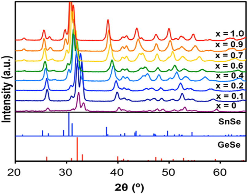
Tin forms numerous chalcogenides which can be clubbed into binary, ternary and quaternary compounds depending on the number of constituent elements (Figure 1). These compounds in general exhibit semiconducting properties with direct and/or indirect band structures. Substitution of constituent elements in the binary system has been practiced for engineering the band-gap and band-structures of semiconductor compounds. Both vertical -substitution (substituting an element by another in the same group of the Periodic Table) and cross-substitution, established for fabricating chalcogenide materials, 34 , 35 , 36 , 37 have been developed to design several ternary and quaternary tin chalcogenides (Scheme 1).
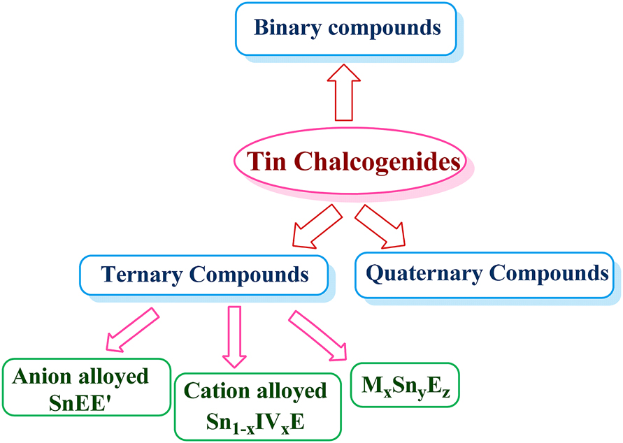
Different types of tin chalcogenides, where ‘IV’ is any group IV element other than tin and E = S, Se or Te.
Cross-substitution of elements in binary chalcogenides to fabricate ternary and quaternary chalcogenide materials.
2.1 Binary tin chalcogenide materials
Binary tin chalcogenides exist in two stoichiometries, viz. SnE (E = S, Se, Te) and SnE2 (E = S or Se) except for Sn2S3 which possesses a non-equilibrium phase. In general, binary tin chalcogenides are layered compounds and crystallize into cubic, hexagonal, trigonal and orthorhombic space groups (Table 1). Thermodynamically stable phase of monochalcogenides, α-SnS and α-SnSe, have orthorhombic Pnma structure at room temperature. The structure of SnS consists of double layers of tin and sulfur atoms, similar to deformed NaCl structure, where each layer is bonded through weak van der Waals forces. The Sn2+ ion adopts a distorted octahedral configuration defined by six sulfur atoms. The distortion can be attributed to the existence of three short and three long Sn–S bonds. 38 The orthorhombic structure of SnSe is similar to three-dimensional deformed rock-salt structure in which Sn and Se atoms are part of layered structure. The two planes of Sn–Se chains are zipped through van der Waal interactions. The orthorhombic SnSe unit cell consists of distorted SnSe7 units in which there are three short and four long Sn–Se bonds. The Sn(II) lone pair occupies one of the symmetrical sites and imparts its effect to deform the crystal structure. 39 , 40 The double layer structure of SnE (E = S or Se) imparts anisotropic properties to these materials. 39 Interestingly, both α-SnS and α-SnSe (orthorhombic, space group Pnma) undergo phase transition above 600 °C and at 523 °C, respectively to orthorhombic Cmcm (β-SnE) with the shifting of Sn and E along (100) direction. 41 , 42 The phase transition of SnE (E = S or Se) from α-to β-form has been reported as second order transition of displacement type. 43 In addition to orthorhombic structures, SnS also has a metastable cubic structure, 44 while for SnSe a cubic phase has been identified recently. Different crystallographic structures of SnE are depicted in Figure 2. 45 , 46
Crystal structures of binary tin chalcogenides.
| SnxEy | Crytal system | Space group |
|---|---|---|
| α-SnS | Orthorhombic | Pnma (62) |
| β-SnS | Orthorhombic | Cmcm (63) |
| π-SnS | Cubic | P213 (198); F-43m (216); Fm-3m (225) |
| SnS2 | Hexagonal | P63 mc (186) |
| Trigonal | P-3m1 (164) | |
| Cubic | Fd-3m (227) | |
| Sn2S3 | Orthorhombic | Pnma (62) |
| α-SnSe | Orthorhombic | Pnma (62) |
| β-SnSe | Orthorhombic | Cmcm (63) |
| π-SnSe | Cubic | Fm-3m (225); P213 (198) |
| SnSe2 | Orthorhombic | Pnma (62) |
| Trigonal | P-3m1 (164) | |
| α-SnTe | Orthorhombic | Pnma (62) |
| β-SnTe | Cubic | Fm-3m (225); F-43m (216); Pm-3m (221) |
| γ-SnTe | Orthorhombic | Pnma (62) |

Under atmospheric conditions, SnTe crystallizes in a cubic structure with space group Fm-3m. Tin and tellurium atoms occupy the octahedral sites. For the octahedral coordination, each atom should have on an average six valence electrons per atom, but both Sn and Te have only three valence electrons. Because of inadequate number of valence electrons, the various electronic configurations resonate resulting in soft Sn–Te bonding which subsequently interacts with the lone pair of tin to give distorted crystal structure. This phase is stable up to 727 °C but below 100 K rhombohedral phase of SnTe exists. 47 , 48 However, under pressure the cubic phase of SnTe changes to an orthorhombic structure (γ-SnTe) with Pnma space group.
Ground state SnS2 has the trigonal crystal structure belonging to P-3m1 space group. 49 The structure comprises edge sharing octahedral SnS6 units where Sn4+ ions are surrounded by six sulfur atoms. The SnS6 units lie along the c-axis. Each unit is connected with each other by weak van der Waals interactions (Figure 3). 45 Similarly, SnSe2 crystallizes in a trigonal system in a P-3m1 space group and can also adopt orthorhombic structure. 49 Thermogravimetric analysis of SnS2 and SnSe2 revealed that both compounds decompose at 570 and 340 °C, respectively to the corresponding tin monochalcogenide (SnE) with the elimination of sulfur/selenium. 50 The Sn2S3 is a mixed valent tin chalcogenide. It adopts a ribbon-like structure where the Sn2+ and Sn4+ ions are surrounded by sulfur atoms in a trigonal bipyramidal and octahedral geometries, respectively. It shows n-type conductivity. Depending on preparative method, band gap energy varies between 0.95 and 2.2 eV.
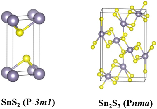
Crystal structures of SnS2 and Sn2S3 (tin in grey and sulfur in yellow) (reproduced from American Chemical Society). 45
2.2 Structure related properties of binary tin chalcogenides
Binary tin chalcogenides constitute an important class of 2D layered materials by virtue of its crystallographic structure. These tin chalcogenides have covalent bonding within the planes whilst having interlayer connection through van der Waals forces. Scion of these weak forces results in slices of 2D layered sheets. For instance, orthorhombic SnS and SnSe which has distorted NaCl crystal structure exhibit aforementioned bonding leading to 2D layered materials. Here, lone pair electrons of Sn(II) lodges at one of the symmetrical sites leading to deformed structure which further imparts anisotropic nature to these materials. 39 However, in cubic phase (rock salt and zinc blende structures) of SnS and SnSe, asymmetric bonding dictated by lone pair of Sn2+ causes both tin and chalcogen atoms to occupy four discrete crystallographic sites. While SnTe preferably existing in cubic structure get distorted due to interaction of delocalized electron cloud of soft Sn–Te bonding with lone pairs of Sn2+. This results in the formation of 0D materials preferably in case of SnTe materials while SnTe sheets can be produced by growth directing methods like template mediated anion exchange 51 and vapor-liquid-solid-methods, 52 etc.
Like tin monochalcogenides, tin dichalcogenides (SnE2), also exhibit CdI2-type layered structure wherein tin and chalcogen are covalently bonded within the layer and inter-layers are held together by van der Waals forces. This type of structure drives the formation of 2D sheets. Furthermore, sesquisulfide i.e. Sn2S3 also assumes ribbon like structures. Owing to their layered structure, tin chalcogenides display remarkable properties which make them potential electrode material for energy storage devices. While anisotropic structure, resonant bonding and local structural distortion resulting in anharmonicity and hence lowering of thermal conductivity brand them as good thermoelectric materials. Additionally, suitable band gap and high absorption coefficient for harvesting solar energy combined with effective carrier mobility proffers tin chalcogenides as an efficient active material for photovoltaics, 39 , 53 and optoelectronics. 39 Features such as narrow band gap, heavy constituent elements and substantial spin–orbit coupling project them as an important class of topological materials. 54
2.3 Ternary tin chalcogenide materials
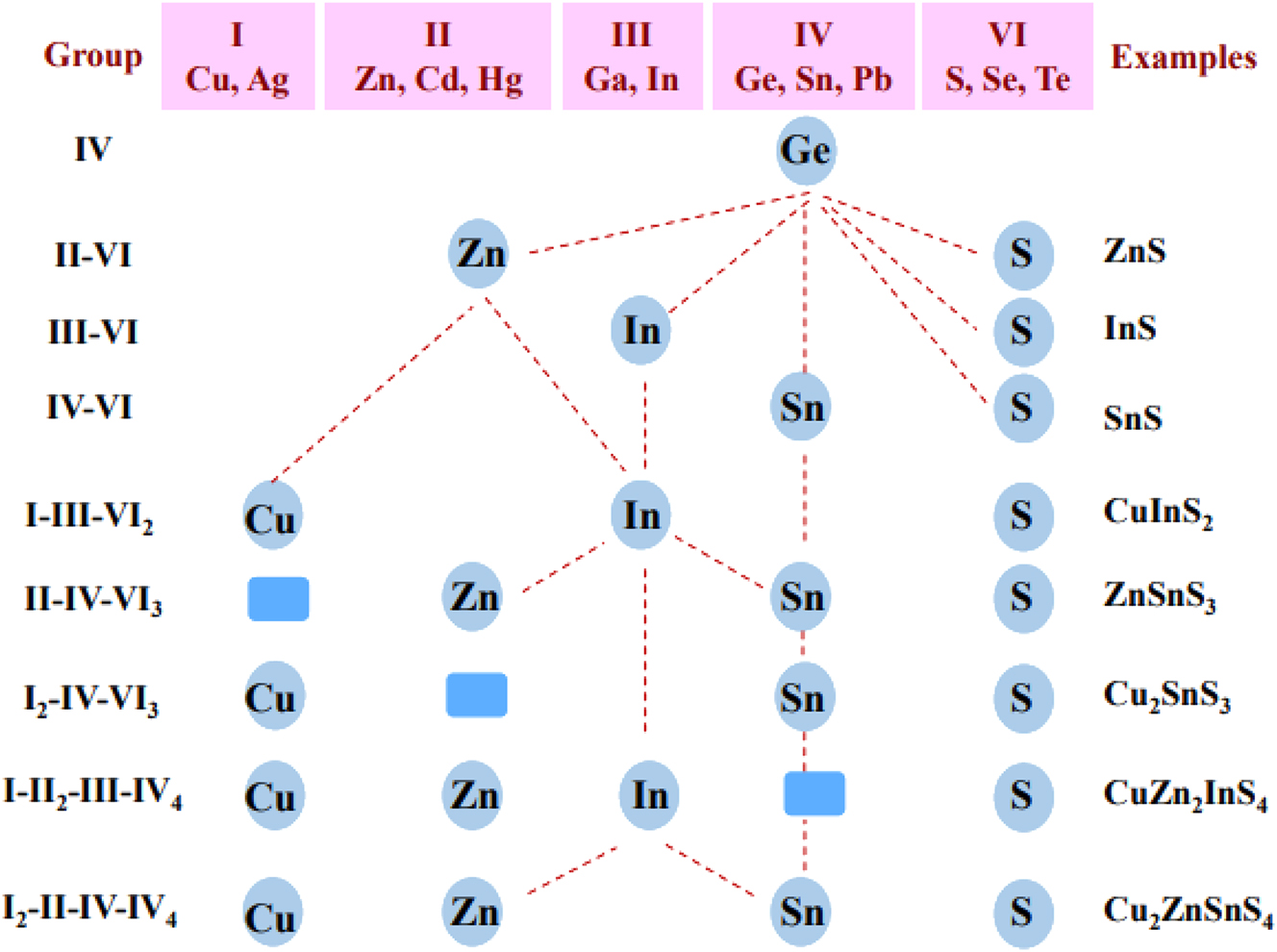
There are several ternary tin chalcogenides, such as Cu2SnE3 (E = S or Se), Cu2SnSe4, ZnSnS3, etc. In the Cu–Sn–S Gibbs phase triangle, several ternary compounds have been identified which include orthorhombic Cu4SnS4, Cu2SnS3, orthorhombic or tetragonal Cu3SnS4 and more complex structures, Cu4SnS4, Cu4SnS6, Cu4Sn7S16 and Cu4Sn15S32, etc. 55 , 56 These phases are mainly p-type semiconductors except Cu4Sn7S16 which is an n-type semiconductor, 57 although some metallic phases like orthorhombic Cu3SnS4 (a mixed valence compound) and rhombohedral Cu4SnS6 are also encountered. Among ternary systems, Cu2SnE3 (E = S and Se) have received much attention. 56 These compounds exist in various polymorphic forms like cubic, tetragonal, hexagonal, monoclinic, triclinic, and orthorhombic and can undergo phase transition at different temperatures. For instance, Cu2SnS3 at low temperature exists in a tetragonal chalcopyrite structure which can be converted into the metastable zinc blende structure at 780 °C, and wurtzite structure at 856 °C. 55 The formal oxidation states of Cu, Sn and E in Cu2SnE3 have been deduced as +1, +4 and −2, respectively from X-ray photoelectron spectroscopy. 58
2.4 Quaternary tin chalcogenide materials
The quaternary tin chalcogenide compounds, Cu2MSnE4 (M = Zn, Cd, Mn, Fe, Co, Ni, etc., E = S or Se) exist in different polymorphs of closely related crystallographic structures. 59 , 60 , 61 , 62 In these structures every sulfur anion is bound with four cations (2Cu+, M2+ and Sn4+) and vice versa and the cations occupy different positions in the closely related structures. Depending on the preparative method, these compounds can crystallize into thermodynamically stable body-centered tetragonal kesterite, stannite and primitive mixed Cu–Au (PMCA) phases 63 and a metastable wurtzite phase (hexagonal) 62 (Figure 4). Besides these structures, wurtzite derived structures, e.g., wurtzite–kesterite and –stannite phases, can also form. 64 , 59 , 65 Different CZTS phases can form at different temperatures. 66 The kesterite phase, thermodynamically the most stable structure, 67 can undergo phase transition into disordered kesterite 260 °C, but at much elevated temperatures (866−1,002 °C) can transform into sphalerite phase–a fully disordered cubic structure. 60 Similarly, annealing of metastable wurtzite CZTS nanorods (diameter and length: 9 ± 0.5 and 35 ± 1 nm, respectively) at 400 °C results into kesterite phase within a few seconds. 68 Different phases of CZTS differ only slightly in energy. 69 , 70 , 71 The stannite and PMCA phases are higher in energy by 2.9 and 3.2 meV/atom, respectively than the kesterite phase. 69 , 71 Because of small differences in total energy values and similar lattice constants, kesterite and stannite structures can often co-exist in the synthesized samples.
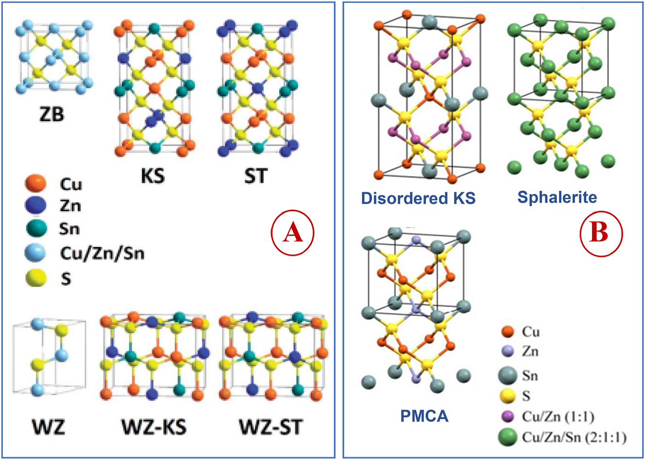
Schematic representation of quaternary Cu2ZnSnS4 structures derived from zinc-blende (ZB) and wurtzite (WZ) phases of binary ZnS (KS = kesterite; ST = stannite; (KS), WZ-KS = wurtzite–kesterite; and WZ-ST = wurtzite–stannite) (adapted from Royal Society of Chemistry 64 (A) and with permission from Royal Society of Chemistry 63 (B).
2.5 Band-gap of metal chalcogenides
Tin chalcogenides are semiconductor materials. Different compositions and phases exhibit distinct conductivity (p/n-type) and energy band gaps. The band gap energy varies greatly from narrow-band (∼0.2 eV) to wide-band (>2.0 eV) depending on the tin chalcogenide. The band structures and band-gaps can be modulated by altering the size of the material to nano dimension, i.e., as nanoparticles/nanocrystals (NCs) (one of the dimensions in the range of 1–100 nm). The band structure can be modified by reducing one of the dimensions of these particles to smaller than the Bohr exciton radius, as a consequence such particles show quantum confinement effect. 64 , 72 , 73 The quantum size effect is manifested in shifting of band gap to higher energy (a blue shift) relative to the band for bulk counterparts (Figure 5). Besides size-effect, physicochemical properties of NCs are also affected by their compositions, morphologies, crystal structures, etc. As several tin chalcogenides have layered structures, they exhibit highly layer-dependent electronic properties. 74 , 75 , 76 , 77 For example, the indirect band gap of bulk SnS2 increases from Eg = 2.18 eV–2.41 eV for the single layer (Table 2). 75 , 76 , 77 The optoelectronic properties of tin chalcogenides, in general for metal chalcogenides, strongly depend on preparative method, size, morphology, phase purity, etc. Due to this reason, the value of band gap energy often differs in different publications. Therefore, selection of a synthesis/deposition of thin film method is of paramount importance for proposed application of the material.
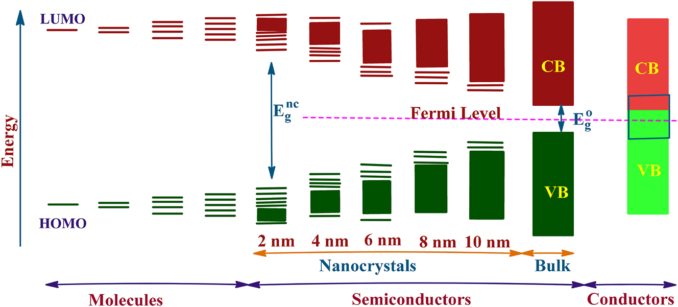
Schematic representation of evolution of energy levels from molecules to semiconductors to conductors. Eg nc and Eg o indicate band energy of nanocrystals and bulk semiconductors.
Indirect and direct band gaps of bulk and few layers of SnE (E = S or Se) 76 , 77 and SnE2 (E = S or Se). 75
| SnEx (x = 1 or 2) | System | E g (indirect) (eV) | E g (direct) (eV) |
|---|---|---|---|
| SnS | Bulk | 1.07 | 1.32 |
| Two-layer | 1.57 | 1.98 | |
| Single-layer | 2.57 | 2.72 | |
| SnSe | Bulk | 0.9 | 1.3 |
| Two-layer | 1.47 | 1.62 | |
| Single-layer | 1.63 | 1.66 | |
| SnTe | Bulk | – | 0.18 |
| SnS2 | Bulk | 2.18–2.28 | 2.56–2.88 |
| Quadra-layer | 2.22 | 2.50 | |
| Tri-layer | 2.29 | 2.54 | |
| Bi-layer | 2.34 | 2.57 | |
| Single-layer | 2.41 | 2.68 | |
| SnSe2 | Bulk | 0.98–1.07 | 1.28–1.84 |
| Quadra -layer | 1.26 | 1.58 | |
| Tri-layer | 1.37 | 1.68 | |
| Bi-layer | 1.51 | 1.83 | |
| Single-layer | 1.69 | 2.04 |
3 Synthesis of metal chalcogenides
Over a period, several synthetic approaches have evolved for the preparation of metal chalcogenides, their nanocrystals, and thin films. 22 , 78 The traditional solid-state synthesis is carried out by reacting constituent elements in required stoichiometric ratio in sealed tubes at high temperatures (>600 °C) and/or high pressure which often yields coarse and aggregated particles. 79 , 80 Several synthetic approaches based on solution-phase and gas-phase processes have emerged due to their high versatility and ease. They do not require extreme conditions of traditional solid-state synthesis. Now nano-materials with high composition and phase purity, crystal phases, precise size (monodispersed material), morphologies, doping defects and surface properties required for the desired applications can be produced with greater reproducibility under moderate reaction conditions. Different synthetic methods can be categorized broadly in two groups, viz. top-down or fabrication method and bottom-up or synthesis approach (Scheme 2). Different synthetic methods might yield products exhibiting different characteristics like physical, chemical, electronic, and surface properties.

Different synthetic approaches for metal chalcogenide nanocrystals.
Bottom-up methods are widely employed for the synthesis of tin chalcogenides owing to the control over broad chemical compositions, morphology, dimension, and crystal phases. 64 , 81 , 82 , 83 , 84 These include: hot-injection synthesis, 85 heat-up synthesis, 86 hydrothermal/solvothermal synthesis, 87 , 88 microwave-assisted processes, polyol methods. In hot injection method a chalcogen precursor containing solution is swiftly added into a hot solution of a metal salt and capping agents, whereas in heat-up method all the reactants (metal precursor, chalcogen precursor, capping agent) are mixed at low temperature in one-pot and subsequently the contents are heated to an appropriate high temperature to trigger the formation of metal chalcogenide. 82 , 84 In hydrothermal (in water)/solvothermal (in non-aqueous solution) methods reaction between metal compounds and chalcogen source is carried out in a sealed autoclave at higher temperature and pressure to promote the formation of crystals. 22 Quaternary semiconductors are usually prepared by hot-injection and heat-up methods. 81 These protocols involve multi-source precursors of metal and chalcogen, and a variety of other reagents to obtain nanomaterials of required compositions. The tin source is realized by its salts such as SnCl2·2H2O, Sn(OAc)2, [Sn{N(SiMe3)2}2], SnCl4·5H2O, Sn(OAC)4, while chalcogen source, E (E = S, Se or Te) is accomplished by Na2S, thiourea, thioacetamide, thiols (1-dodecane thiol, tert-dodecane thiol) or H2S in case of S; selenourea or selenols, SeO2 and Ar2Se2 for Se; Ph2Te2 for Te. Additionally, elemental chalcogen (S, Se, Te) dissolved in a Lewis base like OLA or TOP or in organic solvents, such as ODE, ethylene glycol has also been employed as a chalcogen source.
The multi-source precursor route has its own merits and limitations. For instance, the dual/multiple source method has an advantage of separation of nucleation and growth stages in a controlled fashion as compared to other methods in thermolysis mode and results in an exceptional control over the crystallite size and shape of nanocrystals. However, multiple source precursors in general are toxic, volatile, hygroscopic and often expensive. For instance, H2S used as a sulfur source is toxic, SnCl4 is hygroscopic while [Sn{N(SiMe3)2}2] is air sensitive posing inconvenience in handling. The formation of various secondary phases including binary metal chalcogenides along with elemental metal or chalcogen further aggravates the synthesis protocol using multiple source precursors. For example, synthesis of SnS nanorods by solvothermal method using SnCl2·2H2O and Na2S for LIB anode material, produced the product contaminated with SnS2. 89 For deposition of high-quality thin films, multiple source precursors may prove unreliable for reasons like pre-gas phase reactions, poor stoichiometric control, and formation of defective films due to high deposition temperatures. Furthermore, when the precursors are highly volatile, they afford non-stoichiometric and impure materials as the precursors may volatilize from the reaction container even before its involvement in the reaction. 90
To overcome prevalent deficiencies of dual/multi source precursors method, the use of single source molecular precursors, either in heat-up or hot-injection route, has emerged as a remarkable approach for the synthesis of metal chalcogenides. In this approach pre-existing M-E bonds facilitate in yielding uniformly monodispersed nanoparticles. 91 , 92 , 93 Additionally, most of the prudently designed single-source precursors are air-stable, less toxic and are convenient to handle, purify and characterize. The programmed pre-existing bonds in them help in stoichiometric delivery of material through molecular level mixing. Further, materials with fewer defects can be realized through thoughtful design of SSMPs by judicious selection of ligands to develop precursors which have lower decomposition temperature with cleaner decomposition mechanisms. Additionally, versatility of SSMP is utilized both for the NCs synthesis and for thin films deposition by AACVD technique. Thin films deposition using SSMP in AACVD method is much simpler due to easy precursor delivery and handy processing conditions compared to other conventional CVD method using dual source precursors and eliminates use of toxic, pyrophoric, volatile reagents such as metal alkyl organometallic compounds. SSMP also offers better control over thin film composition and homogeneity due to molecular level pre-mixing of the desired elements in SSMPs.
SSMPs, despite several merits, have their own share of drawbacks such as existence of high nuclearity complexes, tendency to oligomerize which results in decreased solubility in common organic solvents posing difficulty in their purification and characterization. Such complexes usually have high decomposition temperatures compared to monomeric derivatives and can produce several unwanted impurities along with the desirable product due to their incomplete decomposition. The merits of SSMP are also lost if the bonds between the core elements of SSMP are comparable or weaker than those between the core and the organic ligands. Such a SSMP, assumes an unfavourable decomposition path leading to unwanted by-products. For instance, synthesis of SnSe using (Bz3Sn)2Se produced samples contaminated with elemental tin. 94 Another significant problem associated with SSMP having bulkier ligands or SSMPs which undergo improper cleavage often yield products contaminated with carbon impurity.
High-quality thin films of metal chalcogenides are required for various applications like solar cells, thermoelectric devices, etc. Several methods have been developed for deposition of metal chalcogenide thin films (Scheme 3). 95 Spray pyrolysis and chemical vapor deposition methods are most commonly employed for deposition of tin chalcogenide films. CVD has been considered as a promising route to grow high-quality tin chalcogenide thin films in a scalable and controllable manner with desired orientation and morphology. 22 , 93 Owing to the versatility of CVD method, several variants of this technique have been developed in the recent past. These include metal–organic CVD (MOCVD), AACVD, atmospheric pressure CVD (APCVD), low pressure MOCVD (LPMOCVD), etc.
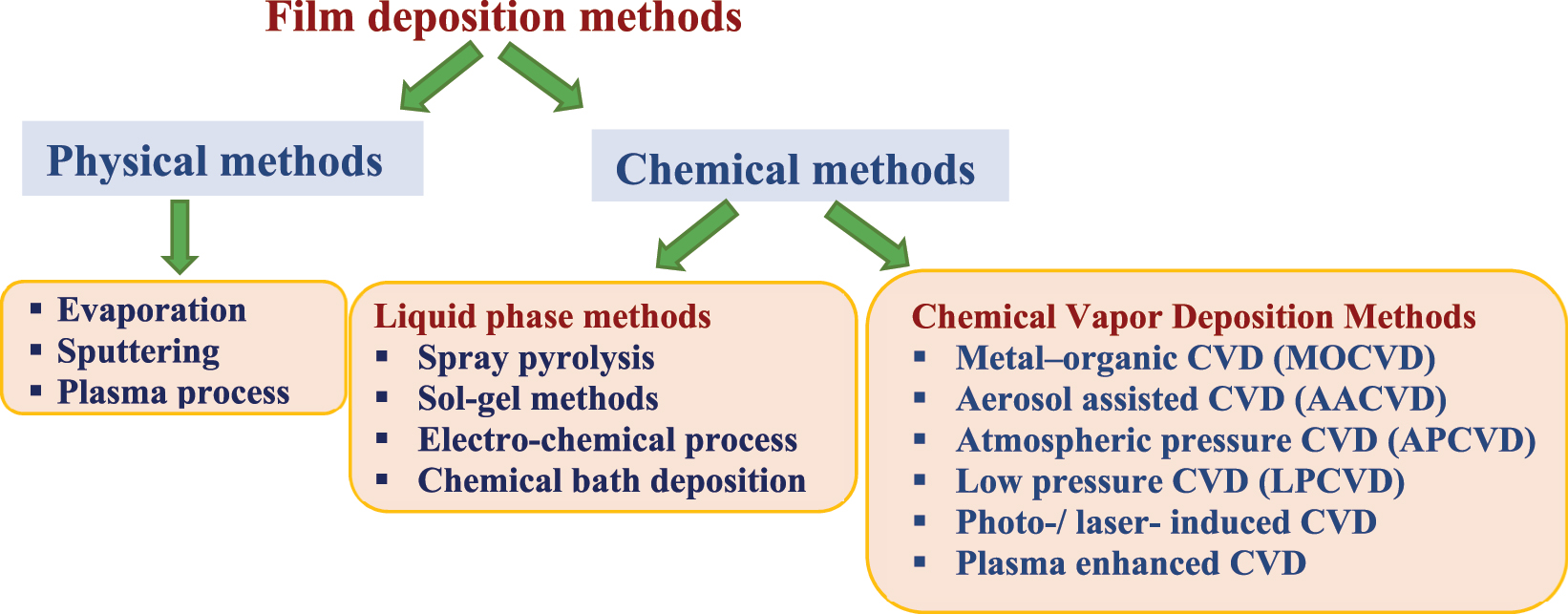
Different deposition methods for metal chalcogenide thin films.
3.1 Synthesis of binary tin chalcogenides
A variety of tin chalcogenolate complexes have been engaged as precursors for binary tin chalcogenide synthesis. Tin complexes in both + 2 and + 4 oxidation states have been used. Complexes of tetravalent tin, at large, have monomeric structures, while tin(II) chalcogenolates of general formula [Sn(ER)2], adopt several coordination geometries, viz. monomeric (e.g., [Sn(SC6H2But 3-2,4,6)2]), 96 dimeric (e.g., [Sn(Sepy)2], 97 [Sn{ESi(SiMe3)3}2]2, 98 trimeric (e.g., [Sn(SC6H3Pri 2-2, 6)2]3) 96 and 1-D polymer (e.g., ∞ 1[Sn(SBun)2] 99 ; ∞ 1[Sn(SBut)2] 100 ; ∞ 1[Sn(EPh)2] (E = S, Se, Te). 101
3.1.1 Tin(II) precursors for the synthesis of tin chalcogenide
Divalent tin chalcogenolates (e.g., ∞ 1[Sn(EPh)2] (E = S, Se, Te), 102 [M(Sepy)2], 97 [Sn{ESi(SiMe3)3}2] (E = S, Se, Te), 98 undergo a single step decomposition to yield ME with concomitant elimination of chalcogeno ethers. The complexes ∞ 1[Sn(EPh)2] start decomposing under a flow of helium gas at 265, 200 and 126 °C for E = S, Se, Te, respectively with the formation of phase pure SnE. 101 The complex [Sn{TeSi(SiMe3)3}2] either under flowing nitrogen at 250 °C or in refluxing toluene affords phase pure SnTe, whereas other complexes, [Sn{ESi(SiMe3)3}2] (E = S or Se) under similar conditions yield SnE contaminated with metallic impurities. 98 Nanocrystals of cubic phase of SnTe have been isolated by rapidly injecting a mixture of [Sn{N{SiMe3)2}2]2 and trioctylphosphine telluride in ODE containing OLA at 150 °C. 102 These SnTe NCs in tetrachloroethylene when evaporated slowly under low pressure resulted in the formation of self-assembled superlattice (Figure 6). The size of NCs varied in the range 4.5–15 nm and can be managed by fine tuning the rate of injection, thermolysis temperature and concentration of OLA in the reaction. The optical band gap values for 7.2 and 14 nm NCs are 0.54 and 0.39 eV, respectively. 102
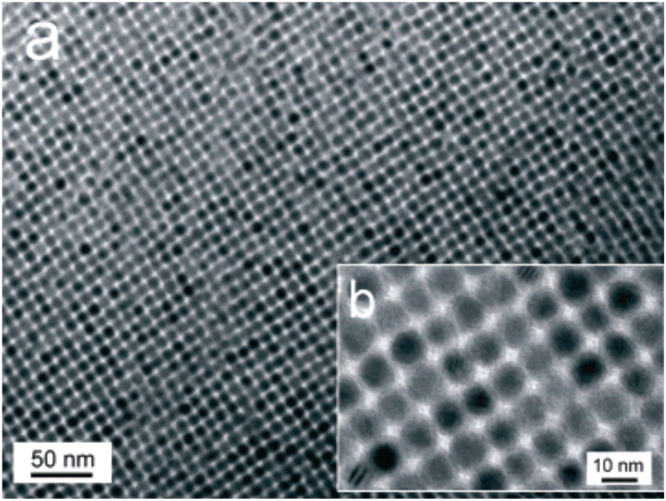
TEM images of as-synthesized SnTe NCs (10.2 nm) capped with oleic acid, (a) bar indicates 50 nm, (b) bar represents 10 nm. (Reproduced with permission from American Chemical Society 137 ).
Bis(3-mercapto-1-propanethiolato)tin(II), [Sn(SCH2CH2CH2SH)2] has been employed to grow thin films of orthorhombic SnS in the temperature range 300–400 °C on glass substrates. 103 Films could be deposited in the absence of H2S gas, unlike tin(IV) precursors, Sn(SR)4 which required H2S as an additional sulfur source (see later). The SnS films showed an optical band gap of ∼1.31 eV. Tin(II) aminothiolate complexes, [Sn{(SCH2CH2)2NR}] (R = Me or Et) (1) (Scheme 4) 87 and [Sn{SC(Me2)CH2NMe2}2] (2) (Scheme 4) 104 undergo a single step decomposition to give SnS. Microwave-assisted solvothermal decomposition of [Sn{(SCH2CH2)2NMe}] in N-methyl-2-pyrrolidone gave flake-like nanocrystals of SnS while the thermolysis of [Sn{SC(Me2)CH2NMe2}2] in OLA at 270 °C afforded orthorhombic SnS nanocrystals. The complex [Sn{SC(Me2)CH2NMe2}2] has also been used for growing thick and well-faceted orthorhombic SnS thin films on SiO2 substrate at 300 °C. 104 Similarly, a toluene solution of tin(II) thioamidate, [Sn{SCPri)NR}2] (R = Pri or But) (3) (Scheme 4) has been used for growing SnS thin films on SiO2-coated glass substrate in the temperature range 200–400 °C. 105 Another precursor, tin(II)thio-ureido (4) (Scheme 4) has been used for selective deposition of orthorhombic (α-SnS) and cubic zinc blende SnS (π-SnS) films of ∼800 nm thickness on glass substrates by AACVD. 106 The TG analysis revealed a single step decomposition with an onset temperature of ∼270 °C. The cubic phase SnS films were formed at 300 °C whereas orthorhombic SnS films were produced at higher temperatures (350–450 °C). These films showed optical band gaps of 1.78 and 1.34 eV(direct), respectively. 106 The photoelectrochemical analysis revealed that α-SnS films exhibited cathodic photocurrent (p-type behaviour) while π-SnS films showed both p- and n-type photocurrent behaviour. Mishra and coworkers synthesized a mononuclear tin(II) thiolate, [Sn(SBut)(tfb-dmeda)] by the reaction of [Sn(SBut)2] with Htfb-dmeda which undergoes decomposition in a single step in the temperature range 250–275 °C. 107 Using this precursor, films of various thickness (80 nm – 2 μm) of orthorhombic SnS have been deposited on different supports, like FTO, Mo-coated soda lime glass, in the temperature range of 330–450 °C by CVD method. 107

Structures of tin(II)precursors used for the synthesis of tin chalcogenides.
Tin(II) 1,1′-dithiolate/-diselenolate complexes have been used successfully as single source molecular precursors for the synthesis of tin chalcogenides. 108 , 109 , 110 , 111 The dithiocarbamate complexes, [Sn(S2CNRR’)2] (R/R’ = Et/Et, Me/Bun, Et/Bun) undergo thermal decomposition in the temperature range 210–360 °C yielding SnS. 109 , 110 However, in coordinating solvents decomposition of [Sn(S2CNEt2)2] takes place at much lower temperatures. In hexadecyl amine or oleyl amine the complex decomposes at temperature as low as 85 °C yielding nanocrystals of orthorhombic SnS. The shape and size of NCs can be modified by the solvent, duration and temperature of thermolysis. 110 Interestingly, 1,10-phenanthroline adduct, [Sn(S2CNEt2)2(phen)], on the other hand can be employed for the preparation of two different tin sulfides, viz. SnS and SnS2 by subtle variation in reaction parameters. 111 Thermolysis in a mixture of OLA and ODE (1:1 ratio) at 300 °C yields nanosheets (7 μm × 3 μm × 20 nm) of orthorhombic SnS which exhibits electrochemical properties with capacity of 350 mAhg−1 around 1.2 V. However, thermolysis at 280 °C in a mixture of OLA–OA- ODE (1:1:2 ratio) affords nanoplates (6 × 150 nm) of hexagonal SnS2. 111 A 1,1′-diselenolato complex, [Sn(Se2PPh2)2] has been successfully employed for orthorhombic SnSe films deposition on borosilicate glass plates at 400 °C under a flowing argon atmosphere by AACVD method. 108
3.1.2 Tin(IV) precursors for the synthesis of tin chalcogenides
Different classes of both classical and organotin(IV) chalcogenolates have been used for the synthesis of tin chalcogenides. Homoleptic tin chalcogenolates, viz., [Sn(SCH2CF3)4], 112 [Sn(SPh)4], 113 [Sn(SCH2CH2S)2], 114 [Sn(SePh)4] 115 and [Sn(Sepy)4], 97 on pyrolysis yield SnE or SnE2 depending on the nature of the precursor. The thiolate complexes, [Sn(SR)4] (R = CH2CF3, Ph) and [Sn(SCH2CH2S)2] require H2S as an additional source and yield different tin sulfides depending on the decomposition temperatures. 112 , 113 , 114 The complexes [Sn(SR)4] give SnS2 at 300–450 °C and SnS at 500–600 °C 112 , 113 whereas [Sn(SCH2CH2S)2] at 350, 400 and 500 °C produces yellow SnS2 (spherical particles of diameter 300 nm), brown Sn2S3 (needle like growth) and silver-grey SnS (overlapping plates of 2 × 2 µm), respectively thin films on glass substrates under AACVD conditions. 114 Penta- and hexa-coordinated tin(IV) selenolate complexes, [SnCl2{(SeCH2CH2)2NMe}] and [Sn{(SeCH2CH2)2NMe}2], respectively decompose in four steps to result in the formation of orthorhombic SnSe via SnSe2 intermediate generated at lower temperatures. The bis complex either on thermolysis at 350 °C or on microwave-assisted thermolysis in N-methyl-2-pyrrolidone at 300 °C yields hexagonal plates of diameter ranging from 7.5 to 20 μm of SnSe2. 116
Pyrolysis of [Sn(Sepy)4] in a sealed tube at 300 °C gives SnSe2 and py2Se, 97 whereas [Sn(SePh)4] on thermolysis at 300 °C produced NCs of SnSe. 115 Similarly bis(chalcogenolates), [Sn(EPh)2{N(SiMe3)2}2], obtained by oxidative addition of Ph2E2 on stannylene, [Sn{N(SiMe3)2}2], undergo single step decomposition (TGA) and on thermolysis in OLA at 210 °C yields nanocrystals of SnE (E = S, Se, Te). The size of NCs is influenced by duration of thermolysis. 117 For instance, the size of SnSe nanocrystals can vary from 60–90 nm, 0.5–1.0 µm and 250–500 nm, respectively for 20, 40 and 120 min. Reid and coworkers examined a series of butyltin chalcogenolates, [Bun 3Sn(EBun)] (E = S, Se, Te) and [Bun 2Sn(SBun)2] as molecular precursors for growing thin films of SnE on silica plates by LPCVD techniques. 118 , 119 The complexes, [Bun 3Sn(EBun)] (E = Se, Te) and [Bun 2Sn(SBun)2] produced orthorhombic SnE (E = S or Se) and cubic SnTe films, but [Bun 3Sn(SBun)] gave sulfur deficient SnS films. Cubic SnTe films were found to be p-type semiconductor. Their temperature dependent thermoelectric performance revealed peak Seebeck coefficient of 78 µVK−1 and power factor of 8.3 µWK−2 cm−1 at 342 °C. 119
Authors’ group 120 , 121 , 122 , 123 , 124 , 125 , 126 , 127 , 128 , 129 has developed diorganotin(IV) complexes derived from N-heterocyclic chalcogen ligands (Scheme 5) as molecular precursors. The complexes have been examined by NMR spectroscopy and single crystal X-ray diffraction analyses. These complexes have been successfully used for the synthesis of phase pure tin chalcogenides (SnE and SnE2) either in NC form or for growing thin films without any requirement of additional chalcogen source.

N-Heterocyclic chalcogenolate ligands (E = S or Se).
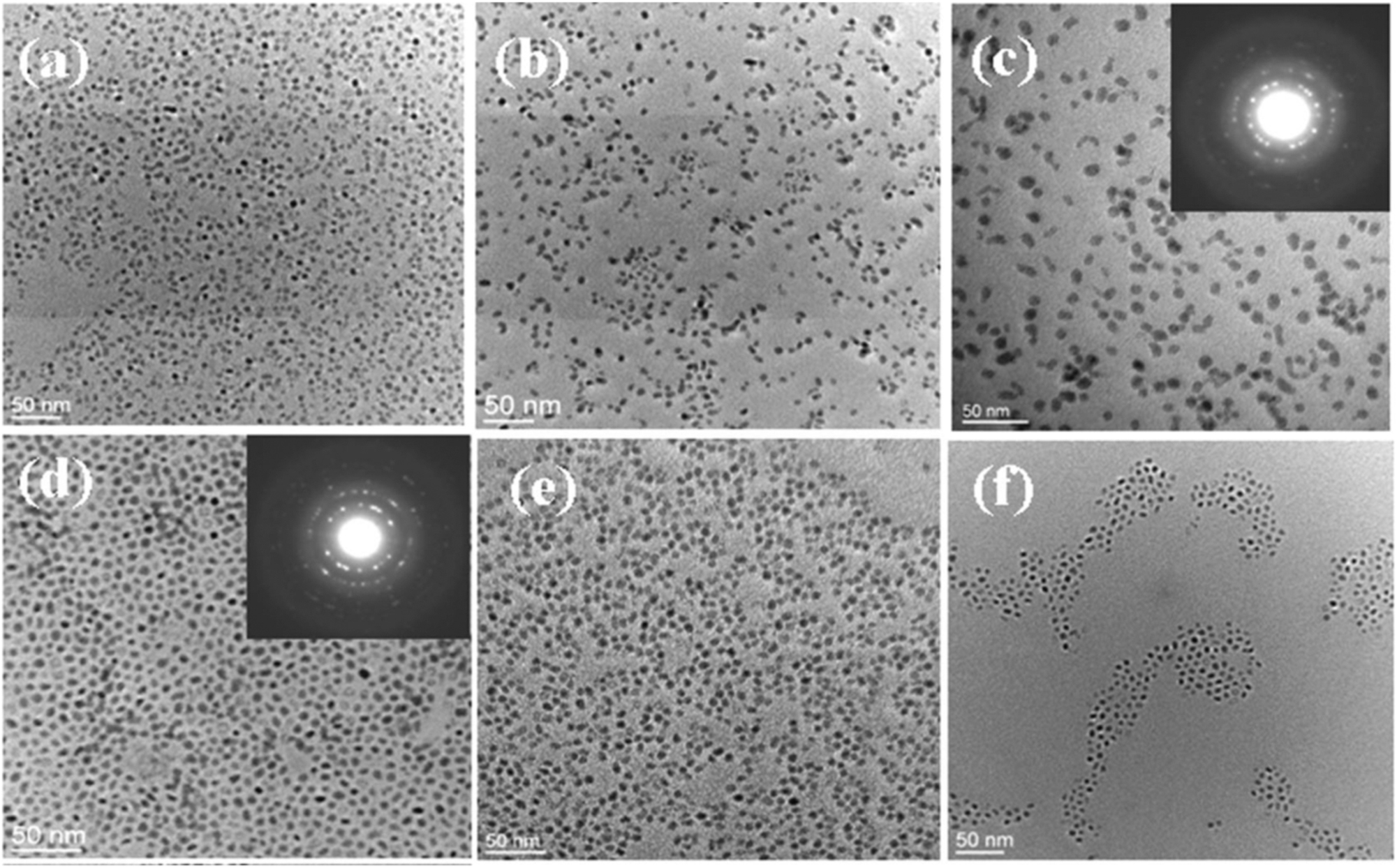
A number of diorganotin 2-pyridyl/2-pyrimidylthiolates, [R2Sn(Spy)2] (R = Me, Et, But), [R2Sn(Cl)(Spy)] (R = Et, But) and [R2Sn(Cl)(SpymMe2)] (R = Me, Et, But) on thermolysis through heat-up approach in OLA at 240 °C yields hexagonal nanosheets (thickness of 30–80 nm) (e.g. from Et2Sn(Spy)2]) and rectangular sheets (301 × 390 × 58 nm) (e.g. from [Et2Sn(Cl)(SpymMe2)]) of orthorhombic SnS with direct band gap of 1.61–1.90 eV. 124 , 129 Morphology and crystallite size of nanosheets of SnS produced from [But 2Sn(SpymMe2)2] in high boiling coordinating solvents (oleyl amine, octadecene, dodecane thiol), can be controlled by the reaction solvent. 122 For instance, SEM and TEM images of SnS prepared in OAm (Figure 7a and b) depicts rectangular nanosheets while those produced in DDT reveal a mixture of rectangular and hexagonal sheets (Figure 7d and e). On contrary, SnS obtained in ODE exhibit irregular nanosheets (Figure 7g and h). The interplanar spacing depicted in the respective HRTEM images point to orthorhombic SnS (Figure 7c, f and i). The thickness of these SnS nanosheets vary depending on the precursor employed in the thermolysis. For instance, the thickness of SnS nanosheets was around 50 nm in the case of [tBu2Sn(Spy)2] while dimensions of nanoplatelets obtained by thermolysis of [tBu2SnCl(Spy)] is larger due to relatively faster growth kinetics of nanoplatelet formation. 129 These precursors have also been utilized for the deposition of orthorhombic SnS thin films on glass and silicon substrates at 400 °C through AACVD. Microscopic images unveiled randomly oriented rectangular blocks and hierarchical flowers on the glass and silicon substrates. The morphological difference of SnS with respect to nature of the substrate has been ascribed to the orientation and interaction of the substrate atoms with the droplets of the precursor approaching the substrate surface. 124 Similarly, thermolysis of [tBu2Sn(Spyz)2] (HSpyz = 2-pyrazinyl thiol) in OLA at 300 °C gave rectangular sheets (size ∼30 nm) of orthorhombic SnS. 128
![Figure 7:
SEM, TEM and HRTEM images of orthorhombic SnS nanostructures synthesized by the thermolysis of [tBu2Sn(SpymMe2)2] at 250 °C for 10 min in (a–c) OAm, (d–f) DDT and (g–i) ODE, respectively (Reproduced with permission from Elsevier
122
).](/document/doi/10.1515/revic-2024-0141/asset/graphic/j_revic-2024-0141_fig_007.jpg)
SEM, TEM and HRTEM images of orthorhombic SnS nanostructures synthesized by the thermolysis of [tBu2Sn(SpymMe2)2] at 250 °C for 10 min in (a–c) OAm, (d–f) DDT and (g–i) ODE, respectively (Reproduced with permission from Elsevier 122 ).
Diorganotin 2-pyridyl, 3-methyl-2-pyridyl and 5-methyl-2-pyridyl, 4,6-dimethyl-2-pyridyl and 4,6-dimethyl-2-pyrimidyl selenolates undergo clean thermolysis in OLA to give different morphologies of orthorhombic SnSe (e.g. from [Me2Sn(Sepy)2], [Me2Sn(SepyMe2)2]) or hexagonal SnSe2 (e.g. from [R2Sn(SepymMe2)2]) nanoparticles depending on the nature of precursor. 121 , 123 , 125 , 126 For example, different nanostructures of tin selenide can be prepared by [tBu2Sn{SeC5H3(Me-5)N}2] on injecting in different solvent systems (ODE, OLA, OA or in 1:1 (v/v) ODE:OLA and OA:OLA). 126 Thermolysis of [tBu2Sn{SeC5H3(Me-5)N}2] in ODE and OLA yield hexagonal sheets of hexagonal phase SnSe2 and irregular sheets of orthorhombic SnSe (average thickness 18 and 12 nm), respectively. While in OA and in solvent mixtures (ODE:OLA and OA:OLA), a mixture of sheets of different shapes could be obtained. The nanoflakes of thickness as tiny as 10 nm are formed in OA:OLA mixture which has been attributed due to stronger binding of the oleate group. The complex, [Bu2 tSn(Sepy)2] has been employed to deposit films of orthorhombic SnSe on glass and p-type silicon(100) substrates at substrate temperature 490 °C. Similarly photo-responsive nanosheets of SnSe2 can be deposited from [Bu2 tSn(SepyMe-5)2]. 126 The complex [Bu2 tSn(SepymMe2)2] has been engaged to coat SnSe2 thin films on silicon wafers at 375 °C by AACVD. The direct band gaps of as deposited and annealed thin films are 2.12 and 2.06 eV, respectively. 125 The optical band gaps (direct band gaps for SnSe 1.68–1.78 eV 121 and for SnSe2 1.76–2.30 eV 125 ) of these nanostructures are blue shifted with reference to bulk material indicative of quantum confinement.
1,1′-Dithiolate complexes of tin(IV) are yet another family of precursors employed for the synthesis of tin sulfide NCs and for thin films deposition. 130 , 131 , 132 , 133 , 134 Heteroleptic dithiocarbamates, [Sn(SR)2(S2CNEt2)2] (R = CH2CF3, c-Hex) on heating undergo reductive elimination of disulfide (R2S2) with concomitant formation of tin(II) complex, [Sn(S2CNEt2)2] which after subsequent loss of (Et2NCS)2S yields SnS. 131 In contrast, tetrakis derivative, [Sn(S2CNEt2)4] takes a different decomposition path. 131 The complex starts decomposing either on leaving in CHCl3/CH2Cl2 at RT or on heating at 200 °C to a dimeric sulfido-bridged complex, [Sn(µ-S)(S2CNEt2)2]2, which on further heating to 375 °C leads to the formation of hexagonal SnS2. 131 Organotin dithiocarbamates, [Me3Sn(S2CNMeBun)] and [BunSn(S2CNMeBun)3], on the other hand, requires H2S as additional sulfur source when used for growing thin films of SnS. 132 In the absence of H2S gas no films could be grown. 132 In contrast, dibutyltin dithiocarbamates, [Bu2Sn(S2CNRR’)2] (R/R’ = Et/Et; Me/Bun; Bun/Bun; Me/n-Hex), in the absence of H2S gas, could produce orthorhombic SnS films on glass substrate in the temperature range 400–530 °C by AACVD method. 134 The films consisted of sheet-like crystallites and the presence of a small amount of SnO2. The nature of precursor and deposition temperature greatly influenced the band gap of the films which varied in the range 1.21–1.71 eV and the photo-sensitivity varied from 0.4 to 2.1 % for films deposited at 500 °C. 134 Thermolysis of dibutyltin bis(piperidine dithiocarbamate), [Bu2Sn{S2CN(CH2)5}2] in OLA at 230 °C yields nanosheets (998 × 465 nm) of phase pure orthorhombic SnS. 133 Like dibutyltin dithiocabamates, diphenyltin xanthates, [Ph2Sn(S2COR)2] (R = CH2CH2OMe, Bui) behave similarly. 130 SnS films deposited using these precursors on glass substrates in 400–575 °C range by AACVD were contaminated with some SnO2. 130 Thio-/seleno-benzoate complexes, [Bu2Sn(ECOPh)2] (E = S or Se) have been used for the preparation of orthorhombic SnE. 135 , 136 OLA capped nanosheets of SnSe have been prepared by hot injection method by injecting TOP dispersion of selenobenzoate complex to preheated OLA at 200 °C. Thin films of SnSe could also be grown on a glass substrate using a THF solution of the complex by AACVD. Uniform deposition of crystalline films takes place in the temperature range 375–475 °C. 135
Organotin chalcogenides have also been investigated as SSMPs for tin chalcogenides. Boudjouk and coworkers employed diorganotin chalcogenides, [(R2SnE)3] (R = Ph or Bz; E = S or Se) 94 , 137 and bis(triorganotin) chalcogenides, (R3Sn)2E (R = Ph or Bz; E = S, Se, Te) 94 , 138 as molecular precursors for the synthesis of SnE. Pyrolysis of [(R2SnE)3] under an inert atmosphere yields NCs of phase pure orthorhombic SnE (E = S or Se). 94 , 137 Pyrolysis of (Ph3Sn)2E under flowing nitrogen in a tube furnace at above 330 °C yields a dark grey powder of micro-crystalline orthorhombic phase of SnE (E = S or Se) and cubic SnTe. 138 In contrast, the corresponding benzyltin derivatives, (Bz3Sn)2E (E = S or Se) yield SnE contaminated with some elemental tin. 94 Flow pyrolysis of structurally characterized dibenzyltin telluride, [(Bz2SnTe)3] at 200–275 °C affords phase pure cubic SnTe nanocrystals of size ∼1 µm. 139 Chalcogenido-bridged diorganotin complexes, [Sn(µ-E){CH(SiMe3)2}2]2 (E = S, Se, Te) (5) (Scheme 6), obtained by oxidative addition of chalcogen on tin(II) compound [Sn{CH(SiMe3)2}2], are thermally quite stable. 140 , 141 Only tellurido-bridged complexes undergo decomposition and could be used for growing SnTe films on gold seeding layers at 400 °C. 140 Similarly other tin(IV) chalcogenide complexes (6–8) (Scheme 6) were obtained by oxidative addition of chalcogen on tin(II) complexes. 86 , 104 , 142 The complexes 6 can also be prepared by salt metathesis reaction between [Sn{(N-c-Hex)2CNMe2}2Br2] and Li2E 86 which on thermolysis in OLA at 210 °C yields nanocrystals of SnE. 86

Some representative tin(IV) precursors used for the synthesis of tin chalcogenides.
Reid and coworkers employed Lewis acid-base adducts of the type trans-[SnCl4(ER2)2] (E = S or Se; R = Et or Bun) and cis-[SnCl4(RE∩ER)] (E = S or Se; RE∩ER = BunE(CH2)nEBun (n = 2 or 3); o-(MeECH2)2C6H4) for deposition of tin chalcogenide thin films of various thickness on different substrates (Si; SiO2; TiN) using LPCVD methods. 143 , 144 , 145 Depending on precursor and decomposition temperatures, films of different tin chalcogenides could be grown. Complexes with chelating ligands decompose at higher temperatures with respect to those containing monodentate ligands. 144 , 145 In general, at lower deposition temperatures SnE2 is preferentially formed whereas at higher temperatures films of SnE are formed. For instance, cis-[SnCl4(BunE(CH2)3EBun)] at 286 and 480–500 °C gave SnS2 and SnSe2, respectively, but at 558 and 588 °C produced SnS and SnSe. 144 Boscher et al. instead of Lewis acid-base adducts, employed dual source – SnCl4 and Et2Se for growing thin films of SnSe and SnSe2 on glass substrate under LPCVD conditions. 146 SnSe films (100 nm thick) could be deposited at 650 °C whereas SnSe2 films of 10–80 μm size adherent crystals were formed at 600-650 °C. 146 Similarly, the dual source approach using SnCl4 and H2S, has been used to deposit different tin sulfides depending on the deposition temperatures. Thus, films of hexagonal SnS2, orthorhombic Sn2S3 mixed with some SnS2 and orthorhombic SnS could be deposited on glass substrate by APCVD method at 500, 525 and 545 °C, respectively. 147 The use of dual source precursors for growing thin films can be traced back to 1970s when Manasevit and Simpson deposited SnE (E = S, Se, Te) films on various substrates using tetramethyl tin and H2S/H2Se/Me2Te under a flow of hydrogen at 550, 500 and 650 °C, respectively. 148 Besides chalcogeno ether adducts, adducts of other chalcogen ligands, like thiosemicarbazone (e.g., [Bz3Sn(Cl){S=C(NH2)NH–N(=CHAr)}], where Ar = 2-HOC6H4; 4-ClC6H4), 149 N,N-dimethyl selenourea (e.g., [SnCl4{Se=C(NMe2)NH2}2]), 87 have also been explored as templates for tin chalcogenides. The selenourea complex, [SnCl4{Se=C(NMe2)NH2}2] undergoes a two-step decomposition. It yields SnSe2 at 400 °C (from TGA), but thermolysis either in OA or in an OA-OLA mixture at 350 °C produces nano-flakes of a mixture of SnSe and SnSe2. 87
3.2 Synthesis of ternary tin chalcogenides
Three different families of ternary tin chalcogenide materials, viz. anion- and cation-alloyed IV-VI materials (SnExE’y and Sn1-x-IVx-E) and MxSnyEz, can readily be identified, the latter being the most extensively studied semiconductors.
3.2.1 SnExE’y materials
The optical band gap and thermal conductivity of binary tin chalcogenides can be further fine-tuned in anion-alloyed ternary systems for their thin-film based solar-cell and thermoelectric applications. These materials can be generated by direct heating of stoichiometric quantities of constituent elements, 150 by heat-up method 151 or by molecular precursor route. 94 , 152 , 153
Organotin chalcogen compounds have been effectively probed as precursors for the synthesis of anion-alloyed materials. Pyrolysis of a mixture of [Bz2SnS]3 and [Bz2SnSe]3 in different molar ratios at 450 °C afforded ternary tin chalcogenides, SnS0·75Se0.25, SnS0·5Se0.5 and SnS0·25Se0.75, respectively as plate-shaped (∼4 μm) NCs. 94 The entire range of SnS1−xSex has been prepared by thermolysis of bis(thiobenzoato)dibutyltin(IV) and bis(selenobenzoato)dibutyltin(IV) in an appropriate molar ratios in OLA at 230 °C. A steady variation in the band gap on going from SnS (1.48 eV) to SnSe (1.1 eV) has been observed as revealed by UV-Vis-NIR analysis. 136
Oxidative addition of chalcogen on organotin(II) chalcogenides, (RSn)2X yields (RSnE)2X (R = 2,6-(Me2NCH2)2C6H3 −; X = S, Se and E = S, Se, Te) (Scheme 7) 152 , 153 which serve as a single source precursors for ternary tin selenides. These compounds contain two terminal Sn = E bonds 153 and decompose in multiple steps to give tin chalcogenides. Thermolysis of (RSnSe)2S yields SnS0·5Se0.5 whereas (RSnTe)2X (X = S or Se) gives only SnTe as the main product. However, SnSexTe1-x (x = 0–0.15) has been prepared by heating pure elemental Sn, Se and Te in stoichiometric amounts in a sealed quartz tube at 900 °C. 150

Oxidative addition of chalcogen on organotin(II) complexes.
The band gap of SnSxSe1-x nanocrystals (7–15 nm), obtained by hot injection method employing an ODE–OA solution of SnO treated with the solutions of TOP/Se and OLA/S at 270 °C, can be tuned from 0.92 to 1.24 eV with a linear change of S/(S + Se) and fall within the range of band gaps of SnS (1.6 eV) and SnSe (1.1 eV). 154 The band gap energy can effectively be modulated in a wide range of 0.96–2.26 eV in SnSxSe1-x, Sn(SxSe1-x)2, and Sn2S3 NCs (Figure 8). 155 Thin films of semiconducting SnSSe material have been deposited by spin-coating methods at varying spinning speeds. For instance, amorphous films of Sn42S41Se17 with an optical band gap of 1.79 eV are deposited at 1,500 rpm. 153 Thin films deposited using a hydrazine solution of SnS2, SnSe2 and sulfur followed by annealing at 270 °C had the composition SnS2-xSeX. 151 These films exhibited n-type transport properties with large current densities greater than 105 A cm−2 and mobilities higher than 10 cm2 V−1 s−1.
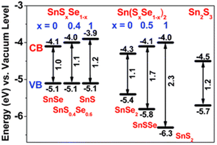
Schematic representation of band gap energy of SnSxSe1-x, Sn(SxSe1-x)2, and Sn2S3 NCs (reproduced with permission from Royal Society of Chemistry 155 ).
3.2.2 Sn1-x-IVx-E materials
A number of cation-alloyed ternary IV–VI group semiconductors have been synthesized by several methods. Earlier methods relied on direct heating of stoichiometric quantities of constituent elements in sealed ampules (such as SnxGe1-xSe (0 ≤ x ≤ 1)) at high temperatures, 156 but the current methods employ solution techniques. Nanocrystals of SnxGe1-xSe (0 ≤ x ≤ 1) have been prepared by injecting a hexamethyldisilazane solution of But 2Se2 into hot (95 °C) dodecyl amine solution of GeI4 and SnI4 mixture in a desired ratio and heating further at 225 °C. 157 Powder X-ray diffraction patterns of SnxGe1-xSe (0 ≤ x ≤ 1) point out orthorhombic Pmna crystal structure for these nanocrystals (Figure 9). The indirect band gap energy of these NCs varied in the range 0.87–1.13 eV as a function of x = 1.0–0.2. Nanosheets of SnGeS3 have been isolated by thermolysis of xanthate complexes, [M(S2COPri)4] (M = Ge and Sn). These photo-responsive nanosheets exhibit a band gap of 1.59 eV as measured from diffuse reflectance spectroscopy (DRS). 158
XRD patterns of SnxGe1−xSe nanocrystals with different compositions. (Reproduced with permission from American Chemical Society 157 ).
Ternary Pb1-xSnxE compounds are narrow band gap semiconductor materials. They exist in a cubic rock salt crystal structure. Nanocrystals of Pb1-xSnxS (av. size 8 nm) have been isolated by solvothermal route. In this method an OLA solution of sulfur is swiftly added to a hot solution of a mixture of stannous oxide and lead oxide in ODE and OA and heated further at 270 °C. The band gap (1.57 (when x = 0.54) to 1.96 eV (when x = 0.85)) varied nearly linearly with the gradual rise of Pb/(Pb + Sn) ratio. 159 A series of Pb1-xSnxTe nanocrystals (∼7.5 nm in size) have been synthesized by the reaction of lead oleate and [(Me3Si)2N]2Sn mixture with a TOP solution of tellurium at 150 °C. These NCs unveil band gaps in the mid-IR region. TEM images of the pristine Pb1-xSnxTe NCs are nearly spherical with the average particle size varying between 6.0 and 8.7 nm irrespective of all compositions (Figure 10). Here, Pb0·86Sn0·14Te and Pb0·14Sn0·86Te NCs are monodispersed and spherical in shape while the morphology of Pb0·5Sn0·5Te NCs varies from spherical to oval and are polydispersed in nature. The change in morphology of NCs has been attributed due to the different binding affinity of Pb and Sn precursors with oleic acid and amine moieties. 160
TEM images of the (a) Pb0·86Sn0·14Te, (b) Pb0·8Sn0·2Te, (c) Pb0·5Sn0·5Te, (d) Pb0·33Sn0·67Te, (e) Pb0·2Sn0·8Te and (f) Pb0·14Sn0·86Te NCs. (Reproduced with permission from American Chemical Society 160 ).
3.2.3 MxSnyEz materials
Various synthetic methods for the NCs of Cu2SnE3 (E = S, 56 , 161 , 162 , 163 Se 67 , 164 , 165 , 166 , 167 , 168 , 169 , 170 ) have been reported and include heat-up, hot-injection, solvothermal/hydrothermal routes. Reactions in these synthetic routes are carried out in different solvents, like OLA, ODE, OA, HDA, TOPO, using a range of copper (CuCl, CuI, CuCl2, Cu(acac)2) and tin (SnCl2, SnBr2, SnCl4, Sn(acac)2, Sn(OAc)2) precursors and a chalcogen source (S, Se, SeO2, DDT, thio-/seleno-urea, But 2Se2, Ph2Se2). 171 Several factors like metal precursor reactivity, nature of chalcogen source, reaction medium, and the reaction temperature, have a strong impact on the phase of the NCs. The use of different sulfur sources can give different phases. NCs of Cu2SnS3 synthesized by hot-injection route using an ODE solution of CuCl and SnCl2 on treatment with OLA solution of sulfur at 240 °C affords the zinc blende phase, whereas treatment with dibutyldithiocarbamic acid (DBDCA) in ODE with a suitable capping agent (DDT, TOPO, OA) results in the formation of wurtzite phase. 172 Formation of different phases of Cu2SnS3 NCs in the reaction of CuI, Sn(OAc)2 with DDT could be managed by proper selection of solvent. The use of ODE at 220 °C results in the formation of zinc blende phase whereas in OLA at 190 °C wurtzite phase of NCs is formed. 173
Hot injection method has been frequently used for the preparation of Cu2SnSe3 NCs. Wang et al. from the reaction of CuCl, SnCl2 in oleyl amine with Ph2Se2 at 310 °C isolated NCs of Cu2SnSe3 as tetrapods consisting of cubic core with four wurtzite arms. 67 , 170 Brutchey and co-workers 169 synthesized NCs (15.1 ± 2.9 nm) of wurtzite phase by treatment of a dodecyl amine-DDT solution of CuCl and SnI4 with di-tert-butyl-diselenide (But 2Se2). In these reactions, different phases could be conveniently controlled by suitable choice of capping agent and reaction temperatures. 169 , 170 Different crystal phases, cubic, zinc blende, hexagonal, wurtzite and monoclinic with varied morphologies of CTSe could be isolated by slight variation in the reaction parameters. 174 The wurtzite/monoclinic phase is typically formed at lower temperatures but on increasing the temperature the cubic phase is obtained. 174 , 175
Authors’ group employed organotin precursors for the synthesis of Cu2SnE3 (E = S or Se) (Figure 11). 127 , 128 Thermolysis of [But 2Sn(Spyz)2] and [Cu(Spyz)(PPh3)2] (HSpyz = 2-mercapto pyrazine) in 1:2 ratio in OLA at 300 °C yields nano-crystals (∼22 nm) of phase pure monoclinic Cu2SnS3. However, thermolysis either at lower temperatures or in a mixture of OLA-OA gave monoclinic CTS slightly contaminated with binary sulfides. 128 The band gaps of Cu2SnS3 nanostructures (1.4 eV) are blue shifted relative to bulk counterparts. Similarly, co-thermolysis of [Cu(SepyMe-3)]4 and [Me2Sn(SepyMe-3)2] in 1:2 M ratio in OLA or TOPO at 300 °C produced cubic Cu2SnSe3 nano-crystals (11 ± 1 nm). These NCs could be isolated in flower-shaped, dish-like, nano-sheets, polyhedra morphologies by subtle variation in the reaction conditions. For instance, SEM of Cu2SnSe3 isolated by hot injection of [Me2Sn(SepyMe-3)2] and [Cu(SepyMe-3)]4 in OLA at 300 °C revealed polyhedra shape of NCs (Figure 12). 127

![Figure 12:
SEM image of Cu2SnSe3 polyhedra obtained by hot injection of [Me2Sn(SepyMe-3)2] and [Cu(SepyMe-3)]4 in OLA at 300 °C. (Reproduced with permission from Springer Nature Publishers
127
).](/document/doi/10.1515/revic-2024-0141/asset/graphic/j_revic-2024-0141_fig_012.jpg)
SEM image of Cu2SnSe3 polyhedra obtained by hot injection of [Me2Sn(SepyMe-3)2] and [Cu(SepyMe-3)]4 in OLA at 300 °C. (Reproduced with permission from Springer Nature Publishers 127 ).
O’Brien and coworkers deposited thin films of cubic Cu2SnSe3 using a THF solution of Cu(acac)2 and [Sn(Se2PPh2)2] in 2:1 stoichiometric ratio by AACVD at 400 and 450 °C. Films grown at 400 °C consisted of nanocrystalline flakes of CTSe while those deposited at 450 °C consisted of semi-spherical crystallites. 108
Nanocrystals of Cu3SnS4 have been isolated by hot injection and solvothermal methods. Orthorhombic Cu3SnS4 NCs (31.8 ± 4.9 nm) and nanosheets (15 nm thick with a lateral dimension of 209 ± 33 nm) have been prepared by hot-injection route employing Cu(acac)2, SnCl4, followed by either seeding with monoclinic Cu31S16 NCs or by adding DDT. 177
ZnSnS3 is another interesting material. It exists in three closely related phases, viz. non-polar monoclinic and ilmenite and a polar lithium niobate (LN) form. The latter with a band gap of 1.28 eV exhibits ferroelectric behaviour. 178 Being a material with a narrow band gap, it is highly effective in countering the major limitation of traditional ferroelectric PV devices which employ oxide materials that have large band gaps (>3 eV). The films of LN-ZnSnS3 and LN-ZnSnS3@rGO have been prepared by hydrothermal method using ZnSn(OH)6 and thiourea. 179 , 180
The compound In4SnSe4 (band gap = 1.6 eV) is another narrow band gap ternary system. Nanowires (length 5–20 µm and width 100–400 nm) of In4SnSe4 have been prepared by heat-up method using SnCl2, InCl3, and Ph2Se2 in a mixture of ODE and OLA containing excess hexamethyldisilazane at 300 °C. 181
3.3 Synthesis of quaternary tin chalcogenides
The interest in quaternary materials, I2-II-IV-VI4 (I = Cu, Ag; II = Zn, Cd, Hg; IV = Si, Ge, Sn; and VI = S, Se, Te) gained momentum around 2007 due to their numerous technological applications. 171 , 182 These quaternary materials are derived from substitution of cations in binary II-VI materials which adopt two crystallographic structures, viz. zinc blende (ZB) and Wurtzite (WZ). The most widely investigated quaternary systems are Cu2ZnSnS4 (CZTS) and Cu2ZnSnSe4 (CZTSe), although various other materials like Cu2ZnSnTe4, Cu2CdSnS4, Cu2CdSnSe4, Cu2MSnS4 (M = Mn, Fe, Co, Ni) have also been studied. As the number of constituent elements increases, synthesis of compositionally pure and single phasic quaternary systems becomes as elusive as complex. In such cases selection of precursors, ligands, solvents and reaction parameters are of paramount importance in order to avoid the formation of binary/ternary phases.
3.3.1 Synthesis of Cu2ZnSnE4 (E = S or Se)
Although there are several synthetic approaches to prepare Cu2ZnSnS4 (CZTS), to isolate high-quality stoichiometric materials over a large area remains a challenging task. Synthetic strategies employed for the preparation of CZTS include hydrothermal/solvothermal, 183 , 184 hot-injection method, 60 , 66 , 185 , 186 heating-up method, ultrasound-assisted microwave, 187 etc., hot-injection method being the most common technique. In these synthetic methods stoichiometric quantities of metal salts of copper (CuCl2·2H2O, Cu(OAc)2.H2O, Cu(acac)2), zinc (ZnCl2, Zn(OAc)2.2H2O, Zn(acac)2) and tin (SnCl2·2H2O, SnCl4·5H2O, Sn(OAC)4) are dissolved in a suitable solvent (ethylene glycol, OLA, ODE, TOPO, monoethanolamine, etc.) and then treated with a sulfur source like elemental sulfur in OLA, thiourea, or thiols (DDT, tert-dodecane thiol). Alternatively, metal and the sulfur source can be substituted by metal complexes derived from sulfur ligands like diethyldithiocarbamate 1 , 188 , 189 , 190 , 191 and xanthates. 192 Diethyldithiocarbamate complexes, [Cu(S2CNEt2)2], [Zn(S2CNEt2)2] and [Sn(S2CNEt2)4] on thermolysis in oleyl amine/trioctyl amine have been successfully used to prepare NCs of CZTS. 1 , 190 , 191 Capping agents like OA, 1 , 193 hexadecane thiol, 190 are quite often employed to stabilize the NCs. For instance, Lu et al. generated wurtzite CZTS nano-prisms of size of 20 × 28 nm and nanoplates of thickness 14 nm in DDT/OLA and DDT/OA, respectively (Figure 13). Nanostructured thin films of CZTS have been grown by air spraying a THF solution of Cu(S2CNEt2)2, [Zn(S2CNEt2)2] and [Sn(tBu)2(S2CNEt2)2] in 2: 1: 1 M ratio on a heated (450 °C) glass substrate under an argon atmosphere. 188 Similarly, CZTS thin films have been deposited by AACVD on a glass substrate using a toluene solution of Cu(S2CNEt2)2, [Zn(S2CNEt2)2] and [Bu2Sn(S2CNEt2)2] in 2: 1: 1 M ratio. 189 Thin films of CZTS were grown on a glass substrate by spin coating technique using a THF solution of [(Ph3P)2Cu(S2COEt)], [Zn(S2COnBu)2] and [Sn(S2COEt)2] in 2: 1: 1 M ratio and finally heating in a furnace at an appropriate temperature. The films annealed at temperatures <375 °C produced hexagonal phase whereas annealing between 375 and 475 °C produced tetragonal material. 192 Copper zinc tin selenide (Cu2ZnSnSe4 (CZTSe) has also been prepared by different methods. Hot-injection route using metal salts in an amine (e.g., HDA) and trioctylphosphine selenide (TOPSe) was first reported. 194 Polycrystalline NCs of size 25–30 nm of CZTSe have been prepared by hot-injection method at 280 °C employing CuCl2, ZnCl2, SnCl4 and (Et3Si)2Se in ODE and OA mixture. 195 The samples prepared by different routes generally show compositional inhomogeneities. 171 Fuhrmann and coworkers synthesized Cu2ZnSnE4 by co-thermolysis of [(tmeda)Zn(µ-E)2{(SnR2)2E}] (R = Me, But or Ph; E = S or Se) with [{(Pri 3P)Cu}2(ECH2CH2E)]. 196
TEM images of wurtzite CZTS a) nano-prisms and b) nanoplates prepared in DDT/OLA and DDT/OA, respectively (reproduced with permission from Royal Society of Chemistry 193 ).
Depending on reaction temperature and the nature of sulfur source, different crystallographic forms can be isolated 197 , 198 whereas solvent can contribute to the final shape of CZTS nanoparticles. 199 The reaction between metal salts and sulfur powder in an appropriate solvent at high temperatures generally yields nanocrystals of kesterite CZTS. 195 Owing to strong coordinating ability, thiols as a sulfur source, on the other hand, allow the isolation of metastable phases. Thus, the reaction between metal salts and alkanethiols, such as DDT 186 , 193 or even the thermolysis of metal dithiocarbamate complexes in the presence of thiols (hexadecane thiol) 190 results in the creation of wurtzite CZTS. Thiols also serve as an effective passivating agent for the wurtzite facets and help in decreasing the overall size of the NCs. Another metastable phase–orthorhombic CZTS, could be prepared via hydrothermal method employing stoichiometric quantities of metal chlorides and thiocarbamide dissolved in a mixture of water-ethylenediamine, followed by heating at 200 °C. Orthorhombic CZTS undergoes phase transition on annealing at 500 °C to the tetragonal kesterite structure. 65 The films deposited by thermal degradation of spin-coated CZTS nanoparticles ink gave different CZTS phases depending on the annealing temperature. Annealing at 200 °C produced a mixture of cubic and hexagonal phases, at 350 °C only cubic CZTS phase was formed, while at 500 °C the tetragonal kesterite structure existed. 66
3.3.2 Synthesis of Cu2MSnS4 (M = Mn, Fe, Co, Ni)
There are several protocols to prepare nanocrystals of first-row transition metal ions incorporated compounds, Cu2MSnS4 (M = Mn, Fe, Co, Ni). These include hydrothermal/solvothermal, 200 , 201 , 202 , 203 hot injection, 204 spray pyrolysis, 205 direct spin-coating or spin-coating of nanoparticles/sol–gel, 206 , 207 , 208 , 209 electrodeposition, 210 etc. In these preparative methods stoichiometric quantities of metal salts of copper (CuCl, CuCl2·2H2O, Cu(NO3)2·6H2O, Cu(OAc)2.H2O, Cu(acac)2), tin (SnCl2·2H2O, SnCl4·5H2O) and transition metal salts (MnCl2·4H2O, Mn(OAc)2.4H2O/FeCl3·6H2O, FeSO4·7H2O, Fe(acac)2/CoCl2·6H2O/NiCl2·2H2O, Ni(NO3)2·6H2O) either as an aqueous solution or in an organic solvent (2-methoxy ethanol, OLA, or organic acids like acetic/citric acid) is treated with a sulfur source like thiourea, Na2S, Na2S2O3·5H2O, elemental sulfur in OLA. Quite often traces of secondary phases (binary and ternary) are also formed. Cui et al. 211 described a general solvothermal method in which a hexylamine solution of CuCl, SnCl2 and MCl2/(NO3)2 is treated with a mixture of carbon disulfide and 3-mercaptopropionic acid, followed by heating in an autoclave. The method is employed for the preparation of nanocrystals of these compounds in both zinc blende and wurtzite phases. 211
Tuneable crystal phases can be prepared by subtle variation in the reaction conditions. 212 , 213 NCs with the stannite structure of Cu2CoSnS4 (band gap 1.58 eV) have been prepared by solvothermal methods, 214 , 215 while the wurtzite structure could be synthesised by a hot-injection route. 216 On annealing the NCs of wurtzite phase at 400 °C led to the conversion in pure stannite structure. The structure of Cu2MSnS4 can also be modified by employing a suitable sulfur source in the reaction. For instance, the use of thiourea as a sulfur source in hydrothermal synthesis of Cu2MnSnS4 results in the formation of microspheres of a mixture of hexagonal and tetragonal forms, whereas use of Na2S in place of thiourea in the reaction afforded fine crystallites of tetragonal phase. 217
Transition metal incorporated ternary materials show magnetic behaviour. Nanocrystals of Cu2MnSnS4 and Cu2NiSnS4 display superparamagnetic behaviour at low temperature, whereas NCs of Cu2FeSnS4 and Cu2CoSnS4 exhibit ferromagnetic behaviour. 211 Cu2MnSnS4 (band gap 1.1 eV) shows feeble ferromagnetic behaviour at 2 K. 218
4 Applications of tin chalcogenides
Binary tin chalcogenides in general find wide array of applications in solar cells, thermoelectric devices, anode material for lithium-ion batteries, etc. due to attributes like suitable band gap range, high optical absorption coefficient (>104 cm−1), anharmonicity. 78 , 83 , 219 The effectiveness of these applications is further enhanced in 2D layered tin chalcogenides. The basic structure of single-layer tin chalcogenides (SnE) is distinctly different from other layered metal chalcogenides and comprises armchair and zig-zag arrangement of tin and chalcogen atoms (Figure 14). 219 , 220

In general application of a semiconducting material depends on its physicochemical, optical and electronic properties as well as size, shape, composition, crystal and band structures, etc. which in turn is governed by synthetic routes and post-synthetic surface modifications. Among various synthetic approaches described earlier, exfoliation of material in top-down approach can be utilized for the preparation of 2D layered materials which can be used for thermoelectric devices while the 2D nanostructured thin films deposited by using SSMPs can be utilized for photovoltaic applications. The bottom-up approach relying on solution phase/colloidal synthesis of nanomaterials provides a good control over the morphology (0D, 1D, 2D and 3D, etc.), phase and composition. Accordingly, these materials can be employed for different applications. For instance, 0D materials, especially quantum dots (QDs) are preferable for bio-imaging 221 and dye degradation 222 while 1D nanowires, nanorods are better choice for field effect transistor (FET), 78 , 223 sensors 78 and photovoltaic, 224 etc. applications. Solvothermal synthesized 1D SnS nano-rods show outstanding emission properties viz. low turn-on field (2.5 V/μm for 10 μA/cm2), high emission current density (647 μA/cm2 at 3.9 V/μm) and superior current stability (5 h for ∼ 1 µA). 223 On the other hand, 2D materials where the charge carriers are quantum confined along their thickness and having a large dielectric contrast produce large exciton binding energies leading to exceptional optical and electronic properties.
4.1 Photovoltaic solar cells
Silicon-based solar cells currently command photovoltaic energy generation with ∼95 % market share (https://www.energy.gov>eere>solar-photovotaic-cell). To overcome the inherent drawbacks of silicon, thin film-based PV devices fabricated from direct band semiconductor materials like CdTe, CuInE2 (E = S or Se) gained traction. 225 Scarce abundance of In, Te and toxicity of cadmium, however, limit their large-scale PV utilization. Tin chalcogenides (binary, ternary, quaternary materials) are well-suited for PV applications 39 , 53 as they fulfil the following criteria expected from an ideal material for PV applications. 226
Direct-band semiconductor with band-gap of 1.1–1.7 eV.
High photovoltaic conversion efficiency.
Easily accessible constituent elements with low or nearly no toxicity.
Binary tin chalcogenides SnS and SnSe have an ideal bandgap energy (∼1.3 eV), high absorbance coefficient (>10−4 and >10−5 cm−1) and high carrier concentrations (1015–1018 cm−3) making them promising candidates as absorber material for PV solar cells. Their thin layers (∼300 nm thick) can absorb most of the useful solar spectrum. Theoretically predicted maximum power conversion efficiency (PCE) is 32 % for SnE-based single junction thin film solar cells. 227 A number of groups have fabricated PV devices based on SnE thin films deposited by a variety of methods and reported PCE of 0.1–6.4 % depending on the structure of SnE and solar cell configuration. 83 , 228 , 229 Ahmet et al. fabricated solar cells using α-SnS and π-SnS thin films with two different configurations – Mo/SnS/CdS/i-ZnO/ITO and FTO/SnS/CdS/i-ZnO/ITO and demonstrated that the α-SnS based devices performed better with PCEs of 0.82 and 0.88 % than the π-SnS thin film-based devices with PCEs of 0.21 and 0.15 %, respectively. 228 Elongated anisotropic NCs (19.0 ± 5.1 nm) of orthorhombic SnSe, prepared from anhydrous SnCl2 and But 2Se2 in a mixture of dodecyl amine and dodecane thiol (5:1 v/v ratio) at 180 °C, exhibit photovoltaic properties. 224 The orthorhombic SnSe films, deposited from [Bu2 tSn(Sepy)2] on glass and p-type silicon(100) substrates at 490 °C, in Si/SnSe/Au configuration showed photo-response with a bias of 1.5 V. There was ̴20 % increase in the current under illumination conditions (Figure 15). 123 Similarly nanosheets of SnSe2, obtained from [Bu2 tSn(SepyMe-5)2], show photo response and the photocurrent increased under illumination. 126
![Figure 15:
Photo-response of the SnSe thin film deposited on a silicon substrate by the AACVD of [But
2Sn(Sepy)2] at 490 °C with a bias voltage of 1.5 V (reproduced from Royal Society of Chemistry.
123](/document/doi/10.1515/revic-2024-0141/asset/graphic/j_revic-2024-0141_fig_015.jpg)
Photo-response of the SnSe thin film deposited on a silicon substrate by the AACVD of [But 2Sn(Sepy)2] at 490 °C with a bias voltage of 1.5 V (reproduced from Royal Society of Chemistry. 123
Owing to the anisotropic structure, SnE (E = S or Se) show a reckonable difference in their optical and electrical properties along different crystallographic directions. For instance, electrical conductivity of SnS nano-sheets differ significantly in two different anisotropic crystalline directions. 230 The geometry-controlled SnE nanosheets have been projected for their high-efficiency photonics and electronics applications. 230 Furthermore, 2D nanosheets of SnS 231 and SnSe 232 have also been employed as absorbing layers of solar cells with photoelectric conversion efficiency of 1.45 and 4.8 %, respectively.
Ternary and quaternary compounds have also been investigated for their photovoltaic solar cell applications. Cu2SnS3 and Cu2SnSe3 are isostructural and their NCs have an attractive potential for making low-cost thin-film-based solar cells due to their solution processability. The status of CTS for solar cell applications has been reviewed. 233 , 234 A general schematic configuration of solar cells is illustrated in Figure 16. Tetragonal Cu2SnS3 thin-films based solar cells have been designed with graphite/Cu2SnS3/ZnO/ITO/SLG configuration. The cells showed PCE of 2.1 % with open circuit voltage. 235 Recently it has been shown that the solar cell constructed using NCs of wurtzite-CTS showed much better (13.1 % PCE) photovoltaic performance in comparison to the zinc blende phase (7.87 % PCE). 236
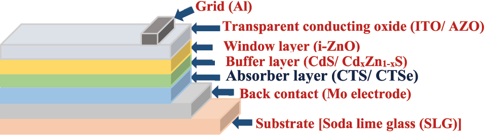
A general schematic configuration of Cu2SnE3 solar cells.
Nanostructures of Cu2SnE3 (E = S or Se), prepared by using organometallic precursors, exhibit photo response in a photo-electrochemical cell. 127 , 128 Photo-response of nanostructures (CTS, SnS and Cu1·8S) has been assessed. A nonlinear current voltage (I–V) behaviour of their nanostructures has been noted. CTS nanostructures exhibited better photosensitivity as well as increased photo-response over several on-off cycles with faster switching characteristics as compared to Cu1·8S particles. 128 The nano-structures of Cu2SnSe3 in a photo-electrochemical cell (Figure 17) exhibited a PCE of 1.7 %. 127
![Figure 17:
Current vs time plot of CTSe nanostructures obtained by thermolysis of [Me2Sn(2-SeC5H3(Me-3)N)2] and [Cu{SeC5H3(Me-3)N}]4 in OLA at 300 °C by heat up method showing switching behaviour under light intensity of 200 μW/cm2; b expanded view of one of the cycle. (Reproduced with permission from Springer Nature Publishers.
127](/document/doi/10.1515/revic-2024-0141/asset/graphic/j_revic-2024-0141_fig_017.jpg)
Current vs time plot of CTSe nanostructures obtained by thermolysis of [Me2Sn(2-SeC5H3(Me-3)N)2] and [Cu{SeC5H3(Me-3)N}]4 in OLA at 300 °C by heat up method showing switching behaviour under light intensity of 200 μW/cm2; b expanded view of one of the cycle. (Reproduced with permission from Springer Nature Publishers. 127
The energy band gap of CZTS (∼1.5 eV) exists in the visible region and can be further tuned by changing the composition, phase and size of the NCs. For example, the band gap of the wurtzite phase of Cu2ZnSn(S1-x,Sex)4 can gradually be tuned from 1.4 eV (for x = 0) to 0.9 eV (for x = 0.8) (Figure 18). 237 The CZTS band gap can be altered from 1.5 to 1.8 eV by reducing NCs size from 7 to 2 nm–a regime (∼3 nm) where quantum confinement effect can be noted. 1
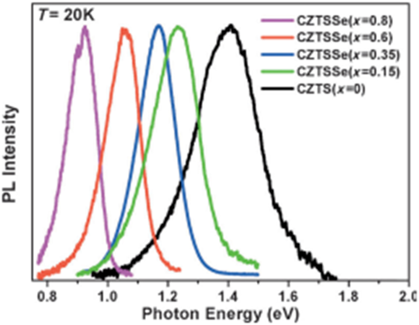
Photoluminescence (PL) emission of Cu2ZnSn(S1-x,Sex)4 nanocrystals. (Reproduced with permission from Wiley. 237
Tuneable band gaps lying in the visible region and excellent light absorption coefficients of these materials are apt for photovoltaic applications. The early investigations on CZTS-based solar cells reported 6.7 % photoelectric conversion efficiency 12 which with successive improvements in preparation of materials with different solar cell device structures 238 , 239 , 240 , 241 have reached ∼11 %. 241 Further improvement in photoelectric conversion efficiency (12.6 %) 242 is reported on selenization, Cu2ZnSn(SSe)4. There is a huge difference between the experimentally observed and theoretically predicted (31.6 %) PCEs. 227 A number of factors have been attributed for the large gap in power conversion efficiencies. These include structural defects in the CZTS absorber, presence of different phases, which is often the case, each having different electrical properties (Table 3), 192 presence of secondary materials.
Electrical properties of different phases of CZTS (data from 192 ).
| Hexagonal material (wurtzite phase) | Tetragonal (kesterite phase) | |
|---|---|---|
| Resistivity (Ω cm) | 27.1 | 1.23 |
| Carrier concentration (cm−3) | 2.65 × 10¹⁵ | 4.55 × 10¹⁷ |
| Hall mobility (μ) (cm2 V−1 s−1) | 87.1 | 11.1 |
| Hall coefficients (RH) (C−1 cm3) | 2.36 × 10³ | 13.7 |
| Conductivity (σ) (S cm−1) | 0.0369 | 0.81 |
Cu2MSnS4 (M = Mn, Fe, Co, Ni) based on earth-abundant elements have also been explored as an alternate material for low-cost solar cells. They are p-type direct-band semiconductor materials with an energy band gap of 1.21–1.69 eV and exhibit good photostability with desirable optical absorption coefficient (>104 cm−1). 206 , 207 , 208 , 209 , 210 Photovoltaic devices with Mo/Cu2MnSnS4/CdS/TCO/top and SLG/Cu2CoSnS4/Al geometry were fabricated and evaluated for their power conversion efficiencies. 209 , 210 The PCE of the former device was 0.19 % which increased to 0.73 % on sodium doping. 243 The SLG/Cu2CoSnS4/Al photodetector exhibited current amplification by an order of magnitude from dark to solar lamp and 1,064 nm IR laser illuminations. 209
4.2 Dye sensitized solar cells
Dye sensitized solar cells (DSSC) is another approach to utilize solar energy. A typical configuration of a DSSC is a transparent conductive glass substrate, a sensitizer adsorbed photoanode (usually TiO2 nanoparticles), platinum as a counter electrode (CE) which are placed in a redox electrolyte solution such as I−/I3 −, S2−/Sx 2−, etc. There have been sustained efforts to enhance the performance of DSSCs; replacement of platinum as CE is one of the strategies among various other components of the cell. 244 Numerous metal chalcogenides have been explored due to their rich intercalation chemistry and electronic properties.
Tin chalcogenides have also been explored as an absorber material in DSSCs. Binary chalcogenides, SnS2, SnSe2 and SnSe have been examined as counter electrodes in a DSSC. 245 , 246 , 247 Reduced graphene oxide composite of SnS2 nanoparticles (SnS2@rGO) as CE exhibited a PCE of 7.12 % in DSSC. The PCE of SnS2@rGO is comparable to platinum CE (6.79 %), but much better than either SnS2 nanoparticles (5.58 %) or graphene sheet alone (3.73 %). 247 Screen-printed SnSe and platinum counter electrodes exhibited PCEs of ∼5.76 % and 8.09 % with open-circuit voltages of 0.63 and 0.68 V, respectively in DSSC containing iodide/triiodide redox couple. 245 Hierarchical nano-structures (HNs) of SnSe and SnSe2 obtained in a solvothermal method has been used as counter electrodes in a dye sensitized solar cell which demonstrated photovoltaic performances similar to the device fabricated with a traditional platinum counter electrode. 246 A PCE of 5.60 % is realized when SnSe2 HNs were employed as the counter electrode of DSSC which is nearly equal to the efficiency noted for a conventional Pt counter electrode (5.74 %). SnSe2 QDs deposited on TiO2 nanocrystalline porous films show PCE of 0.12 % under AM 1.5, 1 sun, which is much higher than the bare TiO2 electrode (PCE = 0.004 %). 248
The photovoltaic properties of quaternary tin chalcogenides, besides their applications in thin film solar cells, are being exploited in DSSCs as low-cost replacement of conventional noble metal-based counter electrode (CE) materials. Thin films prepared from CZTS nanocrystals emerged as effective counter electrode material in DSSCs. 249 , 250 , 251 Thin films of CZTS grown on FTO glass by spin coating using a toluene dispersion of CZTS nanocrystals (15 ± 6 nm) followed by annealing either in the presence or absence of selenium vapours at 540 °C have been evaluated for their DSCCs applications. The selenized films showed higher PCE of 7.37 % as compared to CZTS (3.62 %) and also from conventionally used platinum electrodes (7.04 %). 250 2-D wurtzite CZTS nanosheets of ∼30–50 nm thickness, when used as CE catalyst for DSSCs, exhibit superior power conversion efficiency of 6.68 % than that of 0-D CZTS nanospheres (5.58 %), but similar to Pt counter electrode. 251
4.3 Photocatalysts
4.3.1 Photo-electrocatalysts for water splitting
Photo-electrochemical hydrogen evolution reaction (HER) for generation of hydrogen by splitting of water is another important reaction where layered metal chalcogenides have been explored as catalysts. HER involving post transition metal chalcogenides has been reviewed recently. 7 HER is a two-step process. It involves the reduction of proton and desorption of H2 molecules from the electrode surface. Both mono and dichalcogenides of tin, SnE and SnE2 (E = S or Se) have been examined as catalysts for HER. 7 Density functional theory (DFT) calculations have revealed that SnS2 indicated stronger HER electrocatalytic behaviour than SnS. 252
Water splitting by single-layers of SnS2 deposited on indium-tin-oxide (ITO) coated glass has been investigated by photoelectrochemical (PEC) measurements in a 0.5 M Na2SO4 electrolyte using a three-electrode setup. 253 The single-layers of SnS2 could produce photocurrent density up to 2.75 mA cm−2 at 1.0 V versus Ag/AgCl, which is 70 times higher than the bulk material. They showed conversion efficiency of 38.7 % under visible light. Lattice mismatched layered SnS2/SnS superstructures show photocatalytic activity for H2 generation under blue light (450 nm) irradiation with H2 evolution rates of ∼ 100 μmol h−1, but there was negligible evolution of H2 under green light (500 nm) irradiation. 254 Orthorhombic SnSe/FTO films, grown from [Bu2Sn(SeCOPh)2], show photoelectrochemical (PEC) behaviour. The films show bifunctional behaviour, i.e., can be utilized for both HER and oxygen evolution reaction (OER) by swapping the applied potential. 135 At 0 V, hydrogen evolution was noted but at 0.1 V the electrode switched to OER. 135
4.3.2 Photocatalytic activity
Binary, ternary and quaternary tin chalcogenides show photocatalytic activity under solar irradiation. A typical photocatalysis mechanism for binary metal chalcogenides is shown in Figure 19. SnS quantum dots (2.5–3.0 nm size), produced by co-precipitation method using SnCl2·2H2O and thiourea in ethylene glycol, act as a catalyst for photodegradation of eosin yellow and brilliant green dyes under sunlight. 222 Superoxide ions formed during solar illumination are responsible for photodegradation of these dyes.
Photocatalysis mechanism for binary metal chalcogenides.
Visible-light-driven photocatalytic activity of Cu2SnE3 compounds has been investigated in photo-degradation of organic dyes. 163 , 255 , 256 Nanosheets of Cu2SnS3 (band gap ∼ 2.42 eV) 163 and nanoflakes of Cu2SnSe3 (band gap ∼1.14 eV) 256 with rough surfaces show photo-catalytic activity in photo-degradation reaction of methylene blue (MB). The latter could degrade 73 % of the MB dye in 3 h of light irradiation. The Cu2SnS3@rGO (3 %) nanocomposite unveils superior photocatalytic activity than that of pure Cu2SnS3 in photo-degradation of eosin under visible-light. 255 The improved photocatalytic activity of Cu2SnS3@rGO has been ascribed to the creation of distinct interface between constituents of the composite facilitating charge carrier separation in the Cu2SnS3.
The photocatalytic activity of CZTS has also been investigated through dye degradation and hydrogen evolution reaction. 257 CZTS exhibited photocatalytic activity through photodegradation of Congo red azo dye 184 and RhB 258 under simulated solar irradiation. The catalyst could degrade 90.2 % Congo red azo dye in just 60 min and could also be reused repeatedly for dye degradation. 201
Nano-crystals of Cu2MSnS4 (M = Fe or Co), synthesized by hydrothermal route, exhibited photocatalytic activity, NCs with rough surfaces being more active. 201 , 256 The Cu2FeSnS4 nanoflakes could degrade almost 74 % of methyl red dye within 3 h of light illumination, 256 whereas the nanocrystals of Cu2CoSnS4 (size 26–40 nm) photo-catalytically degraded methylene blue dye (78 %) and crystal violet dye (84 %). 201
4.4 Thermoelectric properties
Thermoelectric (TE) materials interconvert heat and electricity. They are used in solid state cooling and power generating devices. A thermoelectric device based on Seebeck effect is depicted in Figure 20. Thermoelectric gradient developed between hot and cold junctions results in carrier gradient which in turn develops electrostatic potential in the circuit. There have been unrelenting efforts to enhance the value of figure of merit (ZT) to improve thermoelectric performance of the TE devices. The ZT value of commonly used commercial materials (e.g., PbTe, Bi2Te3) is ˜ 1. 2 , 259 ZT can be calculated by using the formula, ZT = S2σT/κ, where S, σ, T, and κ denote the Seebeck coefficient, electrical conductivity, absolute temperature, and thermal conductivity. A dramatic enhancement of ZT value in dimensionally confined thermoelectric materials has been observed. 2 , 259 , 260 Accordingly, several anisotropic metal chalcogenides nanocrystals, including tin, have been extensively examined as thermoelectric materials in the past few decades.
A typical thermoelectric device based on Seebeck effect.
Tin monochalcogenides, particularly tin selenide and tin telluride, are known to be narrow band gap semiconductors with their bulk band gap falling in the range of 0.21–1.3 eV. The latter property makes them reasonably good conductors above the room temperature while an interplay of structurally driven anisotropy, temperature-induced phonon softening and many body phonon scattering results in lowering thermal conductivity in these materials. Both these factors make them good thermoelectric materials with a rational ZT value and have emerged as promising thermoelectric materials for low- and moderate-temperature range TE devices. Accordingly, both metal doped and undoped tin monochalcogenides have been studied by a number of workers. SnE (E = S, Se or Te) nano-powders produced by solvothermal method have been evaluated for thermoelectric applications. SnS and SnSe unveiled extraordinary anisotropy in both electrical and thermal properties which may be ascribed to their layered crystal structure. SnS, SnSe and SnTe samples exhibited ZT values of 0.13 at 773 K, 0.21 at 773 K and 0.79 at 873 K, respectively with the highest ZT value for SnTe. 88 As-grown 2-D SnS crystals show heavily hole-doped (∼1019 cm−3) conductivity and strong in-plane anisotropy. Mobility along the zigzag direction (20 cm2 V−1 s−1) is 1.7-fold higher as compared to armchair direction, 261 whereas the monolayers of SnS show higher carrier mobility (10,000 to 38,000 cm2 V−1 s−1) along the ‘a’ direction. 262 The monolayers of SnS also show higher degree of thermal anisotropy and exhibit a high ZT in different directions. 263
Kanatzidis and co-workers demonstrated that bulk SnSe, a p-type thermoelectric material, has the highest ZT value 2.6 ± 0.3 at 923 K along the b axis but exhibits lower values of 2.3 ± 0.3 and 0.8 ± 0.2 along the c and a axis, respectively. The high ZT value along the b-axis has been ascribed to very low lattice thermal conductivity in SnSe. 40 , 264 In fact, SnSe has an ultralow value of K for Cmcm phase and at above 800 K its value is ∼0.25 W m−1K−1 which is even significantly lower than p-type PbTe. 264 Using sodium as an acceptor in hole-doped SnSe single crystals, delivered a peak ZT of 2.0 at 773 K. 265 SnSe/reduced graphene oxide nanocomposites with rGO: 0.1, 0.3, 0.5, 0.7 wt%, have been prepared which showed substantial drop in the lattice thermal conductivity with the highest ZT value of 0.91 for the sample containing 0.3 % rGO. 266 Bismuth-doped SnSe single crystals act like n-type semiconductor with enhanced carrier concentration and results in improved ZT value of 2.2 along b axis at 733 K, but along c and a axes the ZT values are 2.1 and 0.8, respectively. 267 Surface-treated nanocomposites of SnSe–CdSe with large number of defects demonstrated one of the best reported ZT values of 2.2 at 786 K, for solution-processed SnSe. 268 Thermoelectric properties of SnTe NCs with different dopants have been investigated. A significant enhancement in the ZT value of indium-doped SnTe has been reported which reached ∼1.1 at 873 K in 0.25 atom % In-doped SnTe while ZT value for undoped SnTe is ∼0.7 at about 873 K. 269 SnTe nanosheets consisting of ∼3 nm size nanoparticles show ZT of ∼1.1 at 923 K without any dopant and exhibited considerable reduction in the lattice thermal conductivity. 270
Cu-IV-VI compounds also exhibit thermoelectric (TE) properties and thus find applications in thermoelectric devices. The monoclinic CTS exhibits low ZT ∼0.05 above 700 K owing to its low carrier concentration and high thermal conductivity. However, to enhance the carrier concentration and reduce the thermal conductivity, materials with external doping by various metal ions at the Sn site have been explored. Such doping results in phase transformation from monoclinic to cubic phase with concomitant increase in ZT value to ∼0.4–0.8 above 700 K. 271 For example, silver doped CTS [Cu2Ag(x)Sn(1–x)S3 (0.05 ≤ x ≤ 0.25)] showed a power factor an order greater than the undoped CTS. The silver doped samples exhibited the highest zT ∼ 0.8 at 723 K. 272
Similarly, Cu2SnSe3 shows excellent thermoelectric properties. 165 , 273 It is a direct band gap (0.84 eV) p-type semiconductor and adopts a 3D distorted diamond-like structure. It has a high absorption coefficient (>104 cm−1) and comparatively high hole mobilities (870 cm2 V−1 s −1). 274 , 275 Monoclinic Cu2SnSe3, prepared by heating constituent elements at 850 K, showed the thermoelectric figure of merit ZT of 0.33 at 650 K. 175 Efforts have been made to lower the thermal conductivity by reducing the crystal domain dimensions of Cu2SnSe3 to the nano regime. 165 Partial substitution of Sn atoms by Co, in Co:Cu2SnSe3 nanostructure, led to the enhancement of electrical conductivity and resulted in ZT up to 0.63 at 715 K. 276
Relatively high thermoelectric properties of quaternary materials which originate from low thermal conductivities of these materials have made them attractive candidates for high temperature thermoelectric applications. 175 , 277 , 278 A variety of off-stoichiometric materials were developed to optimize the thermoelectric properties. The ZT value of 0.91 at 860 K for Cu2ZnSnSe4 films is appropriate for high temperature applications. Cu2NiSnS4 nanoparticles show interesting thermoelectric properties. 278
4.5 Lithium- and sodium-ion batteries
Graphite has reversible capacity of 372 mA h g−1. It is the most commonly used anode material in rechargeable Li-ion batteries (LIBs) despite its inability to meet the energy density of high-power LIBs. Therefore, alternate materials such as metals and metal oxides, layered metal sulfides and selenides have been explored. 22
Tin chalcogenides, due to their layered-structures, have also been investigated for lithium-ion batteries (LIBs) and sodium-ion batteries (SIBs) as anode material. Applications of SnSx materials in LIBs and SIBs have been reviewed by Pang and co-workers. 279 Tin sulfides, SnS and SnS2 are layered semiconductors with the inter-layer separation of 0.43 and 0.59 nm, respectively. The maximum theoretical reversible capacities of SnS and SnS2 are 792 and 645 mA h g−1, respectively for LIB anodes. 280 , 281 Their inter-layer spacing facilitates entry of both Li+ and Na+ ions in the crystal lattice of tin sulfides. However, due to rapid structure deterioration and low-capacity retention, use of these materials is rather limited. 22 For example, electrode based on hexagonal nanosheets of SnS2, prepared by hydrothermal route employing SnCl4·5H2O and thioacetamide, exhibited high discharge capacity of 513 mAh g−1 after 50 cycles with 96 % retention in Li-ion battery, whereas electrode made by using SnS2 powder deteriorated quickly after several cycles due to pulverization. The discharge capacity was also much higher than that of carbon electrodes. 282 Coin type electrochemical cell fabricated from SnSe2 nanoplates-graphene composite exhibited superior storage capacity (first discharge capacity 1,400–1730 mA h g−1 and reversible capacity at 30th cycle 470–640 mA h g−1) than those made from either reduced graphene oxide (315 mAh g−1) or SnSe2 nanosheets (420 mAh g−1 first 10 cycles and reduced to 260 mAh g−1 at the 30th cycle). 283
Nanosheets of SnS, obtained by thermolysis of [But 2Sn(Spy)2], have been evaluated as anode material for LIBs in half-cell configuration. 129 A cycle test has been performed in the voltage range 0.1–0.3 V. The charge and discharge capacities of the first cycle are 1,306 and 958 mA h g−1 respectively at 50 mA g−1 current density. The electrode could be recycled for 50 cycles (Figure 21). 129 Performance of orthorhombic SnSe nanosheets synthesized by thermolysis of [Me2Sn{2-SeC5H2(Me-4,6)2N}2] has been evaluated as an anode material in LIBs. These nanosheets show an initial specific capacity of 1,134 mA h g−1 at 50 mA g−1 and hold a capacity of 380 mA h g−1 at the end of 70 cycles with 100 % efficiency. 121 Similarly, SnSe nanonetworks have been evaluated as LIB anode material which presented a discharge capacity of 1,000 mAh g−1 at a current of 100 mA g−1 for 50 cycles and a retention capacity of 92 %. 284
(a) Charging–discharging voltage profile at 50 mA g−1 current density, (b) performance of SnS with the number of cycling. (Reproduced from Royal Society of Chemistry. 129
Ternary tin chalcogenide-based nanomaterials have also been examined for LIB anode materials. 285 Wu et al. probed the Cu2SnS3 polycrystalline nanoparticles as an excellent electrode for LIBs. 286 The large interlayer separation (2.280 Å) and tunnel size (3.921 × 5.587 × 4.210 Å3) in the Cu2SnS3 structure, which is significantly larger than the diameter of the lithium ions (1.36 Å), would facilitate diffusion of lithium ions through the crystal structure. 286 Different nanostructures of Cu2SnS3 including mesoporous spheres, 287 , 288 hollow microsphere, 289 small nanoparticles, 290 cabbage-like nanostructures 291 have been investigated as anode materials for LIBs. Cabbage-like nanostructures of Cu2SnS3 showed excellent stability and high reversible capacity of 621 mA h g−1 after 50 cycles. 291
ZnSnS3@rGO nanocomposite exhibited large specific capacity and high-rate capability in lithium- and sodium-ion-storage devices. It delivered a capacity of 472.2 mAh g−1 at 100 mA g−1 and hold a specific capacity of 401.2 mAh g−1 after 200 cycles in Na-ion cells whereas in Li-ion cells, it showed capacity of 959.2 mAh g−1 at a current density of 100 mA g−1 and sustained a specific capacity of 551.3 mAh g−1 at a high current density of 1 A g−1 upon 500 cycles. 179
CZTS and its derivatives have been explored as electrode materials for LIBs. As prepared CZTS microstructures have also been used for LIBs anode materials. These electrodes delivered a first discharge specific capacity as high as 1,125 mA h/g which remained at 786 mA h/g after 100 cycles. 292 Carbon-coated CZTS nanoflowers with a 3D architecture have been developed as high-performance anode materials which showed high gravimetric (1,366 mA h/g) and areal (2.45 mA h/cm2) capacities. 6 Cu2CoSnS4 has been shown to be an excellent anode material for rechargeable LIBs. 293 It exhibits an average specific capacity of 198.7 mA h g−1 at a current density of 0.1 A g−1.
4.6 Supercapacitors
Supercapacitors are electrochemical high-capacity energy storage devices. They exhibit high power density, rapid charging/discharging efficiency and long cyclic stability and are considered as replacement of Li-ion batteries. Suitable Faradic behaviour and layered structure of SnS2 has made this as a promising electrode material for supercapacitors. 294 Nanocomposites tin sulfide (SnS2) nanoflakes anchored on polyaniline nanofiber network deposited on graphite foam (GF), SnS2@PANi@GF, exhibit high specific capacitance (365 F g−1 at 10 mV s−1) and long cycle durability of 5,000 cycles with a retention capacity of 73 %. 295
Cu2MSnS4 finds applications as high energy density supercapacitors. 200 , 202 , 296 , 297 As-fabricated device containing Cu2MnSnS4 electrode material showed an energy and power densities of 27 W h kg−1 and 759 W kg−1, respectively at a current density of 1 A g−1 and retained 80.35 % capacity with 97.54 % Coulombic efficiency after 21 ,000 cycles. 297 The iron-based device Cu2FeSnS4/PVP/rGO provided 86.40 % capacity retention after 5,000 cycles, 200 the nickel-based Cu2NiSnS4 retained 95.7 % of its initial capacitance after 2000 charge-discharge cycles. 202
4.7 Sensor materials
Tin sulfides have also been used as sensor material. SnS2 nanoflakes show high sensitivity and superior selectivity in sensing NO2 at less than 160 °C. 298 Sensors fabricated using SnS2 with nanoscale defects show ultra-high sensitivity of 2.5 ppb for NO2 at room temperature. 299 Two-dimensional SnS has also been used for NO2 sensing. 300 The device could sense NO2 down to 3.75 ppm. SnS nanoflakes have been employed in sensors for detection of methanol, ethanol, acetone and 1-butanol. 301 The device showed excellent sensing properties for acetone with a maximum response of 1,000 % at 100 °C and rise and fall times of 3 and 14 s, respectively.
4.8 Future development
The outlook of materials lies in the development of ecologically benign, earth-abundant, and sophisticated yet robust materials for various advanced technologies. A step in this direction is the development of advanced tin chalcogenides such as self-assembled or ordered NC assemblies for innovative and cutting-edge technologies. To realize the potential of these materials, evolution of scalable methods for superior quality materials are highly warranted. One of such methods is single source molecular precursor (SSMP). A vigilant attention towards designing these precursors through proper selection of ligands can customize the precursors with specific reactivity to produce targeted materials with explicit shape and stoichiometry. For instance, nature of ligands can control the volatility of the precursors, coordination environment around the metal in metal complexes, labile nature of C-E (E = S, Se or Te) bond (in case of metal derivatives of chalcogen ligands) which in turn govern the decomposition of SSMP and hence the quality of the final product. In addition to the above, reaction conditions such as solvent nature, temperature, time impact the size, shape, stoichiometry, crystallinity, and crystal structure of the resulting product and hence their properties. In depth study of all the factors affecting the quality and properties of the desired material could launch sturdy synthesis protocols for binary-, multinary- and ordered-tin chalcogenides. At current juncture, quite a few molecular precursors for tin-sulfides and -selenides have been established while meagre precursors exist for tin tellurides and multinary-tin chalcogenides.
5 Conclusions
From the foregoing account it is evident that versatile electronic properties, semiconducting behaviour, high thermoelectric performance, and benign nature of tin chalcogenides make them frontrunner among main group chalcogenides for a variety of applications. The scope and horizon of their utility can be further expanded by modulating their size, shape, morphology and even the number of layers in the material. Single source molecular precursor route has quite conveniently employed in altering and controlling the properties of chalcogenide materials as demonstrated for binary systems. Such precursors for ternary and quaternary systems are scanty. Design and development on single source molecular precursors for ternary and quaternary systems may permit synthesis of phase pure and desired structure of materials under moderate reaction conditions. Although the quaternary systems exhibit promising photovoltaic and thermoelectric properties, their long-term stability in devices are yet to be ascertained. Intercalation of guest atoms in the layers of semiconducting binary tin chalcogenides would provide new properties for further exploitation. Clearly tin chalcogenides offer several opportunities and new possibilities in different areas of basic research and technology. It is hoped that this review would accelerate further growth of tin chalcogenides and would assist in realizing their utility in different areas.
Acknowledgments
We thank the Department of Atomic Energy for sustained funding. The contributions of our collaborators, colleagues, and students whose names appear as co-authors in the publications are gratefully acknowledged.
-
Research ethics: Not applicable.
-
Informed consent: Consent is obtained from the coauthor who has equally contributed in the preparation of this review article.
-
Author contributions: All authors have accepted responsibility for the entire content of this manuscript and approved its submission.
-
Use of Large Language Models, AI and Machine Learning Tools: None declared.
-
Conflict of interest: The authors state no conflict of interest.
-
Research funding: None declared.
-
Data availability: Not applicable.
References
1. Khare, A.; Wills, A. W.; Ammerman, L. M.; Norris, D. J.; Aydil, E. S. Chem. Commun. 2011, 47, 11721–11723. https://doi.org/10.1039/C1CC14687D.Suche in Google Scholar PubMed
2. Kanatzidis, M. G. Chem. Mater. 2010, 22 (3), 648–659. https://doi.org/10.1021/cm902195j.Suche in Google Scholar
3. Phalswal, P.; Dey, A.; Khanna, P. K. Mater. Chem. Phys. 2024, 319, 129264. https://doi.org/10.1016/j.matchemphys.2024.129264.Suche in Google Scholar
4. N’guessan, A. I.; Bouich, A.; Soro, D.; Soucase, B. M. Heliyon 2023, 9 (8), e19057. https://doi.org/10.1016/j.heliyon.2023.e19057.Suche in Google Scholar PubMed PubMed Central
5. Scarpulla, M. A.; McCandless, B.; Phillips, A. B.; Yan, Y.; Heben, M. J.; Wolden, C.; Xiong, G.; Metzger, W. K.; Mao, D.; Krasikov, D.; Sankin, I.; Grover, S.; Munshi, A.; Sampath, W.; Sites, J.; Bothwell, A.; Albin, D.; Reese, M. O.; Romeo, A.; Nardone, M.; Klie, R.; Walls, J. M.; Fiducia, T.; Abbas, A.; Hayes, S. M. Sol. Energy Mater. Sol. Cell. 2023, 255, 112289. https://doi.org/10.1016/j.solmat.2023.112289.Suche in Google Scholar
6. Venugopal, B.; Syum, Z.; Yu, S.-Y.; Sabbah, A.; Shown, I.; Chu, C.-W.; Chen, L.-C.; Lee, C.-H.; Wu, H.-L.; Chen, K.-H. ACS Omega 2022, 7 (11), 9152–9163. https://doi.org/10.1021/acsomega.1c05076.Suche in Google Scholar PubMed PubMed Central
7. Wang, Y.; Zhao, Y.; Ding, X.; Qiao, L. J. Energy Chem. 2021, 60, 451–479. https://doi.org/10.1016/j.jechem.2021.01.021.Suche in Google Scholar
8. Mohammad, N.; Khanna, P. K. Hybrid. Adv. 2024, 5, 100169. https://doi.org/10.1016/j.hybadv.2024.100169.Suche in Google Scholar
9. Yadav, A. K.; Mohammad, N.; Khanna, P. K. Mater. Adv. 2023, 4, 4409. https://doi.org/10.1039/d3ma00394a.Suche in Google Scholar
10. Yadav, A. K.; Mohammad, N.; Chamanehpour, E.; Mishra, Y. K.; Khanna, P. K. RSC Appl. Polym. 2024, 2, 775. https://doi.org/10.1039/d4lp00093e.Suche in Google Scholar
11. Mohammad, N.; Khanna, D.; Phalswal, P.; Khanna, P. K. Mater. Lett. 2023, 347, 134597. https://doi.org/10.1016/j.matlet.2023.134597.Suche in Google Scholar
12. Katagiri, H.; Jimbo, K.; Maw, W. S.; Oishi, K.; Yamazaki, M.; Araki, H.; Takeuchi, A. Thin Solid Films 2009, 517 (7), 2455–2460. https://doi.org/10.1016/j.tsf.2008.11.002.Suche in Google Scholar
13. Brus, L. E. J. Phys. Chem. 1984, 80, 4403–4409; https://doi.org/10.1063/1.447218.Suche in Google Scholar
14. Efros, A. L.; Brus, L. E. ACS Nano 2021, 15 (4), 6192–6210. https://doi.org/10.1021/acsnano.1c01399.Suche in Google Scholar PubMed
15. Geim, A. K.; Novoselov, K. S. Nat. Mater. 2007, 6, 183–191. https://doi.org/10.1038/nmat1849.Suche in Google Scholar PubMed
16. Novoselov, K. S.; Geim, A. K.; Morozov, S. V.; Jiang, D.; Zhang, Y.; Dubonos, S. V.; Grigorieva, I. V.; Firsov, A. A. Science 2004, 306, 666–669. https://doi.org/10.1126/science.1102896.Suche in Google Scholar PubMed
17. Chhowalla, M.; Shin, H. S.; Eda, G.; Li, L.-J.; Loh, K. P.; Zhang, H. Nat. Chem. 2013, 5, 263–275. https://doi.org/10.1038/nchem.1589.Suche in Google Scholar PubMed
18. Chhowalla, M.; Liu, Z.; Zhang, H. Chem. Soc. Rev. 2015, 44, 2584–2586. https://doi.org/10.1039/C5CS90037A.Suche in Google Scholar PubMed
19. Miro, P.; Audiffred, M.; Heine, T. Chem. Soc. Rev. 2014, 43, 6537–6554. https://doi.org/10.1039/C4CS00102H.Suche in Google Scholar PubMed
20. Voiry, D.; Mohite, A.; Chhowalla, M. Chem. Soc. Rev. 2015, 44, 2702–2712. https://doi.org/10.1039/C5CS00151J.Suche in Google Scholar PubMed
21. Duan, X.; Wang, C.; Pan, A.; Yu, R.; Duan, X. Chem. Soc. Rev. 2015, 44, 8859–8876. https://doi.org/10.1039/C5CS00507H.Suche in Google Scholar
22. Giri, A.; Park, G.; Jeong, U. Chem. Rev. 2023, 123 (7), 3329–3442. https://doi.org/10.1021/acs.chemrev.2c00455.Suche in Google Scholar PubMed PubMed Central
23. Heine, T. Acc. Chem. Res. 2015, 48 (1), 65–72. https://doi.org/10.1021/ar500277z.Suche in Google Scholar PubMed
24. Tan, C.; Cao, X.; Wu, X.-J.; He, Q.; Yang, J.; Zhang, X.; Chen, J.; Zhao, W.; Han, S.; Nam, G.-H.; Sindoro, M.; Zhang, H. Chem. Rev. 2017, 117 (9), 6225–6331. https://doi.org/10.1021/acs.chemrev.6b00558.Suche in Google Scholar PubMed
25. Duong, D. L.; Yun, S. J.; Lee, Y. H. ACS Nano 2017, 11 (12), 11803–11830. https://doi.org/10.1021/acsnano.7b07436.Suche in Google Scholar PubMed
26. Dewandre, A.; Verstraete, M. J.; Grobert, N.; Zanolli, Z. J. Phys. Mater. 2019, 2 (4), 044005. https://doi.org/10.1088/2515-7639/ab3513.Suche in Google Scholar
27. Bergeron, H.; Lebedev, D.; Hersam, M. C. Chem. Rev. 2021, 121 (4), 2713–2775. https://doi.org/10.1021/acs.chemrev.0c00933.Suche in Google Scholar PubMed
28. Jensen, W. B. J. Chem. Educ. 2003, 80 (8), 952–961. https://doi.org/10.1021/ed080p952.Suche in Google Scholar
29. Rogalski, A.. Rep. Prog. Phys. 2005, 68, 2267–2336. https://doi.org/10.1088/0034-4885/68/10/R01.Suche in Google Scholar
30. Mughal, M. A.; Engelken, R.; Sharma, R. Sol. Energy 2015, 120, 131–146. https://doi.org/10.1016/j.solener.2015.07.028.Suche in Google Scholar
31. Cao, T.; Shi, X.-L.; Li, M.; Hu, B.; Chen, W.; Liu, W. D.; Lyu, W.; MacLeod, J.; Chen, Z.-G. eScience 2023, 3 (3), 100122. https://doi.org/10.1016/j.esci.2023.100122.Suche in Google Scholar
32. LaLonde, A. D.; Pei, Y.; Wang, H.; Snyder, G. J. Mater. Today 2011, 14 (11), 526–532. https://doi.org/10.1016/S1369-7021(11)70278-4.Suche in Google Scholar
33. Xiao, Y.; Zhao, L.-D. Npj Quant. Mater. 2018, 3, 55. https://doi.org/10.1038/s41535-018-0100-9.Suche in Google Scholar
34. Cai, Z.-H.; Narang, P.; Atwater, H. A.; Chen, S.; Duan, C. G.; Zhu, Z.-Q.; Chu, J.-H. Chem. Mater. 2015, 27 (22), 7757–7764. https://doi.org/10.1021/acs.chemmater.5b03536.Suche in Google Scholar
35. Goodman, C. H. L. J. Phys. Chem. Solid. 1958, 6 (4), 305–314. https://doi.org/10.1016/0022-3697(58)90050-7.Suche in Google Scholar
36. Pamplin, B. R. Nature 1960, 188, 136–137. https://doi.org/10.1038/188136a0.Suche in Google Scholar
37. Wang, C.; Chen, S.; Yang, J.-H.; Lang, L.; Xiang, H.-J.; Gong, X.-G.; Walsh, A.; Wei, S.-H. Chem. Mater. 2014a, 26 (11), 3411–3417. https://doi.org/10.1021/cm500598x.Suche in Google Scholar
38. Jiang, T.; Ozin, G. A. J. Mater. Chem. 1998, 8, 1099–1108. https://doi.org/10.1039/A709054D.Suche in Google Scholar
39. Antunez, P. D.; Buckley, J. J.; Brutchey, R. L. Nanoscale 2011, 3, 2399–2411. https://doi.org/10.1039/C1NR10084J.Suche in Google Scholar PubMed
40. Zhao, L. D.; Lo, S. H.; Zhang, Y.; Sun, H.; Tan, G.; Uher, C.; Wolverton, C.; Dravid, V. P.; Kanatzidis, M. G. Nature 2014, 508, 373–377. https://doi.org/10.1038/nature13184.Suche in Google Scholar PubMed
41. Jiang, B.; Neu, J.; Olds, D.; Kimber, S. A. J.; Page, K.; Siegrist, T. Nat. Commun. 2023, 14, 3211. https://doi.org/10.1038/s41467-023-37882-2.Suche in Google Scholar PubMed PubMed Central
42. Lewis, D. J.; Kevin, P.; Bakr, O.; Muryn, C. A.; Malik, M. A.; O’Brien, P. Inorg. Chem. Front. 2014, 1, 577–598; https://doi.org/10.1039/C4QI00059E.Suche in Google Scholar
43. Bletskan, D. I. J. Ovonic Res. 2005, 1 (5), 61–69.10.1007/978-3-663-10124-6_3Suche in Google Scholar
44. Skelton, J. M.; Burton, L. A.; Oba, F.; Walsh, A. APL Mater. 2017, 5, 036101. https://doi.org/10.1063/1.4977868.Suche in Google Scholar
45. Burton, L. A.; Walsh, A. J. Phys. Chem. C 2012, 116 (45), 24262–24267. https://doi.org/10.1021/jp309154s.Suche in Google Scholar
46. Pallikara, I.; Skelton, J. M. Phys. Chem. Chem. Phys. 2021, 23, 19219–19236; https://doi.org/10.1039/D1CP02597J.Suche in Google Scholar
47. Iizumi, M.; Hamaguchi, Y.; Komatsubara, K. F.; Kato, Y. J. Phys. Soc. Japan 1975, 38, 443. https://doi.org/10.1143/JPSJ.38.443.Suche in Google Scholar
48. Kobayashi, K. L. I.; Kato, Y.; Katayama, Y.; Komatsubara, K. F. Phys. Rev. Lett. 1976, 37, 772. https://doi.org/10.1103/PhysRevLett.37.772.Suche in Google Scholar
49. Burton, L. A.; Colombara, D.; Abellon, R. D.; Grozema, F. C.; Peter, L. M.; Savenije, T. J.; Dennler, G.; Walsh, A. Chem. Mater. 2013, 25 (24), 4908–4916. https://doi.org/10.1021/cm403046m.Suche in Google Scholar
50. Shimada, T.; Ohuchi, F. S.; Parkinson, B. A. J. Vac. Sci. Technol. A 1992, 10, 539–542. https://doi.org/10.1116/1.578184.Suche in Google Scholar
51. He, F.; Klein, E.; Bartling, S.; Saeidpour, S.; Corzilius, B.; Lesyuk, R.; Klinke, C. J. Phys. Chem. C 2022, 126, 20498–20504. https://doi.org/10.1021/acs.jpcc.2c06262.Suche in Google Scholar
52. Shen, J.; Jung, Y.; Disa, A. S.; Walker, F. J.; Ahn, C. H.; Cha, J. J. Nano Lett. 2014, 14 (7), 4183–4188. https://doi.org/10.1021/nl501953s.Suche in Google Scholar PubMed
53. Mitzi, D. B.; Gunawan, O.; Todorov, T. K.; Wang, K.; Guha, S. Sol. Energy Mater. Sol. Cell. 2011, 95 (6), 1421–1436. https://doi.org/10.1016/j.solmat.2010.11.028.Suche in Google Scholar
54. Banik, A.; Roychowdhury, S.; Biswas, K. Chem. Commun. 2018, 54, 6573–6590. https://doi.org/10.1039/C8CC02230E.Suche in Google Scholar PubMed
55. Fiechter, S.; Martinez, M.; Schmidt, G.; Henrion, W.; Tomm, Y. J. Phys. Chem. Solid. 2003, 64 (9–10), 1859–1862. https://doi.org/10.1016/S0022-3697(03)00172-0.Suche in Google Scholar
56. Lokhande, A. C.; Babar, P. T.; Karade, V. C.; Gang, M. G.; Lokhande, V. C.; Lokhande, C. D.; Kim, J. H. J. Mater. Chem. A 2019, 7, 17118–17182. https://doi.org/10.1039/C9TA00867E.Suche in Google Scholar
57. Bourgès, C.; Lemoine, P.; Lebedev, O. I.; Daou, R.; Hardy, V.; Malaman, B.; Guilmeau, E.. Acta Mater. 2015, 97, 180–190. https://doi.org/10.1016/j.actamat.2015.06.046.Suche in Google Scholar
58. Ahmadi, M.; Pramana, S. S.; Batabyal, S. K.; Boothroyd, C.; Mhaisalkar, S. G.; Lam, Y. M. Inorg. Chem. 2013, 52 (4), 1722–1728. https://doi.org/10.1021/ic301141w.Suche in Google Scholar PubMed
59. Chen, S.; Walsh, A.; Luo, Y.; Yang, J. H.; Gong, X. G.; Wei, S. H. Phys. Rev. B: Condens. Matter Mater. Phys. 2010, 82, 195203. https://doi.org/10.1103/PhysRevB.82.195203.Suche in Google Scholar
60. Engberg, S.; Symonowicz, J.; Schou, J.; Canulescu, S.; Jensen, K. M. Ø. ACS Omega 2020, 5 (18), 10501–10509. https://doi.org/10.1021/acsomega.0c00657.Suche in Google Scholar PubMed PubMed Central
61. Khare, A.; Himmetoglu, B.; Johnson, M.; Norris, D. J.; Cococcioni, M.; Aydil, E. S. J. App. Phys. 2012, 111, 083707–083715. https://doi.org/10.1063/1.4704191.Suche in Google Scholar
62. Pinto, A. H.; Shin, S. W.; Isaac, E.; Knutson, T. R.; Aydil, E. S.; Penn, R. L. J. Mater. Chem. A 2017, 5, 23179–23189. https://doi.org/10.1039/C7TA06086F.Suche in Google Scholar
63. Bosson, C. J.; Birch, M. T.; Halliday, D. P.; Knight, K. S.; Gibbs, A. S.; Hatton, P. D. J. Mater. Chem. A 2017, 5, 16672–16680; https://doi.org/10.1039/C7TA03603E.Suche in Google Scholar
64. Chang, J.; Waclawik, E. R. RSC Adv. 2014, 4, 23505–23527. https://doi.org/10.1039/C4RA02684E.Suche in Google Scholar
65. Jiang, H.; Dai, P.; Feng, Z.; Fan, W.; Zhan, J. J. Mater. Chem. 2012, 22, 7502–7506. https://doi.org/10.1039/C2JM16870G.Suche in Google Scholar
66. Syafiq, U.; Ataollahi, N.; Di Maggio, R.; Scardi, P. Molecules 2019, 24 (19), 3454. https://doi.org/10.3390/molecules24193454.Suche in Google Scholar PubMed PubMed Central
67. Wang, J.-J.; Liu, P.; Seaton, C. C.; Ryan, K. M. J. Am. Chem. Soc. 2014b, 136 (22), 7954–7960. https://doi.org/10.1021/ja501591n.Suche in Google Scholar PubMed
68. Mainz, R.; Singh, A.; Levcenko, S.; Klaus, M.; Genzel, C.; Ryan, K. M.; Unold, T. Nat. Commun. 2014, 5, 3133. https://doi.org/10.1038/ncomms4133.Suche in Google Scholar PubMed
69. Chen, S.; Gong, X. G.; Walsh, A.; Wei, S.-H. Appl. Phys. Lett. 2009, 94, 041903. https://doi.org/10.1063/1.3074499.Suche in Google Scholar
70. Dimitrievska, M.; Boero, F.; Litvinchuk, A. P.; Delsante, S.; Borzone, G.; Perez-Rodriguez, A.; Izquierdo-Roca, V. Inorg. Chem. 2017, 56 (6), 3467–3474. https://doi.org/10.1021/acs.inorgchem.6b03008.Suche in Google Scholar PubMed
71. Ramkumar, S. P.; Gillet, Y.; Miglio, A.; van Setten, M. J.; Gonze, X.; Rignanese, G.-M. Phys. Rev. B 2016, 94, 224302. https://doi.org/10.1103/PhysRevB.94.224302.Suche in Google Scholar
72. Norris, D. J.; Bawendi, M. G. Phys. Rev. B: Condens. Matter Mater. Phys. 1996, 53, 16338–16346. https://doi.org/10.1103/PhysRevB.53.16338.Suche in Google Scholar
73. Steigerwald, M. L.; Brus, L. E. Acc. Chem. Res. 1990, 23 (6), 183–188. https://doi.org/10.1021/ar00174a003.Suche in Google Scholar
74. Brent, J. R.; Lewis, D. J.; Lorenz, T.; Lewis, E. A.; Savjani, N.; Haigh, S. J.; Seifert, G.; Derby, B.; O’Brien, P. J. Am. Chem. Soc. 2015, 137 (39), 12689–12696. https://doi.org/10.1021/jacs.5b08236.Suche in Google Scholar PubMed
75. Gonzalez, J. M.; Oleynik, I. I. Phys. Rev. B 2016, 94, 125443. https://doi.org/10.1103/PhysRevB.94.125443.Suche in Google Scholar
76. Shi, W.; Gao, M.; Wei, J.; Gao, J.; Fan, C.; Ashalley, E.; Li, H.; Wang, Z. Adv. Sci. 2018, 5 (4), 1700602. https://doi.org/10.1002/advs.201700602.Suche in Google Scholar PubMed PubMed Central
77. Tritsaris, G. A.; Malone, B. D.; Kaxiras, E. J. Appl. Phys. 2013, 113, 233507. https://doi.org/10.1063/1.4811455.Suche in Google Scholar
78. Shinde, P.; Rout, C. S. Mater. Chem. Front. 2021, 5, 516–556. https://doi.org/10.1039/D0QM00470G.Suche in Google Scholar
79. Bletskan, D. I. Chalcogenide Lett. 2007, 4 (1), 1–16.Suche in Google Scholar
80. Shah, K. W.; Wang, S.-X.; Zheng, Y.; Xu, J. Appl. Sci. 2019, 9 (7), 1511. https://doi.org/10.3390/app9071511.Suche in Google Scholar
81. Aldakov, D.; Lefrancois, A.; Reiss, P. J. Mater. Chem. C 2013, 1, 3756–3776. https://doi.org/10.1039/C3TC30273C.Suche in Google Scholar
82. Khan, M. D.; Opallo, M.; Revaprasadu, N. Dalton Trans. 2021, 50, 11347–11359. https://doi.org/10.1039/D1DT01742J.Suche in Google Scholar
83. Kumar, M.; Rani, S.; Singh, Y.; Gour, K. S.; Singh, V. N. RSC Adv. 2021, 11, 6477–6503. https://doi.org/10.1039/D0RA09807H.Suche in Google Scholar PubMed PubMed Central
84. Reiss, P.; Carriere, M.; Lincheneau, C.; Vaure, L.; Tamang, S. Chem. Rev. 2016, 116 (18), 10731–10819. https://doi.org/10.1021/acs.chemrev.6b00116.Suche in Google Scholar PubMed
85. Yin, D.; Dun, C.; Gao, X.; Liu, Y.; Zhang, X.; Carroll, D. L.; Swihart, M. T. Small 2018, 14 (33), 1801949. https://doi.org/10.1002/smll.201801949.Suche in Google Scholar PubMed
86. Ahmet, I. Y.; Thompson, J. R.; Johnson, A. L. Eur. J. Inorg. Chem. 2018a, 2018 (15), 1670–1678. https://doi.org/10.1002/ejic.201800071.Suche in Google Scholar
87. Brune, V.; Raydan, N.; Sutorius, A.; Hartl, F.; Purohit, B.; Gahlot, S.; Bargiela, P.; Burel, L.; Wilhelm, M.; Hegemann, C.; Atamtürk, U.; Mathur, S.; Mishra, S. Dalton Trans. 2021, 50, 17346–17360. https://doi.org/10.1039/D1DT02964A.Suche in Google Scholar PubMed
88. Feng, D.; Ge, Z.-H.; Chen, Y.-X.; Li, J.; He, J. Nanotechnology 2017, 28, 455707. https://doi.org/10.1088/1361-6528/aa8b29.Suche in Google Scholar PubMed
89. Tripathi, A. M.; Mitra, S. RSC Adv. 2014, 4, 10358–10366; https://doi.org/10.1039/C3RA46308G.Suche in Google Scholar
90. Kedarnath, G.; Jain, V. K. New J. Chem. 2023, 47, 20688. https://doi.org/10.1039/d3nj03165a.Suche in Google Scholar
91. Jain, V. K.; Kedarnath, G. Applications of Metal-Selenium and/-tellurium Compounds in Materials Science. In Selenium and tellurium reagents in chemistry and materials science; Laitinen, R.; Oilunkaniemi, R., Eds.; Walther de Gruyter: Germany, 2019; pp. 383–443.10.1515/9783110529340-011Suche in Google Scholar
92. Jain, V. K.; Chauhan, R. S. Metal Chalcogenolates: Synthesis and Applications to Materials Science. In Chalcogen Chemistry: Fundamentals and Applications; Lippolis, V.; Santi, C.; Lenardao, E. J.; Braga, A. L., Eds.; Royal Society of Chemistry: UK, 2023; pp. 58–82.10.1039/BK9781839167386-00058Suche in Google Scholar
93. Karmakar, G.; Tyagi, A.; Shah, A. Y. Coord. Chem. Rev. 2024, 504, 215665. https://doi.org/10.1016/j.ccr.2024.215665.Suche in Google Scholar
94. Boudjouk, P.; Seidler, D. J.; Grier, D.; McCarthy, G. J. Chem. Mater. 1996, 8 (6), 1189–1196. https://doi.org/10.1021/cm9504347.Suche in Google Scholar
95. Orava, J.; Kohoutek, T.; Wagner, T. Deposition Techniques for Chalcogenide Thin Films. In Chalcogenide Glasses: Preparation, Properties and Applications; Adam, J.-L., Zhang, X., Eds.; Woodhead: Cambridge, UK, 2014; pp 265–309.10.1533/9780857093561.1.265Suche in Google Scholar
96. Hitchcock, P. B.; Lappert, M. F.; Samways, B. J.; Weinberg, E. L. J. Chem. Soc., Chem. Commun. 1983, 1492–1494. https://doi.org/10.1039/C39830001492.Suche in Google Scholar
97. Cheng, Y.; Emge, T. J.; Brennan, J. G. Inorg. Chem. 1996, 35 (2), 342–346. https://doi.org/10.1021/ic9507326.Suche in Google Scholar PubMed
98. Seligson, A. L.; Arnolds, J. J. Am. Chem. Soc. 1993, 115, 8214–8220. https://doi.org/10.1021/ja00071a034.Suche in Google Scholar
99. Zemlyanskii, N. N.; Borisova, I. V.; Kuznetsova, M. G.; Khrustalev, E. N.; Antipin, M.Yu.; Ustynyuk, Yu. A.; Lunin, E. E.; Eaborn, C.; Hill, M. S.; Smith, J. D. Russ. J. Org. Chem. 2003, 39, 491–500. https://doi.org/10.1023/A:1026051616477.10.1023/A:1026051616477Suche in Google Scholar
100. Veith, M.; Hobein, P.; Rösler, R. Z. Naturforsch. B 1989, 44 (9), 1067–1081. https://doi.org/10.1515/znb-1989-0914.Suche in Google Scholar
101. Eichhofer, A.; Jiang, J. J.; Sommer, H.; Weigand, F.; Fuhr, O.; Fenske, D.; Su, C. Y.; Buth, G. Eur. J. Inorg. Chem. 2010, 2010 (3), 410–418. https://doi.org/10.1002/ejic.200900940.Suche in Google Scholar
102. Kovalenko, M. V.; Heiss, W.; Shevchenko, E. V.; Lee, J.-S.; Schwinghammer, H.; Alivisatos, A. P.; Talapin, D. V. J. Am. Chem. Soc. 2007, 129 (37), 11354–11355. https://doi.org/10.1021/ja074481z.Suche in Google Scholar PubMed
103. Park, J.; Song, M.; Jung, W. M.; Lee, W. Y.; Lee, J.; Kim, H.; Shim, I.-W. Bull. Kor. Chem. Soc. 2012, 33 (10), 3383–3386. https://doi.org/10.5012/bkcs.2012.33.10.3383.Suche in Google Scholar
104. Park, J. H.; Kang, S. G.; Lee, Y. K.; Chung, T. M.; Park, B. K.; Kim, C. G. Inorg. Chem. 2020, 59 (6), 3513–3517. https://doi.org/10.1021/acs.inorgchem.9b03369.Suche in Google Scholar PubMed
105. Catherall, A. L.; Harris, S.; Hill, M. S.; Johnson, A. L.; Mahon, M. F. Cryst. Growth Des. 2017, 17 (10), 5544–5551. https://doi.org/10.1021/acs.cgd.7b01100.Suche in Google Scholar
106. Ahmet, I. Y.; Hill, M. S.; Johnson, A. J.; Peter, L. M. Chem. Mater. 2015, 27 (22), 7680–7688. https://doi.org/10.1021/acs.chemmater.5b03220.Suche in Google Scholar
107. Atamtϋrk, U.; Brune, V.; Mishra, S.; Mathur, S. Molecules 2021, 26 (17), 5367. https://doi.org/10.3390/molecules26175367.Suche in Google Scholar PubMed PubMed Central
108. Kevin, P.; Malik, S. J.; Malik, M. A.; O’Brien, P. Chem. Commun. 2014, 50, 14328–14330. https://doi.org/10.1039/C4CC06792D.Suche in Google Scholar
109. Kevin, P.; Lewis, D. J.; Raftery, J.; Malik, M. A.; O’Brien, P. J. Cryst. Growth 2015, 415, 93–99. https://doi.org/10.1016/j.jcrysgro.2014.07.019.Suche in Google Scholar
110. Koktysh, D. S.; McBride, J. R.; Rosenthal, S. R. Nanoscale Res. Lett. 2017, 2, 144–148. https://doi.org/10.1007/s11671-007-9045-9.Suche in Google Scholar
111. Zhang, Y.; Lu, J.; Chen, S.; Xu, H.; Wang, Q. Chem. Commun. 2011, 47, 5226–5228. https://doi.org/10.1039/C0CC05528J.Suche in Google Scholar PubMed
112. Hibbert, T. G.; Mahon, M. F.; Molloy, K. C.; Price, L. S.; Parkin, I. P. J. Mater. Chem. 2011, 21, 469–473. https://doi.org/10.1039/B005863G.Suche in Google Scholar
113. Barone, G.; Hibbert, T. G.; Mahon, M. F.; Molloy, K. C.; Price, L. S.; Parkin, I. P.; Hardy, A. M. F.; Field, M. N. J. Mater. Chem. 2001, 11, 464–468. https://doi.org/10.1039/B005888M.Suche in Google Scholar
114. Parkin, I. P.; Price, L. S.; Hibbert, T. G.; Molloy, K. C. J. Mater. Chem. 2001, 11, 1486–1490. https://doi.org/10.1039/B009923F.Suche in Google Scholar
115. Schlecht, S.; Budde, M.; Kienle, L. Inorg. Chem. 2002, 41 (23), 6001–6005. https://doi.org/10.1021/ic020272y.Suche in Google Scholar PubMed
116. Hartl, F.; Brune, V.; Lϋggert, S.; Hegemann, C.; van Gerven, D.; Wilhelm, M.; Ji, S.; Choi, H.; Mathur, S. Inorg. Chem. 2023, 62 (16), 6274–6287. https://doi.org/10.1021/acs.inorgchem.2c04083.Suche in Google Scholar PubMed
117. Thompson, J. R.; Ahmet, I. Y.; Johnson, A. L.; Kociok-Köhn, G. Eur. J. Inorg. Chem. 2016, 2016 (28), 4711–4720. https://doi.org/10.1002/ejic.201600790.Suche in Google Scholar
118. Robinson, F.; Curran, P. J.; de Groot, C. H.; Hardie, D.; Hector, A. L.; Holloway, K.; Huang, R.; Newbrook, D.; Reid, G. Mater. Adv. 2021a, 2, 4814–4823. https://doi.org/10.1039/D1MA00331C.Suche in Google Scholar
119. Robinson, F.; Newbrook, D. W.; Curran, P.; de Groot, C. H.; Hardie, D.; Hector, H. L.; Huang, R.; Reid, G. Dalton Trans. 2021b, 50, 998–1006. https://doi.org/10.1039/D0DT03760E.Suche in Google Scholar PubMed
120. Jain, V. K. Dalton Trans. 2020, 49, 8817–8835. https://doi.org/10.1039/D0DT01160F.Suche in Google Scholar PubMed
121. Karmakar, G.; Halankar, K. K.; Tyagi, A.; Mandal, B. P.; Wadawale, A.; Kedarnath, G.; Srivastava, A. P.; Singh, V. Dalton Trans. 2021, 50, 15730–15742. https://doi.org/10.1039/D1DT01312B.Suche in Google Scholar
122. Karmakar, G.; Tyagi, A.; Shah, A. Y.; Wadawale, A.; Kedarnath, G.; Singh, V. Polyhedron 2022, 220, 115833. https://doi.org/10.1016/j.poly.2022.115833.Suche in Google Scholar
123. Sharma, R. K.; Kedarnath, G.; Wadawale, A.; Betty, C. A.; Vishwanadh, B.; Jain, V. K. Dalton Trans. 2012, 41, 12129–12138. https://doi.org/10.1039/C2DT31197F.Suche in Google Scholar PubMed
124. Tyagi, A.; Kedarnath, G.; Wadawale, A.; Jain, V. K.; Kumar, M.; Vishwanadh, B. RSC Adv. 2015, 5, 62882–62890. https://doi.org/10.1039/C5RA09267A.Suche in Google Scholar
125. Tyagi, A.; Kedarnath, G.; Wadawale, A.; Shah, A. Y.; Jain, V. K.; Vishwanadh, B. RSC Adv. 2016, 6, 8367–8376. https://doi.org/10.1039/C5RA20578F.Suche in Google Scholar
126. Tyagi, A.; Karmakar, G.; Wadawale, A.; Shah, A. Y.; Kedarnath, G.; Srivastava, A. P.; Singh, V.; Jain, V. K. J. Organomet. Chem. 2018a, 873, 15–21. https://doi.org/10.1016/j.jorganchem.2018.07.031.Suche in Google Scholar
127. Tyagi, A.; Shah, A. Y.; Kedarnath, G.; Wadawale, A.; Singh, V.; Tyagi, D.; Betty, C. A.; Lal, C.; Jain, V. K. J. Mater. Sci. Mater. Elect. 2018b, 29, 8937–8946. https://doi.org/10.1007/s10854-018-8912-8.Suche in Google Scholar
128. Tyagi, A.; Kole, G. K.; Shah, A. Y.; Wadawale, A.; Srivastava, A. P.; Kumar, M.; Kedarnath, G.; Jain, V. K. J. Organomet. Chem. 2019, 887, 24–31. https://doi.org/10.1016/j.jorganchem.2019.02.026.Suche in Google Scholar
129. Tyagi, A.; Karmaker, G.; Mandal, B. P.; Pathak, D. D.; Wadawale, A.; Kedarnath, G.; Srivastava, A. P.; Jain, V. K. Dalton Trans. 2021, 50, 13073–13085. https://doi.org/10.1039/D1DT01142A.Suche in Google Scholar PubMed
130. Al-Shakban, M.; Metthews, P. D.; Lewis, E. A.; Raftery, J.; Vitorica-Yrezabal, I.; Haigh, H. J.; Lewis, D. L.; O’Brien, P. J. Mater. Sci. 2019, 54, 2315–2323. https://doi.org/10.1007/s10853-018-2968-y.Suche in Google Scholar
131. Barone, G.; Chaplin, T.; Hibbert, T. G.; Kana, A. T.; Mahon, M. F.; Molly, K. C.; Worsley, I. D.; Perkin, I. P.; Price, L. S. J. Chem. Soc. Dalton Trans. 2002, 1085–1092. https://doi.org/10.1039/B108509N.Suche in Google Scholar
132. Kana, A. T.; Hibbert, T. G.; Mahon, M. F.; Molloy, K. C.; Perkin, I. P.; Price, L. S. Polyhedron 2001, 20, 2989–2995. https://doi.org/10.1016/S0277-5387(01)00908-1.Suche in Google Scholar
133. Khan, M. D.; Akhtar, J.; Malik, M. A.; Akhtar, M.; Revaprasadu, N. New J. Chem. 2015, 39, 9569–9574. https://doi.org/10.1039/C5NJ01919B.Suche in Google Scholar
134. Ramasamy, K.; Kuznetsov, V. I.; Gopal, K.; Malik, M. A.; Raftery, J.; Edwards, P. P.; O’Brien, P. Chem. Mater. 2013, 25 (3), 266–276. https://doi.org/10.1021/cm301660n.Suche in Google Scholar
135. Khan, M. D.; Aamir, M.; Sohail, M.; Sher, M.; Baig, N.; Akhtar, J.; Malik, M. A.; Revaprasadu, N. Dalton Trans. 2018a, 47, 5465–5473. https://doi.org/10.1039/C8DT00285A.Suche in Google Scholar PubMed
136. Khan, M. D.; Aamir, M.; Murtaza, G.; Malik, M. A.; Revaprasadu, N. Dalton Trans. 2018b, 47, 10025–10034. https://doi.org/10.1039/C8DT01266K.Suche in Google Scholar
137. Bahr, S. R.; Boudjouk, P.; McCarthy, G. J. Chem. Mater. 1992, 4, 383–388. https://doi.org/10.1021/cm00020a028.Suche in Google Scholar
138. Boudjouk, P.; Seidler, D. J.; Bahr, S. R.; McCarthy, G. J. Chem. Mater. 1994, 6, 2108–2112; https://doi.org/10.1021/cm00047a034.Suche in Google Scholar
139. Boudjouk, P.; Remington, M. P.Jr.; Grier, D. G.; Triebold, W.; Jarabek, B. R. Organometallics 1999, 18 (22), 4534–4537. https://doi.org/10.1021/om990506u.Suche in Google Scholar
140. Chuprakov, I. S.; Dahmen, K.-H.; Schneider, J. J. Hagen, J. Chem. Mater. 1998, 10 (11), 3467–3470. https://doi.org/10.1021/cm980247j.Suche in Google Scholar
141. Schneider, J. J.; Hagen, J.; Heinemann, O.; Bruckmann, J.; Kruger, C. Thin Solid Films 1997, 304 (1–2), 144. https://doi.org/10.1016/S0040-6090(97)00047-3.Suche in Google Scholar
142. Ahmet, I. Y.; Hill, M. S.; Raithby, P. R.; Johnson, A. L. Dalton Trans. 2018b, 47, 5031–5048. https://doi.org/10.1039/C8DT00773J.Suche in Google Scholar PubMed
143. de Groot, C. H.; Gurnani, C.; Hector, A. L.; Huang, R.; Jura, M.; Levason, W.; Reid, G. Chem. Mater. 2012, 24 (22), 4442–4449. https://doi.org/10.1021/cm302864x.Suche in Google Scholar
144. Gurnani, G.; Hawken, S. L.; Hector, A. L.; Huang, R.; Jura, M.; Levason, W.; Perkins, J.; Reid, G.; Stenning, G. B. G.. Dalton Trans. 2018, 47, 2628–2637. https://doi.org/10.1039/C7DT03848H.Suche in Google Scholar PubMed
145. Reid, S. D.; Hector, A. L.; Levason, W.; Reid, G.; Waller, B. J.; Webster, M.. Dalton Trans. 2007, 4769–4777. https://doi.org/10.1039/B708809D.Suche in Google Scholar PubMed
146. Boscher, N. D.; Carmalt, C. J.; Palgrave, R. G.; Parkin, I. P. Thin Solid Films 2008, 516 (15), 4750–4757. https://doi.org/10.1016/j.tsf.2007.08.100.Suche in Google Scholar
147. Price, L. S.; Parkin, I. P.; Hardy, A. M. E.; Clark, R. J. H.; Hibbert, T. G.; Molloy, K. C. Chem. Mater. 1999, 11 (7), 1792–1799. https://doi.org/10.1021/cm990005z.Suche in Google Scholar
148. Manasevit, H. M.; Simpson, W. I. J. Electrochem. Soc. 1975, 122 (3), 444. https://doi.org/10.1149/1.2134233.Suche in Google Scholar
149. Bade, B. P.; Garje, S. S.; Niwate, Y. S.; Afzal, M.; O’Brien, P. Chem. Vap. Deposit. 2008, 14 (9–10), 292–295. https://doi.org/10.1002/cvde.200806687.Suche in Google Scholar
150. Banik, A.; Biswas, K. J. Mater. Chem. A 2014, 2, 9620–9625. https://doi.org/10.1039/C4TA01333F.Suche in Google Scholar
151. Mitzi, D. B.; Kosbar, L. l.; Murray, C. E.; Cope, M.; Afzall, A. Nature 2004, 428, 299–303. https://doi.org/10.1038/nature02389.Suche in Google Scholar PubMed
152. Bouška, M.; Dostál, L.; de Proft, F.; Růžička, A.; Lyčka, A.; Jambor, R. Chem. Eur J. 2011, 17 (2), 455–459. https://doi.org/10.1002/chem.201002641.Suche in Google Scholar PubMed
153. Bouska, M.; Strizik, L.; Dostal, L.; Ruzicka, A.; Lyčka, A.; Benes, L.; Vlcek, M.; Prikryl, J.; Knotek, P.; Wagner, T.; Jambor, R. Chem. Eur J. 2013, 19 (6), 1877–1881. https://doi.org/10.1002/chem.201203573.Suche in Google Scholar PubMed
154. Wei, H.; Su, Y.; Chen, S.; Lin, Y.; Yang, Z.; Chen, X.; Zhang, Y. J. Mater. Chem. 2011a, 21, 12605–12608. https://doi.org/10.1039/C1JM12968F.Suche in Google Scholar
155. Im, H. S.; Myung, Y.; Cho, Y. J.; Kim, C. H.; Kim, H. S.; Back, S. H.; Jung, C. S.; Jang, D. M.; Lim, Y. R.; Park, J.; Ahn, J.-P. RSC Adv. 2013, 3, 10349–10354. https://doi.org/10.1039/C3RA40869H.Suche in Google Scholar
156. Abraham, T.; Juhasz, C.; Silver, J.; Donaldson, J. D.; Thomas, M. J. K. Solid State Commun. 1978, 27 (11), 1185–1187. https://doi.org/10.1016/0038-1098(78)91139-0.Suche in Google Scholar
157. Buckley, J. J.; Rabuffetti, F. A.; Hinton, H. L.; Brutchey, R. L. Chem. Mater. 2012, 24 (18), 3514–3516. https://doi.org/10.1021/cm3023665.Suche in Google Scholar
158. Shah, A. Y.; Tyagi, A.; Kedarnath, G.; Betty, C. A.; Jain, V. K.; Vishwanath, B. Thermans-2022. In Proceedings of DAE-BRNS Symposium on Thermal Analysis- Thermal Techniques for Advanced Materials; THERMANS: Mumbai, India, 2022.Suche in Google Scholar
159. Wei, H.; Su, Y.; Chen, S.; Lin, Y.; Yang, Z.; Sunc, H.; Zhang, Y. CrystEngComm 2011b, 13, 6628–6631. https://doi.org/10.1039/C1CE05999H.Suche in Google Scholar
160. Arachchige, I. U.; Kanatzidis, M. G. Nano Lett. 2009, 9 (4), 1583–1587. https://doi.org/10.1021/nl8037757.Suche in Google Scholar PubMed
161. Li, B.; Xie, Y.; Huang, J.; Qian, Y. J. Sol. State Chem. 2000, 153 (1), 170. https://doi.org/10.1006/jssc.2000.8772.Suche in Google Scholar
162. Liang, X.; Cai, Q.; Xiang, W.; Chen, Z.; Zhong, J.; Wang, Y.; Shao, M.; Li, Z. J. Mater. Sci. Technol. 2013, 29 (3), 231. https://doi.org/10.1016/j.jmst.2012.12.011.Suche in Google Scholar
163. Tan, Y.; Lin, Z.; Ren, W.; Long, W.; Wang, Y.; Ouyang, X. Mater. Lett. 2012, 89, 240. https://doi.org/10.1016/j.matlet.2012.08.117.Suche in Google Scholar
164. Ge, Z.-H.; Salvador, J. R.; Nolas, G. S. Inorg. Chem. 2014, 53 (9), 4445–4449. https://doi.org/10.1021/ic500100e.Suche in Google Scholar PubMed
165. Ibań ̃ez, M.; Cadavid, D.; Anselmi-Tamburini, U.; Zamani, R.; Gorsse, S.; Li, W.; Lopez, A. M.; Morante, J. R.; Arbiol, J.; Cabot, A. J. Mater. Chem. A 2013, 1, 1421–1426. https://doi.org/10.1039/C2TA00419D.Suche in Google Scholar
166. Jeong, J.; Chung, H.; Ju, Y. C.; Moon, J.; Roh, J.; Yoon, S.; Do, Y. R.; Kim, W. Mater. Lett. 2010, 64 (19), 2043. https://doi.org/10.1016/j.matlet.2010.07.003.Suche in Google Scholar
167. Li, S.; Pan, D. J. Cryst. Growth 2012, 358, 38–42. https://doi.org/10.1016/j.jcrysgro.2012.07.045.Suche in Google Scholar
168. Liang, Q.; Han, L.; Deng, X.; Yao, C.; Meng, J.; Liu, X.; Meng, J. CrystEngComm 2014, 16, 4001–4007. https://doi.org/10.1039/C3CE42312C.Suche in Google Scholar
169. Norako, M. E.; Greaney, M. J.; Brutchey, R. L. J. Am. Chem. Soc. 2012, 134 (1), 23–26. https://doi.org/10.1021/ja206929s.Suche in Google Scholar PubMed
170. Wang, J.; Singh, A.; Liu, P.; Singh, S.; Coughlan, C.; Guo, Y.; Ryan, K. M. J. Am. Chem. Soc. 2013, 135 (21), 7835–7838. https://doi.org/10.1021/ja403083p.Suche in Google Scholar PubMed
171. Coughlan, C.; Ibańez, M.; Dobrozhan, O.; Singh, A.; Cabot, A.; Ryan, K. M. Chem. Rev. 2017, 117 (9), 5865–6109. https://doi.org/10.1021/acs.chemrev.6b00376.Suche in Google Scholar PubMed
172. Liu, Q.; Zhao, Z.; Lin, Y.; Guo, P.; Li, S.; Pan, D.; Ji, X. Chem. Commun. 2011, 47, 964–966. https://doi.org/10.1039/C0CC03560B.Suche in Google Scholar PubMed
173. Chang, J.; Waclawik, E. R. CrystEngComm 2013, 15, 5612–5619. https://doi.org/10.1039/C3CE40284C.Suche in Google Scholar
174. Wang, J. J.; Ryan, K. M. CrystEngComm 2016, 18, 3161–3169. https://doi.org/10.1039/C6CE00251J.Suche in Google Scholar
175. Fan, J.; Carrillo-Cabrera, W.; Akselrud, L.; Antonyshyn, I.; Chen, L.; Grim, Y. Inorg. Chem. 2013, 52 (19), 11067–11074. https://doi.org/10.1021/ic401317k.Suche in Google Scholar PubMed
176. Macrae, C. F.; Edgington, P. R.; McCabe, P.; Pidcock, E.; Shields, G. P.; Taylor, R.; Towler, M.; van der Streek, J. J. Appl. Crystallogr. 2006, 39, 453–457. https://doi.org/10.1107/S002188980600731X.Suche in Google Scholar
177. Yi, L.; Wang, D.; Gao, M. CrystEngComm 2012, 14, 401–404. https://doi.org/10.1039/c1ce06153d.Suche in Google Scholar
178. Jishi, R. A.; Lucas, M. A.; Internat, J. Photoenergy 2016, ID6193502; https://doi.org/10.1155/2016/6193502.Suche in Google Scholar
179. Jia, H.; Dirican, M.; Sun, N.; Chen, C.; Yan, C.; Zhu, P.; Dong, X.; Du, Z.; Cheng, H.; Guo, J.; Zhang, X. Chemelectrochem 2019, 6 (4), 1183–1191. https://doi.org/10.1002/celc.201801333.Suche in Google Scholar
180. Mohsin, M.; Bhunia, S.; Nayak, A. J. Mater. Sci. Mater. Electron. 2023, 34, 2194. https://doi.org/10.1007/s10854-023-11545-w.Suche in Google Scholar
181. Sun, D.; Xiong, Y.; Sun, Y.; Dabo, I.; Schaak, R. E. Chem. Mater. 2017, 29 (3), 1095–1098. https://doi.org/10.1021/acs.chemmater.6b04216.Suche in Google Scholar
182. Fan, F.-J.; Wu, L.; Yu, S.-H. Energy Environ. Sci. 2014, 7, 190–208. https://doi.org/10.1039/C3EE41437J.Suche in Google Scholar
183. Camara, S. M.; Wang, L.; Zhang, X. Nanotechnology 2013, 24 (49), 495401. https://doi.org/10.1088/0957-4484/24/49/495401.Suche in Google Scholar PubMed
184. Henríquez, R.; Nogales, P. S.; Moreno, P. G.; Cartagena, E. M.; Bongiorno, P. L.; Navarrete-Astorga, E.; Dalchiele, E. A. Nanomaterials 2023, 13 (11), 1731. https://doi.org/10.3390/nano13111731.Suche in Google Scholar PubMed PubMed Central
185. Mirbagheri, N.; Engberg, S.; Crovetto, A.; Simonsen, S. B.; Hansen, O.; Lam, Y. M.; Schou, J. Nanotechnology 2016, 27 (18), 185603. https://doi.org/10.1088/0957-4484/27/18/185603.Suche in Google Scholar PubMed
186. Singh, A.; Geaney, H.; Laffir, F.; Ryan, K. M. J. Am. Chem. Soc. 2012, 134 (6), 2910–2913. https://doi.org/10.1021/ja2112146.Suche in Google Scholar PubMed
187. Long, F.; Chi, S.; He, J.; Wang, J.; Wu, X.; Mo, S.; Zou, Z. J. Sol. State Chem. 2015, 229, 228–234. https://doi.org/10.1016/j.jssc.2015.06.012.Suche in Google Scholar
188. Murtaza, G.; Alderhami, S.; Alharbi, Y. T.; Zulfiqar, U.; Hossin, M.; Alanazi, A. M.; Almanqur, L.; Onche, E. U.; Venkateswaran, S. P.; Lewis, D. J. ACS Appl. Energy Mater. 2020, 3 (2), 1952–1961. https://doi.org/10.1021/acsaem.9b02359.Suche in Google Scholar PubMed PubMed Central
189. Ramasamy, K.; Malik, M. A.; O’Brien, P. Chem. Sci. 2011, 2, 1170–1172. https://doi.org/10.1039/C0SC00538J.Suche in Google Scholar
190. Regulacio, M. D.; Ye, C.; Lim, S. H.; Bosman, M.; Ye, E.; Chen, S.; Xu, Q.-H.; Han, M.-Y. Chem. Eur J. 2012, 18 (11), 3127–3131. https://doi.org/10.1002/chem.201103635.Suche in Google Scholar PubMed
191. Zou, C.; Zhang, L.; Lin, D.; Yang, Y.; Li, Q.; Xu, X.; Chen, X.; Huang, S. CrystEngComm 2011, 13, 3310–3313. https://doi.org/10.1039/C0CE00631A.Suche in Google Scholar
192. Al-Shakban, M.; Matthews, P. D.; Savjani, N.; Zhong, X. L.; Wang, Y.; Missous, M.; O’Brien, P. J. Mater. Sci. 2017, 52, 12761–12771. https://doi.org/10.1007/s10853-017-1367-0.Suche in Google Scholar PubMed PubMed Central
193. Lu, X.; Zhuang, Z.; Peng, Q.; Li, Y. Chem. Commun. 2011, 47, 3141–3143. https://doi.org/10.1039/C0CC05064D.Suche in Google Scholar PubMed
194. Shavel, A.; Arbiol, J.; Cabot, A. J. Am. Chem. Soc. 2010, 132 (13), 4514–4515. https://doi.org/10.1021/ja909498c.Suche in Google Scholar PubMed
195. Jin, C.; Ramasamy, P.; Kim, J. Dalton Trans. 2014, 43, 9481–9485. https://doi.org/10.1039/C4DT00688G.Suche in Google Scholar
196. Fuhrmann, D.; Dietrich, S.; Krautscheid, H. Inorg. Chem. 2017, 56 (21), 13123–13131. https://doi.org/10.1021/acs.inorgchem.7b01697.Suche in Google Scholar PubMed
197. Rath, T.; Haas, W.; Pein, A.; Saf, R.; Maier, E.; Kunert, B.; Hofer, F.; Resel, R.; Trimmel, G. Sol. Energy Mater. Sol. Cell. 2012, 101, 87. https://doi.org/10.1016/j.solmat.2012.02.025.Suche in Google Scholar
198. Zou, Y.; Su, X.; Jiang, J. J. Am. Chem. Soc. 2013, 135 (49), 18377–18384. https://doi.org/10.1021/ja405962k.Suche in Google Scholar PubMed
199. Zhang, X.; Guo, G.; Ji, C.; Huang, K.; Zha, C.; Wang, Y.; Shen, L.; Gupta, A.; Bao, N. Sci. Rep. 2014b, 4, 5086. https://doi.org/10.1038/srep05086.Suche in Google Scholar PubMed PubMed Central
200. Isacfranklin, M.; Yuvakkumar, R.; Ravi, G.; Saravanakumar, B.; Pannipara, M.; Al-Sehemi, A. G.; Velauthapillai, D. ACS Omega 2021a, 6 (14), 9471–9481. https://doi.org/10.1021/acsomega.0c06167.Suche in Google Scholar PubMed PubMed Central
201. Manjula, S.; Sivakumar, G.; Dhamodharan, P.; Dinesh, A.; Jaganathan, S. K.; Ayyar, M. Z. Phys. Chem. 2024, 238 (3), 437–457. https://doi.org/10.1515/zpch-2023-0428.Suche in Google Scholar
202. Sarkar, S.; Howli, P.; Ghorai, U. K.; Das, B.; Samanta, M.; Das, N. S.; Chattopadhyay, K. K. CrystEngComm 2018, 20, 1443–1454. https://doi.org/10.1039/C7CE02101A.Suche in Google Scholar
203. Vanalakara, S. A.; Patil, P. S.; Kim, J. H. Sol. Energy Mater. Sol. Cell. 2018, 182, 204–219. https://doi.org/10.1016/j.solmat.2018.03.021.Suche in Google Scholar
204. Rondiya, S.; Wadnerkar, N.; Jadhav, Y.; Jadkar, S.; Haram, S.; Kabir, M. Chem. Mater. 2017, 29 (7), 3133–3142. https://doi.org/10.1021/acs.chemmater.7b00149.Suche in Google Scholar
205. Nie, L.; Yang, J.; Yang, D.; Liu, S. J. Mater. Sci. Mater. Electron. 2019, 30, 3760–3766. https://doi.org/10.1007/s10854-018-00658-2.Suche in Google Scholar
206. Chen, L.; Deng, H.; Tao, J.; Cao, H.; Huang, L.; Sun, L.; Yang, P.; Chu, J. RSC Adv. 2015a, 5, 84295–84302. https://doi.org/10.1039/C5RA14595C.Suche in Google Scholar
207. Chen, L. L.; Deng, H. M.; Zhang, K. Z.; Huang, L.; Liu, J.; Sun, L.; Yang, P. X.; Chu, J. H. Mater. Sci. Forum 2015b, 814, 39–43. https://doi.org/10.4028/www.scientific.net/MSF.814.39.Suche in Google Scholar
208. Krishnaiah, M.; Bhargava, P.; Mallick, S. RSC Adv. 2015, 5, 96928–96933. https://doi.org/10.1039/C5RA18679J.Suche in Google Scholar
209. Murali, B.; Madhuri, M.; Krupanidhi, S. B. Cryst. Growth Des. 2014, 14 (8), 3685–3691. https://doi.org/10.1021/cg500622f.Suche in Google Scholar
210. Beraich, M.; Taibi, M.; Guenbour, A.; Zarrouk, A.; Boudalia, M.; Bellaouchou, A.; Tabyaoui, M.; Sekkat, Z.; Fahoume, M. J. Mater. Sci. Mater. Electron. 2019, 30, 12487–12492. https://doi.org/10.1007/s10854-019-01608-2.Suche in Google Scholar
211. Cui, Y.; Deng, R.; Wang, G.; Pan, D. A. J. Mater. Chem. 2012, 22, 23136–23140. https://doi.org/10.1039/C2JM33574C.Suche in Google Scholar
212. Yan, C.; Huang, C.; Yang, J.; Liu, F.; Liu, J.; Lai, Y.; Li, J.; Liu, Y. Chem. Commun. 2012, 48, 2603–2605. https://doi.org/10.1039/C2CC16972J.Suche in Google Scholar
213. Zhang, X.; Bao, N.; Ramasamy, K.; Wang, Y.-H. A.; Wang, Y.; Lin, B.; Gupta, A. Chem. Commun. 2012, 48, 4956–4958. https://doi.org/10.1039/C2CC31648J.Suche in Google Scholar
214. Chane-Ching, J. Y.; Gillorin, A.; Zaberca, O.; Balocchi, A.; Marie, X. Chem. Commun. 2011, 47, 5229–5231; https://doi.org/10.1039/c1cc10749f.Suche in Google Scholar PubMed
215. Gillorin, A.; Balocchi, A.; Marie, X.; Dufour, P.; Chane-Ching, J. Y. J. Mater. Chem. 2011, 21, 5615–5619. https://doi.org/10.1039/C0JM03964K.Suche in Google Scholar
216. Zhang, X.; Bao, N.; Lin, B.; Gupta, A. Nanotechnology 2013b, 24 (10), 105706. https://doi.org/10.1088/0957-4484/24/10/105706.Suche in Google Scholar PubMed
217. Waluś, E.; Manecki, M.; Cios, G.; Tokarski, T. Materials 2021, 14 (13), 3457. https://doi.org/10.3390/ma14133457.Suche in Google Scholar PubMed PubMed Central
218. Liang, X.; Guo, P.; Wang, G.; Deng, R.; Pan, D.; Wei, X. RSC Adv. 2012, 2, 5044–5046. https://doi.org/10.1039/C2RA20198D.Suche in Google Scholar
219. Norton, K. J.; Alam, F.; Lewis, D. J. Appl. Sci. 2021, 11, 2062. https://doi.org/10.1039/D1RA04470B.Suche in Google Scholar
220. Wilson, J. A.; Yoffe, A. D. Adv. Phys. 1969, 18 (73), 193–335. https://doi.org/10.1080/00018736900101307.Suche in Google Scholar
221. Han, S.; Shih, W. Y.; Shih, W.-H. Chem. Sel. 2017, 2 (24), 7332–7339. https://doi.org/10.1002/slct.201700855.Suche in Google Scholar PubMed PubMed Central
222. Chowdhury, A. P.; Shambharkar, B. H.; Ghugal, S. G.; Umare, S. S.; Shende, A. G. RSC Adv. 2016, 6, 108290–108297. https://doi.org/10.1039/C6RA10532G.Suche in Google Scholar
223. Bhorde, A.; Pawbake, A.; Sharma, P.; Nair, S.; Funde, A.; Bankar, P.; More, M.; Jadkar, S. Appl. Phys. Mater. Sci. Process 2018, 124, 133. https://doi.org/10.1007/s00339-017-1529-6.Suche in Google Scholar
224. Franzman, M. A.; Schlenker, C. W.; Thompson, M. E.; Brutchey, R. L. J. Am. Chem. Soc. 2010, 132 (12), 4060–4061. https://doi.org/10.1021/ja100249m.Suche in Google Scholar PubMed
225. Pastsuzak, J.; Wegierek, P. Materials 2022, 15 (16), 5542. https://doi.org/10.3390/ma15165542.Suche in Google Scholar PubMed PubMed Central
226. Hayat, M. B.; Ali, D.; Monyake, K. C.; Alagha, L.; Ahmed, N. Int. J. Energy Res. 2019, 43, 1049–1067; https://doi.org/10.1002/er.4252.Suche in Google Scholar
227. Rühle, S. Sol. Energy 2016, 130, 139–147. https://doi.org/10.1016/j.solener.2016.02.015.Suche in Google Scholar
228. Ahmet, I. Y.; Guc, M.; Sanchez, Y.; Neuschitzer, M.; Izquerdo-Roca, V.; Saucedo, E.; Johnson, A. L. RSC Adv. 2019, 9, 14899–14909. https://doi.org/10.1039/C9RA01938C.Suche in Google Scholar
229. Sinsermsuksakul, P.; Sun, L.; Lee, S. W.; Park, H. H.; Kim, S. B.; Yang, C.; Gordon, R. G. Adv. Energy Mater. 2014, 4 (15), 1400496. https://doi.org/10.1002/aenm.201400496.Suche in Google Scholar
230. Hu, Z.; O’Neill, R.; Lesyuk, R.; Klinke, C. Acc. Chem. Res. 2021, 54 (20), 3792–3803. https://doi.org/10.1021/acs.accounts.1c00209.Suche in Google Scholar PubMed
231. Jamali-Sheini, F.; Cheraghizade, M.; Yousefi, R. Sol. Energy Mater. Sol. Cell. 2016, 154, 49–56. https://doi.org/10.1016/j.solmat.2016.04.006.Suche in Google Scholar
232. Mukai, K.; Wanibuchi, R.; Nunomura, Y. J. Mater. Sci. Mater. Electron. 2024, 35, 680. https://doi.org/10.1007/s10854-024-12366-1.Suche in Google Scholar
233. Lokhande, A. C.; Chalapathy, R. B. V.; He, M.; Jo, E.; Gang, M.; Pawar, S. A.; Lokhande, C. D.; Kim, J. H. Sol. Energy Mater. Sol. Cell. 2016, 153, 84–107. https://doi.org/10.1016/j.solmat.2016.04.003.Suche in Google Scholar
234. Reddy, V. R. M.; Pallavolu, M. R.; Guddeti, P. R.; Gedi, S.; Reddy, K. K. Y. B.; Pejjai, B.; Kim, W. K.; Kotte, T. R. R.; Park, C. J. Ind. Eng. Chem. 2019, 76, 39–74. https://doi.org/10.1016/j.jiec.2019.03.035.Suche in Google Scholar
235. Tiwari, D.; Chaudhuri, T. K.; Shripathi, D.; Deshpande, U.; Rawat, R. Sol. Energy Mater. Sol. Cell. 2013, 113, 165–170; https://doi.org/10.1016/j.solmat.2013.02.017.Suche in Google Scholar
236. Heidariramsheh, M.; Mirhosseini, M.; Abdizadeh, K.; Mahdavi, S. M.; Taghavinia, N. ACS Appl. Energy Mater. 2021, 4, 5560–5573. https://doi.org/10.1021/acsaem.1c00244.Suche in Google Scholar
237. Singh, A.; Singh, S.; Levcenko, S.; Unold, T.; Laffir, F.; Rayan, K. M. Angew. Chem. Int. Ed. 2013, 52 (35), 9120–9124. https://doi.org/10.1002/anie.201302867.Suche in Google Scholar PubMed
238. Cui, X.; Sun, K.; Huang, J.; Yun, J. S.; Lee, C.-Y.; Yan, C.; Sun, H.; Zhang, Y.; Xue, C.; Eder, K.; Yang, L.; Cairney, J. M.; Seidel, J.; Ekins-Daukes, N. J.; Green, M.; Hoex, B.; Hao, X. Energy Environ. Sci. 2019, 12, 2751–2764. https://doi.org/10.1039/C9EE01726G.Suche in Google Scholar
239. Guo, Q.; Ford, G. M.; Yang, W.-C.; Walker, B. C.; Stach, E. A.; Hillhouse, H. W.; Agrawal, R. J. Am. Chem. Soc. 2010, 132 (49), 17384–17386. https://doi.org/10.1021/ja108427b.Suche in Google Scholar PubMed
240. Wang, H.; Intern, J. Photoenergy 2011, 2011, 801292. https://doi.org/10.1155/2011/801292.Suche in Google Scholar
241. Yan, C.; Huang, J.; Sun, K.; Johnston, S.; Zhang, Y.; Sun, H.; Pu, A.; He, M.; Liu, F.; Eder, K.; Yang, L.; Cairney, J. M.; Ekins-Daukes, N. J.; Hameiri, Z.; Stride, J. A.; Chen, S.; Green, M. A.; Hao, X. Nat. Energy 2018, 3, 764–772. https://doi.org/10.1038/s41560-018-0206-0.Suche in Google Scholar
242. Todorov, T. K.; Tang, J.; Bag, S.; Gunawan, O.; Gokmen, T.; Zhu, Y.; Mitzi, D. B. Adv. Energy Mater. 2013, 3, 34–38. https://doi.org/10.1002/aenm.201200348.Suche in Google Scholar
243. Prabhakar, R. R.; Zhenghua, S.; Xin, Z.; Baikie, T.; Woei, L. S.; Shukla, S.; Batabyal, S. K.; Gunawan, O.; Wong, L. H. Sol. Energy Mater. Sol. Cells 2016, 157, 867–873. https://doi.org/10.1016/j.solmat.2016.07.006.Suche in Google Scholar
244. Sheela, S. E.; Sekar, R.; Maurya, D. K.; Paulraj, M.; Angaiah, S. Mater. Sci. Semicond. Proc. 2023, 156, 107273. https://doi.org/10.1016/j.mssp.2022.107273.Suche in Google Scholar
245. Kumara, D. K.; Popuri, S. R.; Swami, S. K.; Onuoha, O. R.; Bos, J.-W. G.; Chen, B.; Bennett, N.; Upadhyaya, H. M. Sol. Energy 2019, 190, 28–33. https://doi.org/10.1016/j.solener.2019.07.066.Suche in Google Scholar
246. Ramasamy, P.; Manivasakan, P.; Kim, J. CrystEngComm 2015, 17, 807. https://doi.org/10.1039/C4CE01868K.Suche in Google Scholar
247. Yang, B.; Zuo, X.; Chen, P.; Zhou, L.; Yang, X.; Zhang, H.; Li, G.; Wu, M.; Ma, Y.; Jin, S.; Chen, X. S. ACS Appl. Mater. Interfaces 2015, 7 (1), 137–143. https://doi.org/10.1021/am5040522.Suche in Google Scholar PubMed
248. Yu, X.; Zhu, J.; Zhang, Y.; Weng, J.; Hu, L.; Dai, S. Chem. Commun. 2012, 48, 3324–3326. https://doi.org/10.1039/C2CC17081G.Suche in Google Scholar PubMed
249. Kedarnath, G.; Jain, V. K. Quantum Dots for Type III Photovoltaics. In Nanostructured materials for type-III photovoltaics; Skabara, P.; Malik, M. A., Eds.; Royal Society of Chemistry: UK, 2018; pp. 436–471.10.1039/9781782626749-00436Suche in Google Scholar
250. Xin, X.; He, M.; Han, W.; Jung, J.; Lin, Z. Angew. Chem. Int. Ed. 2011, 50 (49), 11739–11742. https://doi.org/10.1002/anie.201104786.Suche in Google Scholar PubMed
251. Zhang, X.; Xu, Y.; Zhang, J.; Dong, S.; Shen, L.; Gupta, A.; Bao, N. Sci. Rep. 2018, 8, 248. https://doi.org/10.1038/s41598-017-18631-0.Suche in Google Scholar PubMed PubMed Central
252. Chia, X.; Lazar, P.; Sofer, Z.; Luxa, J.; Pumera, M. J. Phys. Chem. C 2016, 120 (42), 24098–24111. https://doi.org/10.1021/acs.jpcc.6b06977.Suche in Google Scholar
253. Sun, Y.; Cheng, H.; Gao, S.; Sun, Z.; Liu, Q.; Liu, Q.; Lei, F.; Yao, T.; He, J.; Wei, S.; Xie, Y. Angew. Chem. Int. Ed. Engl. 2012, 124 (35), 8857–8861. https://doi.org/10.1002/ange.201204675.Suche in Google Scholar
254. Li, G.; Su, R.; Rao, J.; Wu, J.; Rudolf, P.; Blake, G. R.; de Groot, R. A.; Besenbacher, F.; Palstra, T. T. M. J. Mater. Chem. A 2016, 4, 209–216. https://doi.org/10.1039/C5TA07283B.Suche in Google Scholar
255. Vadivel, S.; Maruthamani, D.; Paul, B.; Dhar, S. S.; Habibi-Yangjeh, A.; Balachandran, S.; Saravanakumar, B.; Selvakumar, A.; Selvam, K. RSC Adv. 2016, 6, 74177–74185. https://doi.org/10.1039/C6RA12068G.Suche in Google Scholar
256. Zaman, M. B.; Chandel, T.; Poolla, R. Mater. Res. Exp. 2019, 6 (2), 025004. https://doi.org/10.1088/2053-1591/aae96c.Suche in Google Scholar
257. Das, H. T.; Dutta, S.; Gaurav, K.; Giri, A. K.; Mondal, A.; Jena, R. K.; Das, N. Chem. Asian J. 2023, 19 (16), e202300813. https://doi.org/10.1002/asia.202300813.Suche in Google Scholar PubMed
258. Yang, Y.; Ding, Y.; Zhang, J.; Liang, N.; Long, L.; Liu, J. Nanomaterials 2022, 12 (9), 1439. https://doi.org/10.3390/nano12091439.Suche in Google Scholar PubMed PubMed Central
259. Poudel, B.; Hao, Q.; Ma, Y.; Lan, Y.; Minnich, A.; Yu, B.; Yan, X.; Wang, D.; Muto, A.; Vashaee, D.; Chen, X.; Liu, J.; Dresselhaus, M. S.; Chen, G.; Ren, Z. Science 2008, 320 (5876), 634–638; https://doi.org/10.1126/science.1156446.Suche in Google Scholar PubMed
260. Hochbaum, A. I.; Yang, P. Chem. Rev. 2010, 110 (1), 527–546. https://doi.org/10.1021/cr900075v.Suche in Google Scholar PubMed
261. Tian, Z.; Guo, C.; Zhao, M.; Li, R.; Xue, J. ACS Nano 2017, 11 (2), 2219–2226. https://doi.org/10.1021/acsnano.6b08704.Suche in Google Scholar PubMed
262. Xin, C.; Zheng, J.; Su, Y.; Li, S.; Zhang, B.; Feng, Y.; Pan, F. J. Phys. Chem. C 2016, 120 (39), 22663–22669. https://doi.org/10.1021/acs.jpcc.6b06673.Suche in Google Scholar
263. Sandonas, L. M.; Teich, D.; Gutierrez, R.; Lorenz, T.; Pecchia, A.; Seifert, G.; Cuniberti, G. J. Phys. Chem. C 2016, 120, 18841–18849. https://doi.org/10.1021/acs.jpcc.6b04969.Suche in Google Scholar
264. Zhang, H.; Talapin, D. V. Angew. Chem. Int. Ed. 2014a, 53 (35), 9126–9127. https://doi.org/10.1002/anie.201405683.Suche in Google Scholar PubMed
265. Zhao, L.-D.; Tan, G.; Hao, S.; He, J.; Pei, Y.; Chi, H.; Wang, H.; Gong, S.; Xu, H.; Dravid, V. P.; Uher, C.; Snyder, G. J.; Wolverton, C.; Kanatzidis, M. G. Science 2015, 351 (6269), 141–144. https://doi.org/10.1126/science.aad3749.Suche in Google Scholar PubMed
266. Huang, L.; Lu, J.; Ma, D.; Ma, C.; Zhang, B.; Wang, H.; Wang, G.; Gregory, D. H.; Zhou, X.; Han, G. J. Mater. Chem. A 2020, 8, 1394–1402. https://doi.org/10.1039/C9TA11737G.Suche in Google Scholar
267. Duong, A. T.; Nguyen, V. Q.; Duvjir, G.; Duong, V. T.; Kwon, S.; Song, J. Y.; Lee, J. K.; Lee, J. E.; Park, S.-D.; Min, T.; Lee, J.; Kim, J.; Cho, S. Nat. Commun. 2016, 7, 13713. https://doi.org/10.1038/ncomms13713.Suche in Google Scholar PubMed PubMed Central
268. Liu, Y.; Calcabrini, M.; Yu, Y.; Lee, S.; Chang, C.; David, J.; Ghosh, T.; Spadaro, M. C.; Xie, C.; Cojocaru-Mirédin, O.; Arbiol, J.; Ibáñez, M. ACS Nano 2022, 16 (1), 78–88. https://doi.org/10.1021/acsnano.1c06720.Suche in Google Scholar PubMed PubMed Central
269. Zhang, Q.; Liao, B.; Lan, Y.; Lukas, K.; Liu, W.; Esfarjani, K.; Opeil, C.; Broido, D.; Chen, G.; Ren, Z. Proc. Natl. Acad. Sci. 2013a, 110 (33), 13261–13266. https://doi.org/10.1073/pnas.1305735110.Suche in Google Scholar PubMed PubMed Central
270. Ju, H.; Kim, J. Chem. Eng. J. 2020, 402, 126274. https://doi.org/10.1016/j.cej.2020.126274.Suche in Google Scholar
271. Zhao, H.; Xu, X.; Li, C.; Tian, R.; Zhang, R.; Huang, R.; Lyu, Y.; Li, D.; Hu, X.; Pan, L.; Wang, Y. J. Mater. Chem. A 2017, 5, 23267–23275. https://doi.org/10.1039/C7TA07140J.Suche in Google Scholar
272. Lohani, K.; Nautiyal, H.; Ataollahi, N.; Anselmi-Tamburini, U.; Fanciulli, C.; Scardi, P. ACS Appl. Nano Mater. 2023, 6 (7), 6323–6333. https://doi.org/10.1021/acsanm.3c00716.Suche in Google Scholar
273. Shi, X.; Xi, L.; Fan, J.; Zhang, W.; Chen, L. Chem. Mater. 2010, 22 (22), 6029–6031. https://doi.org/10.1021/cm101589c.Suche in Google Scholar
274. Marcano, G.; Rincon, C.; de Chalbaud, L. M.; Bracho, D. B.; Perez, G. S. J. Appl. Phys. 2001, 90, 1847. https://doi.org/10.1063/1.1383984.Suche in Google Scholar
275. Zhai, Y.-T.; Chen, S.; Yang, J.-H.; Xiang, H.-J.; Gong, X.-G.; Walsh, A.; Kang, J.; Wei, S.-H. Phys. Rev. B: Condens. Matter Mater. Phys. 2011a, 84, 075213. https://doi.org/10.1103/PhysRevB.84.075213.Suche in Google Scholar
276. Zhang, A.; Chen, Q.; Yao, W.; Yang, D.; Wang, G.; Zhou, X. J. Electron. Mater. 2016, 45, 1935. https://doi.org/10.1007/s11664-015-4302-7.Suche in Google Scholar
277. Liu, M. L.; Huang, F. Q.; Chen, L. D.; Chen, I. W. Appl. Phys. Lett. 2009, 94, 202103. https://doi.org/10.1063/1.3130718.Suche in Google Scholar
278. Sarkar, S.; Das, B.; Midya, P. R.; Das, G. C.; Chattopadhyay, K. K. Mater. Lett. 2015, 152, 155–158. https://doi.org/10.1016/j.matlet.2015.03.083.Suche in Google Scholar
279. Shan, Y.; Li, Y.; Pang, H. Adv. Funct. Mater. 2020, 30 (23), 2001298. https://doi.org/10.1002/adfm.202001298.Suche in Google Scholar
280. Brousse, T.; Lee, S. M.; Pasquereau, L.; Defives, D.; Schleich, D. M. Solid State Ionics 1998, 113–115, 51–56. https://doi.org/10.1016/S0167-2738(98)00366-X.Suche in Google Scholar
281. Li, S.; Zheng, J.; Hu, Z.; Zuo, S.; Wu, Z.; Yan, P.; Pan, F. RSC Adv. 2015, 5, 72857–72862. https://doi.org/10.1039/C5RA14097H.Suche in Google Scholar
282. Zhai, C.; Du, N.; Yang, H. Z. D. Chem. Commun. 2011b, 47, 1270–1272. https://doi.org/10.1039/C0CC03023F.Suche in Google Scholar PubMed
283. Choi, J.; Jin, J.; Jung, I. G.; Kim, J. M.; Kim, H. J.; Son, S. U. Chem. Commun. 2011, 47, 5241–5243. https://doi.org/10.1039/C1CC10317B.Suche in Google Scholar PubMed
284. Davitt, F.; Stokes, K.; Collins, T. W.; Roldan-Gutierrez, M.; Robinson, F.; Geaney, H.; Biswas, S.; Chang, S. L. Y.; Ryan, K. M.; Reid, G.; Holmes, J. D. ACS Appl. Energy Mater. 2020, 3 (7), 6602–6610. https://doi.org/10.1021/acsaem.0c00776.Suche in Google Scholar
285. Kravchyk, K.; Protesescu, L.; Bodnarchuk, M. I.; Krumeich, F.; Yarema, M.; Walter, M.; Guntlin, C.; Kovalenko, M. V. J. Am. Chem. Soc. 2013, 135 (11), 4199. https://doi.org/10.1021/ja312604r.Suche in Google Scholar PubMed
286. Wu, C.; Hu, Z.; Wang, C.; Sheng, H.; Yang, J.; Xie, Y. Appl. Phys. Lett. 2007, 91, 143104. https://doi.org/10.1063/1.2790491.Suche in Google Scholar
287. Qu, B.; Zhang, M.; Lei, D.; Zeng, Y.; Chen, Y.; Chen, L.; Li, Q.; Wang, Y.; Wang, T. Nanoscale 2011a, 3, 3646–3651. https://doi.org/10.1039/C1NR10401B.Suche in Google Scholar PubMed
288. Zhang, Z.; Fu, Y.; Zhou, C.; Li, J.; Lai, Y. Solid State Ionics 2015, 269, 62–66. https://doi.org/10.1016/j.ssi.2014.11.022.Suche in Google Scholar
289. Zhang, Z.; Zhou, C.; Jia, M.; Fu, Y.; Li, J.; Lai, Y. Electrochim. Acta 2014c, 143, 305–311. https://doi.org/10.1016/j.electacta.2014.07.159.Suche in Google Scholar
290. Tao, H.-C.; Zhu, S.-C.; Yang, X.-L.; Zhang, L.-L.; Ni, S.-B. J. Electroanal. Chem. 2016, 760, 127. https://doi.org/10.1016/j.jelechem.2015.11.025.Suche in Google Scholar
291. Qu, B.; Li, H.; Zhang, M.; Mei, L.; Chen, L.; Wang, Y.; Li, Q.; Wang, T. Nanoscale 2011b, 3, 4389. https://doi.org/10.1039/C1NR10784D.Suche in Google Scholar
292. Jiang, Q.; Chen, X.; Gao, H.; Feng, C.; Guo, Z. Electrochim. Acta 2016, 190, 703. https://doi.org/10.1016/j.electacta.2016.01.020.Suche in Google Scholar
293. Inamdar, A. I.; Hou, B.; Chavan, H. S.; Salunke, A. S.; Han, J.; Shin, G.; Park, S.; Yeon, S.; Shrestha, N. K.; I, H.; Kim, H. Dalton Trans. 2022, 51, 14535–14544. https://doi.org/10.1039/D2DT01966C.Suche in Google Scholar PubMed
294. Setayeshmehr, M.; Haghighi, M.; Mirabbaszadeh, K. Energy Storage 2022, 4 (4), e295. https://doi.org/10.1002/est2.295.Suche in Google Scholar
295. Wang, H.; Chao, D. L.; Liu, J.; Lin, J.; Shen, Z. X. 2D Mater. 2018, 5 (3), 031005. https://doi.org/10.1088/2053-1583/aabd12.Suche in Google Scholar
296. Isacfranklin, M.; Yuvakkumar, R.; Ravi, G.; Hong, S. I.; Shini, F.; Thambidurai, M.; Dang, C.; Velauthapillai, D. Sci. Rep. 2020, 10, 19198. https://doi.org/10.1038/s41598-020-75879-9.Suche in Google Scholar PubMed PubMed Central
297. Isacfranklin, M.; Yuvakkumar, R.; Ravi, G.; Velauthapillai, D.; Pannipara, M.; Al-Sehemi, A. G. Nanoscale Adv. 2021b, 3, 486–498. https://doi.org/10.1039/D0NA00775G.Suche in Google Scholar
298. Ou, J. Z.; Ge, W.; Carey, B.; Daeneke, T.; Rotbart, A.; Shan, W.; Wang, Y.; Fu, Z.; Chrimes, A. F.; Wlodarski, W.; Russo, S. P.; Li, Y. X.; Kalantar-Zadeh, K. ACS Nano 2015, 9 (10), 10313. https://doi.org/10.1021/acsnano.5b04343.Suche in Google Scholar PubMed
299. Yan, W.-J.; Chen, D.-Y.; Fuh, H.-R.; Li, Y.-L.; Zhang, D.; Liu, H.; Wu, G.; Zhang, L.; Ren, X.; Cho, J.; Choi, M.; Chun, B. S.; Coileain, C. O.; Xu, H.-J.; Wang, Z.; Jiang, Z.; Chang, C.-R.; Wu, H.-C. RSC Adv. 2019, 9, 626–635. https://doi.org/10.1039/C8RA08857H.Suche in Google Scholar
300. Sucharitakul, S.; Kumar, U. R.; Sankar, R.; Chou, F.-C.; Chen, Y.-T.; Wang, C.; He, C.; He, R.; Gao, X. P. A. Nanoscale 2016, 8, 19050–19057. https://doi.org/10.1039/C6NR07098A.Suche in Google Scholar
301. Afsar, M. F.; Rafiq, M. A.; Tok, A. I. Y. RSC Adv. 2017, 7, 21556–21566. https://doi.org/10.1039/C7RA03004E.Suche in Google Scholar
© 2025 the author(s), published by De Gruyter, Berlin/Boston
This work is licensed under the Creative Commons Attribution 4.0 International License.