Modern innovations in the provision and efficient application of 2D inorganic nanoscale materials
-
Muhammad Naeem Ayub
 and
Mohammed M. Rahman
and
Mohammed M. Rahman

Abstract
Two-dimensional nanoscale materials (2D NMs) have exceptional physical characteristics, distinctive structures, and customizable surface chemistry. They consist of infinite transverse dimensions of near-atomic thickness or atoms. They promise advancements in catalysis, renewable energy, and sensing. An extensive summary of the most recent research results on the creation and use of 2D NMs is provided in this work. It is possible to modify the characteristics of these multi-layered materials by means of chemical and physical manipulations. Due to their layer-dependent electrical properties, certain 2D layered inorganic nanomaterials such as MoS2, WS2, and SnS2 have recently been created and used in a variety of applications, including new sensors. In addition, the article delves into the difficulties confronted by sectors reliant on nanotechnology as well as the potential future uses of nanostructures coupled with electrochemical systems. The article begins by outlining the typical “top-down” and “bottom-up” approaches for synthesizing 2D NMs. These approaches include hydrothermal procedures, ion intercalation, mechanical exfoliation, liquid-phase exfoliation assisted by ultrasonic waves, and chemical vapor deposition. 2D NMs are the focus of this work because of their potential applications in gas sensing, photocatalysis, electrocatalysis, photo detection, and electromagnetic wave absorption. In addition, the study predicts patterns of future development and possible issues with 2D NMs based on existing studies. Increased demand for cost-effective, environmentally friendly, and highly connected products is propelling the ongoing research and development of these high-performance materials. This research is significant since it summarizes, in one place, the most recent advances in 2D NM preparation methods and applications.
1 Introduction
The remarkable physical and electrochemical properties of single-layer graphene, which successfully prepared from graphite 1 , 2 have drawn much attention. The two-dimensional (2D) carbon material possesses a number of desirable characteristics, such as strong gas adsorption, low resistivity, ultra-light weight, and a room temperature Hall effect. 3 , 4 Despite graphene’s many applications in energy, sensors, bio-materials, and other fields, its zero-band gap renders it unsuitable as a semiconductor. 5 – 7 Furthermore, it can only be used in high-end sectors because of its high manufacturing costs and restricted scalability. 8
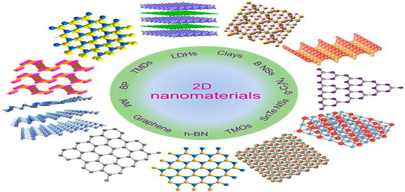
From basic 2D materials (such as stannene, borene, and black phosphorus) to layered double hydroxides (LDHs), graphite carbon nitrides (g-C3N4), and many more, we have discovered a vast array of 2D nanomaterials (NMs), graphene, hexanol boron nitride (h-BN), transition metal di-chalcogenides (TMDs, such as MoS2, WSe2, and PtSe2), graphene, and many more. 9 – 17 These materials are like graphene because they have a layered structure. Electron mobility is restricted to nanometer lengths, equivalent to several thick atomic layers thickness. In contrast to one-dimensional (1D) and three-dimensional (3D) NMs, two-dimensional (2D) NMs offer the following benefits:
A perfectly manageable stiffness, typically between a few and tens of nanometers, that is possible to achieve using a variety of preparation methods. 18
A unique electrical structure consists of a band structure, a discrete Fermi surface, and a controlled band gap. 19
They are more reactive and have a better capacity to absorb because of their large specific surface area. 20
Distinctive optical and electrical characteristics include remarkable fluorescence, Raman scattering, and light absorption. 21
Modifiable chemical and physical characteristics, including electrochemical activity, electrical conductivity, band gap, etc.
Due to their many benefits, 2D NMs have great promise in different sectors, including electronics, opto-electronics, sensing, adsorption, catalysis, and sensing. 21 – 23 Because they have a lot of surface area, strong co-valent bonds within layers, and weak van der Waals interactions between layers, TMDs are great for counter electrodes (CEs) in dye-sensitized solar cell (DSSC) devices. They are also very good at conducting electricity. TMD-based electrocatalysts are essential for redox reaction facilitation in DSSCs. It has been shown that TMDs’ electrochemical activity may increase significantly by keeping a steady supply of electrons on their surface. 24 , 25 Preparing and synthesizing 2D NMs is a significant obstacle to their present development. To make two-dimensional NMs, you can use chemical and physical methods such as mechanical exfoliation, ion intercalation, ultrasonic-assisted liquid phase exfoliation, chemical vapor deposition (CVD), and hydro-thermal synthesis. 26 – 29 Furthermore, the preparation conditions of the 2D NMs influence their characteristics. 30 , 31 Investigating the economical and effective 2D nanomaterials synthesis and improving their functioning in the pertinent application sectors is extremely important.
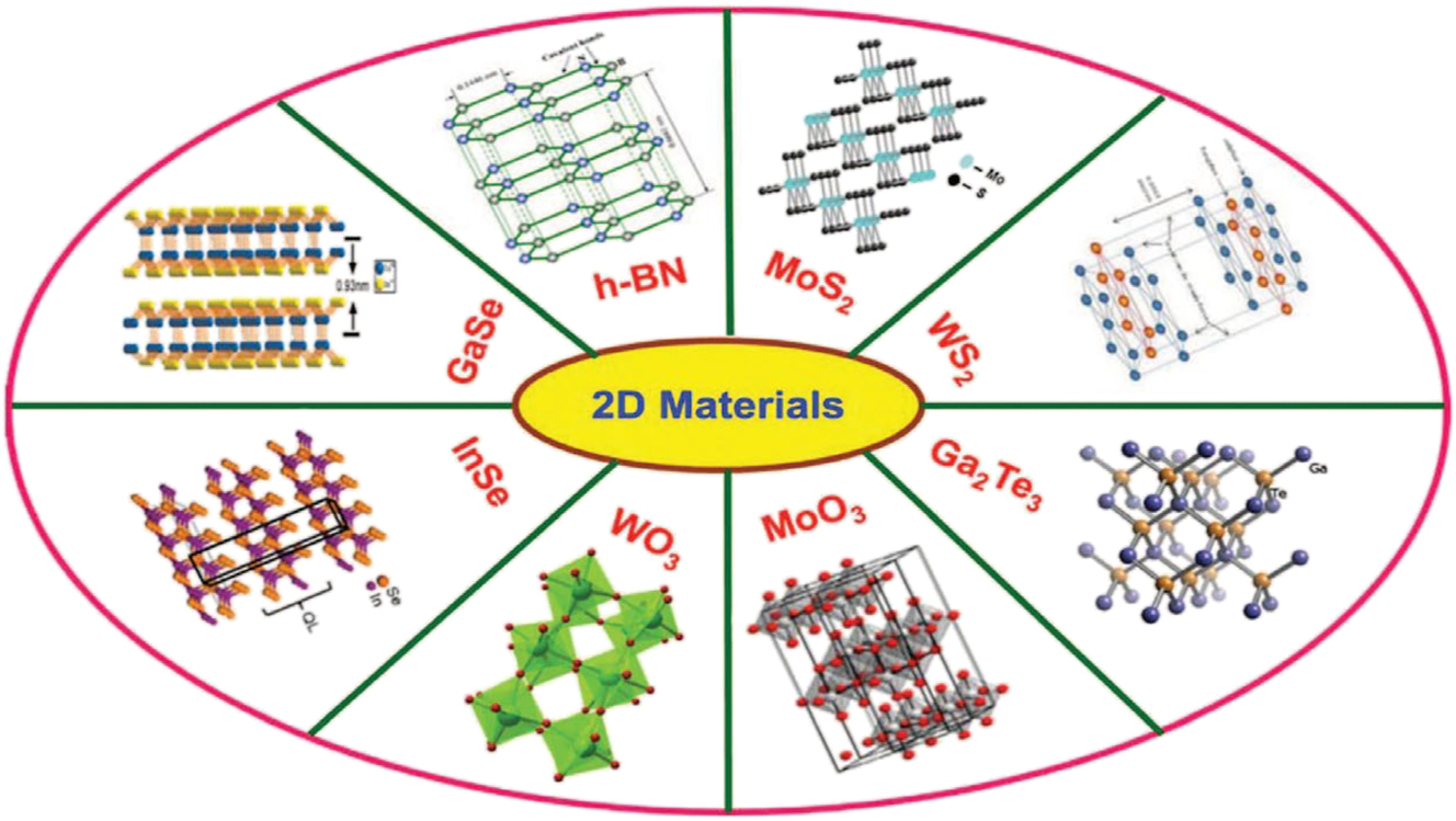
2D layered inorganic nanomaterials (2D-LINs) are a new type of inorganic layered material with intriguing physical and chemical properties; nonetheless, most of the research has been on graphene and its applications. 32 , 33 Hexagonal boron nitride (h-BN), molybdenum disulfide (MoS2), tungsten disulfide (WS2), indium selenide (In2Se3), gallium selenide (GaSe), vanadium selenide (VSe2), iron sulfide (FeS), tungsten selenide (WSe2), molybdenum selenide (MoSe2), gallium telluride (GaTe), and gallium sulfide (GaS) are examples of such 2D inorganic nano-materials. 15 , 34 Recent reports have highlighted the use of 2D-LINs in innovative electronic devices, including gas sensors, field emitters, electrochemical sensors, biosensors, solar cells, and gas sensors. This study reviews 2D NM preparation techniques and addresses the benefits and drawbacks of each technique. Additionally, this website includes an explanation of how 2D NMs are utilized in many sectors, including photodetectors, sensors, lithium-ion batteries, electromagnetic wave absorption, and photocatalysis. The present challenges of further developing 2D NMs are also addressed. Enhancing their utilization in electrochemistry, photocatalysis, sensor technology, and electrocatalysis, this review will facilitate the development and preparation of high-quality, high yield 2D NMs.
2 Primary morphological parameters of 2D-NMs
Electrical, optical, and mechanical characteristics are the main physical attributes of two-dimensional nanometers. Physical characteristics like thickness, size, and surface flaws can be changed to affect these properties. 26 , 35 There is hope that these methods can reduce production costs while simultaneously increasing output of high-quality nanomaterials. Nanomaterials’ electrical characteristics are influenced by their composition as well. The remarkable potential of novel nanomaterials such as metal-organic frameworks (MOFs), carbon–organic frameworks (COFs), and metal Xenes for use in electrochemical devices has attracted a lot of interest. 29 , 30 , 36 Structure of different types of nanomaterials are shown in Figures 1 and 2.
Different type of structure of organic nanomaterials. Copyright from John Wiley & Sons. Carbon-based Nanomaterials. 13
Structures of 2D nanomaterials. Reproduced with permission (Hu et al. 2019, Copyright from Elsevier).
2.1 Size and shape of 2D-NMs
Reducing the size and shape of 2D NMs can efficiently fine-tune their physical properties. When the size of 2D NMs gets close to the normal length scale of electrons, their electrical properties show quantum confinement effects. This causes discrete energy levels and band-gap modulation. Semiconducting behavior results from an increase in the bandgap with decreasing size. It is possible to customize the conductivity and band structure of 2D NMs for purposes due to the size-dependent tunability of their electrical properties. 37 , 38 You may alter the optical properties of 2D NMs, such as absorption, emission, and light–matter interactions, by changing their diameters. Because the absorption and emission spectra are so sensitive to changes in the material’s size-dependent energy band structure, the range of wavelengths at which the material may absorb or emit light can be precisely controlled.
In addition, small-scale quantum confinement effects can generate size-dependent photo-luminescence, where the emission wave-lengths shift towards higher energies with decreasing size. 39 , 40 Size changes in 2D NMs can control their chemical reactivity. Reactive site density rises with decreasing size because of an increased edge-to-bulk atom ratio. The material’s reactivity towards chemical species may be enhanced by its greater surface-to-volume ratio, making it suitable for catalytic applications. 39 , 41 , 42 A variety of 2D inorganic mateials that are being used are shown in Figure 3.
Example of 2D inorganic materials. Copyright from Nanoscale (2015).
2.2 Thickness of 2D NMs
Their thickness strongly influences the electrical, optical, and mechanical properties of 2D-nanometer nanostructures. Its thickness determines a 2D material’s electronic band structure and electron transport qualities in terms of electrical properties. The band structure of 2D NMs varies with decreasing thickness, which modifies the electron’s band gap. Larger band gaps are typically found in thin 2D NMs, which lead to improved carrier mobility and higher electron transport properties. The 2D nanostructures’ optical absorption, transmission, and reflection properties are affected by their thickness. More efficient optical absorption rates are a result of the thin 2D NMs’ ability to absorb incoming light. As a result, the efficiency of photoelectric conversion is enhanced, and the reaction time to light is accelerated. Their mechanical characteristics are likewise impacted by the 2D NMs’ thickness. Thin 2D NMs are more adaptable to different surface topographies and strain situations because to their enhanced flexibility and bendability. In conclusion, 2D NMs’ mechanical, optical, and electrical characteristics may all be accurately adjusted by varying their thickness, which improves their performance. 43 , 44
2.3 Surface defects of 2D NMs
The surface imperfections of 2D NMs have a major effect on their physical properties. Imperfections on the surface can alter the band structure, cause electron scattering, and alter the conductivity and carrier transport by introducing new energy levels. The material’s electron transport properties can also be compromised by surface flaws, which can lead to charge localization and shorter electron lifetimes. The optical transmittance, refractive index, and absorption of a material can be altered by surface defects. Optical properties including luminescence and optical transparency might be affected by these alterations. 45 Finally, 2D NMs’ mechanical, optical, and electrical properties are greatly affected by surface flaws. Therefore, while designing and implementing 2D NMs, surface defects must be taken into account and handled.
3 Preparation of 2D-NMs
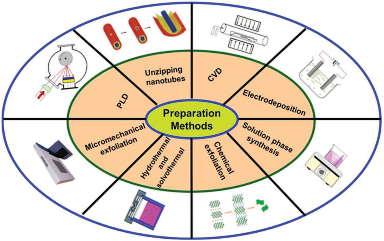
Depending on the desired application sector, there are different conditions for external structure, lateral dimensions, and microstructure when creating 2D nanostructures, which are of major relevance for related research. With the advancement of research, the methods for preparing 2D NMs have become more varied and can currently be roughly categorized into “top-down” and “bottom-up” techniques. 14 , 17 , 46 The properties of various materials, or even the same material made by different preparation methods, will exhibit some degree of variation.
A simple method that yields a lot of inorganic 2D nanomaterials is liquid exfoliation. Their employment in the fabrication of devices is limited by the non-uniform shape and dispersion of the as-prepared product thus far. Another practical technique for mass producing atomically thin layers of 2D metal chalcogenides is chemical vapour deposition. Metal chalcogenide thin films have also been produced electrochemically. Nevertheless, rather than discussing nanosheets or nanoribbons, the majority of the documented literature on electro-deposition focuses primarily on the synthesis of various metal chalcogenide nanostructures. Therefore, creating novel techniques for the easy and controllable scalable manufacturing of layered inorganic nanomaterials remains a significant issue in the context of both physical and chemical processes. 47 – 49
A significant obstacle in creating sensors with real-world uses is creating sensors based on 2D materials that have longer lifespans and better durability. To achieve good sensitivity with a very low detection limit in electrochemical sensors, nanocomposites of metal chalcogenides with diverse new materials need to be investigated. The development of sensor devices is heavily dependent on the surface area of active materials. It is frequently necessary to functionalize the surface in order to alter its sensory characteristics. By doping semiconducting materials with noble metals like Au, Ag, Pd, and Pt, one can adjust and modify their band gap. 38 , 50 Therefore, more research is required to determine how the dopant affects the electrical structure of 2D organic materials, there are different synthetic approaches for 2D inorganic layered nanomaterials as depicted in Figure 4.
The range of different synthetic approaches that are being used to fabricate/synthesize 2D layered inorganic nanomaterials (NMs). Copyright from John Wiley & Sons, Inc. Carbon-Based Nanomaterials (2016).
3.1 Top-down method
Removing matrix material by applying external force in a progressive manner is what top-down preparation is all about. The top-down approach is based on the exfoliation of 2D crystals from their bulk crystal parent. It should be highlighted that only materials having layered compound bulk crystals may be treated using top-down approaches. 51 We have concentrated on ion intercalation-assisted exfoliation, ultrasonic-assisted liquid phase exfoliation, and mechanical peeling in this review.
This method primarily use solid and state processing techniques to break down large materials into smaller particles using physical operations such as crushing, milling, and grinding. In general, this approach is unsuitable for producing uniformly shaped nanomaterials, and achieving extremely small nanoparticles is quite challenging, even with substantial energy consumption. The primary challenge associated with this approach lies in the limited availability of surface structure, which exerts a substantial influence on the physical properties and surface chemistry of nanomaterials.
3.1.1 Mechanical peeling
Geim and his colleague Novoselov used mechanical exfoliation, or repeated peeling, for the first time in 2004, to produce high-quality graphene sheets that were only a few atomic layers thick (Figure 1a). By using ball milling, certain adhesive tapes, and other techniques, the mechanical peeling process applies an external force to the matrix material. To generate 2D NMs, the matrix material is pulverized as a consequence. 52 This economical approach guarantees good sample purity because it doesn’t require chemical reagents or reactions during preparation. However, it has several disadvantages, such as limited yield, poor controllability, and the inability to prepare on a large scale and in a broad region.
Huang and colleagues 53 proposed a revolutionary approach to graphene preparation. Throughout the preparation method, aluminum (Al) is employed as a grinding aid; the particle diameter ratio of Al is 200.0 mesh–500.0 mesh, or 1:1.884. A specific surface area of 542.6 m2 g−1 was achieved by the manufactured graphene, making it extraordinary. It typically had less than five layers and a yield of more than 90 %. The graphene sample, however, is vulnerable to degradation by the Al-removing detergent. Sun et al. 54 overcame this issue by employing polycrystalline thin films of metals such as Ag, Au, Fe, Cr, and others as substrates. 2D NMs such graphene, FeSe, phosphorene, and MoS2 were effectively created after placing the substrate and crystal in an ultra-high vacuum (UHV) for a few minutes (Figure 5b and c). This technique has several applications. When making 2D NMs, treating the precursors is a crucial step. The predecessor in the study by An et al. 55 was pabex, which was heated to 200 °C and then exfoliated with BN solid powder. As you can see in Figure 5d, high-resolution transmission electron microscopy (HR-TEM) pictures of the finished products were used to learn more about their microstructure.
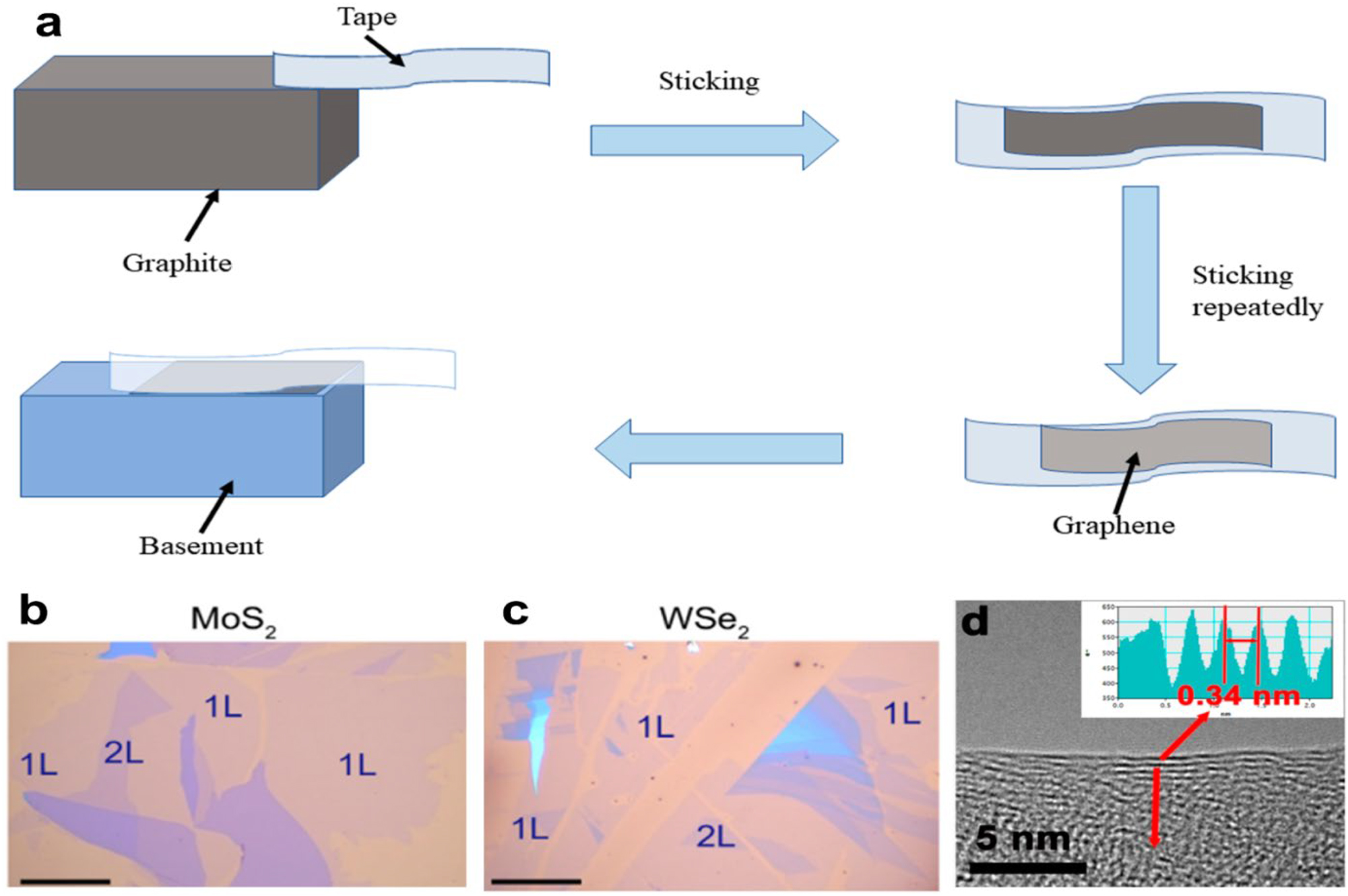
Preparation of 2D NMs. (a) Mechanical peeling mechanism. (b) UHV mechanical exfoliation optical pictures of large-scale 2D materials onto polycrystalline Au: MoS2 and WSe2. (c) Each photo shows 1 L and 2 L. Scale bar: 40 µm. 54 2022 Science Bulletin copyright. (d) Five-layer Pebax-BNNS HRTEM picture. The distance profile of the red line in d indicates a 0.34 nm crystal separation (inset). 55 Copyright 2019, NPJ 2D Materials and Applications.
Because of their malleable physicochemical properties – their melting point, wettability, electrical and thermal conductivity, catalytic activity, light absorption, and scattering nanoparticles and nanomaterials have become more important in technological developments. You can change the attributes (electrical conductivity, color, chemical reactivity, elasticity, etc.) of nanostructures by manipulating their size, shape, and internal order. One of the biggest obstacles is the large-scale production of nanomaterials for real-world use. On the other hand, numerous synthesis methods have been developed, including solution-based methods, template-based approaches, and microwave-assisted synthesis.
Due to straightforward techniques and no need for solvents, functionalized BN Nano-sheets (NSs) were formed throughout the preparation process. The sample shows good water dispensability and does a good job of preserving the lamellar structure during rubbing. Deng et al. 56 used micromechanical exfoliation to create a small number of layered MoS2 flakes that had creases. Compared to the flat region, the wrinkled part had a much higher carrier mobility measured at 30 K (µw = 5.55 cm2 V−1 s−1) than the flat region (µf = 1.42 cm2 V−1 s−1). Tensile strain-induced wrinkles in MoS2 are responsible for the reduction in lattice scattering and the suppression of electron-phonon interaction, which leads to an increase in carrier mobility. Carrier mobility is important in deciding the frequency at which electronic devices operate. For instance, in bipolar transistors, a crucial constraint on frequency response characteristics is the time it takes for a few carriers to transit the base region. Device performance may be improved, and this transition time can be significantly decreased with increased carrier mobility. Strain can potentially dramatically boost 2D NMs’ carrier movement under some circumstances.
3.1.2 Ultrasonic-supported liquid phase exfoliation
Ultra-assisted liquid-phase exfoliation (UALPE) uses ultrasonic waves in a solvent to separate bulk materials from top to bottom. Figure 6a shows the method that overcomes van der Waals forces between material layers. 61 , 62 Since it must match the stripped material’s surface tension, the solvent’s choice affects 2D NM surface shape and stability.
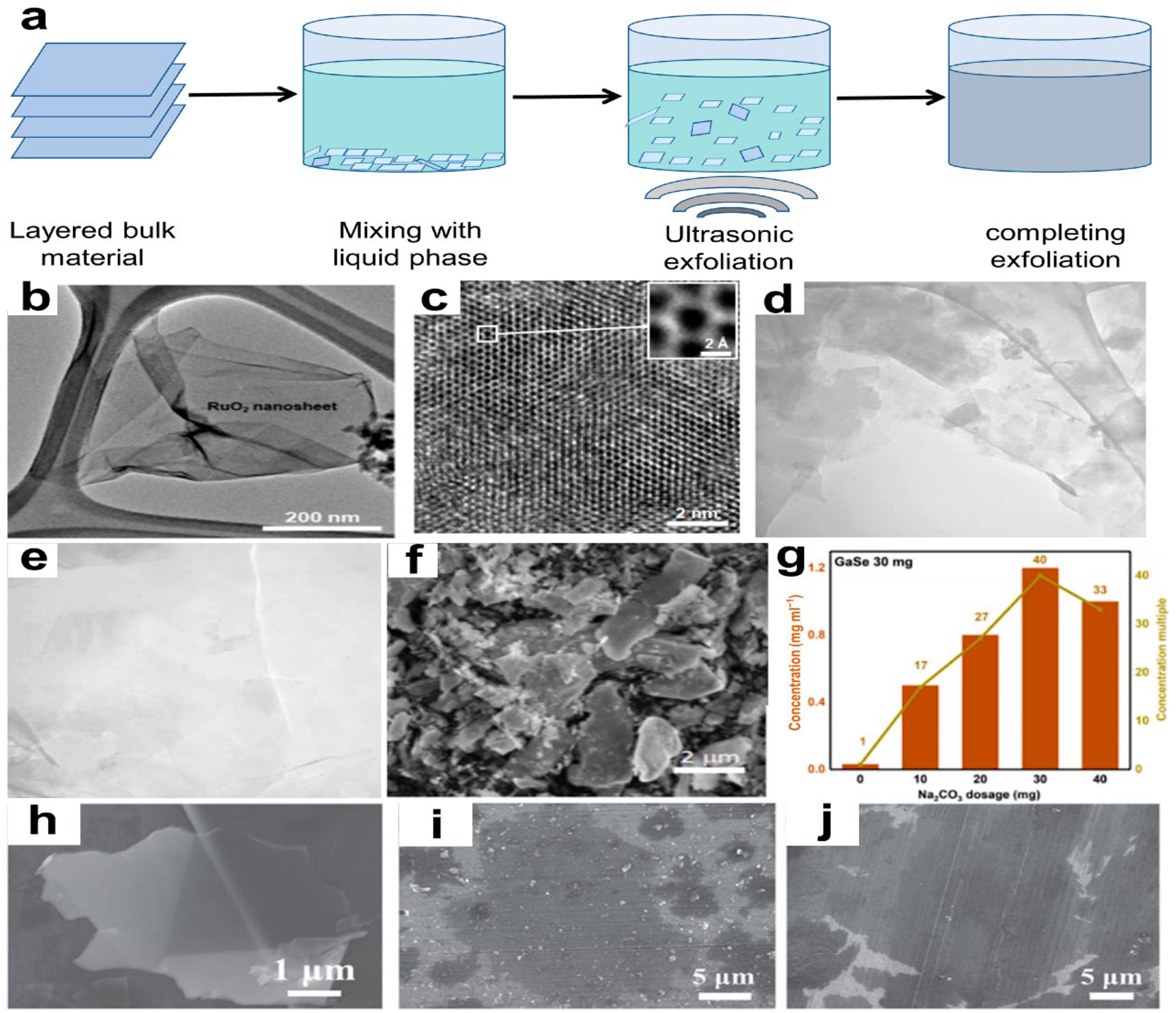
Ultra-assisted liquid-phase exfoliation (UALPE) of 2D NM surface. (a) UALPE mechanism diagram. (b) TEM and (c) Monochromatic Cs-corrected HRTEM images of exfoliated RuO2 nanosheet after 60 min of ultrasonication. 57 Inorganic Chemistry Frontiers copyright 2021. (d) and (e) TEM micrographs of exfoliated graphene fakes, size bars: 200 and 100 nm. 58 Scientific Reports copyright 2022. (f) Sample SEM (30 mg Na2CO3). (g) Sample and multiple-to-blank control group concentrations. 59 Materials Letters copyright 2021. SEM pictures of (h) graphene, (i) MoS2, and (j) WS2 nanosheets. 60 Small copyright 2021.
The liquid phase’s main role in stripping is efficiently transmitting energy and peeling materials under shear strain. The liquid phase also lubricates and cleans, allowing high-quality 2D NM manufacturing. Various liquid phases have various peeling efficiencies. Therefore, target materials must be carefully selected. The liquid phase for GaSe preparation should be isopropanol acid (IPA). 63 An aqueous surfactant solution was mixed with graphite and subjected to ultrasonic exfoliation. 64 Graphene-like materials have a lamellar structure, outstanding electro-chemical performance, and great flexibility. Kim et al. 57 found that ultra-sonic treatment of a RuO2 ion mixture after three days of ion exchange increased RuO2 NS production by 50 %. A lengthy ultrasonic duration lowered RuO2 NS lateral dimension and peeling energy (Figure 2b and c). Additionally, Mushfq et al. 58 , 65 examined how ultrasonic duration and power affect the quality and production of one-to three-layered graphene samples. Ultra-sonication for 55 min at 264 W yields the best sample quality and yield. TEM pictures show exfoliated multi-layer (<10 layers) and less layered (one–three layers) samples with superior quality and smaller graphene flakes (Figure 2d and e). Qi et al. 59 suggested a practical and effective technique for making GaSe NSs by adding Na2CO3 powder to IPA, which increased exfoliation yield by 40 times (Figure 2f and g). Simple, cheap, and easy to use, this approach may peel other 2D NMs. By adding small amounts of Al2O3 abrasives to the precursor solution during ultrasound liquid-phase processing, Shi et al. 60 came up with a new ultrasonic-ball milling method that makes a lot of high-quality ultrathin 2D NMs with large transverse sizes. This approach yields flake graphite, MoS2, and WS2 NSs with lateral sizes of 1–20 µm and thicknesses of 1–3 nm, yielding over 20 % (Figure 6h–j). The strategy’s universality is seen here.
3.1.3 Ion intercalation-assisted exfoliation
Ion intercalation-assisted stripping is a new method for the controlled synthesis of large-sized, high-quality 2D NMs. Intercalation compounds are made by inserting smaller cations, such as lithium, into spaces between crystals. These compounds can create new spaces by filling them with lithium ions (Li+) and changing their phase. 66 This process produces layered materials. Figure 7a displays the method’s mechanism diagram. It is still challenging to properly regulate the quantity of ion intercalation even though this approach produces large numbers of 2D-nanaomaterials.
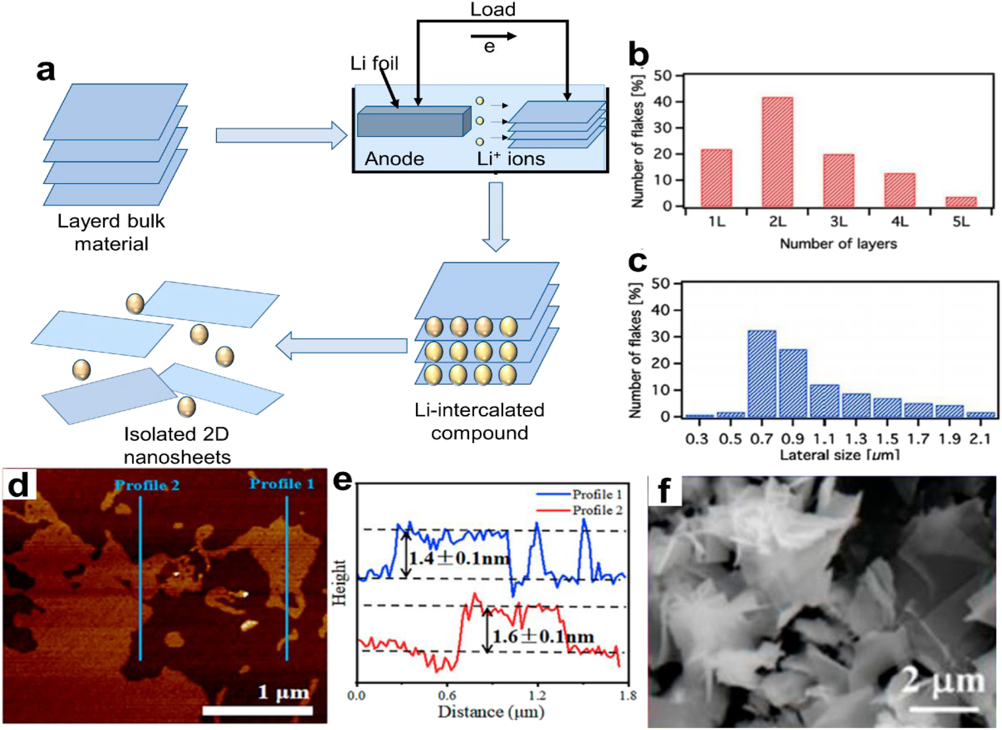
Ion intercalation-assisted exfoliation for 2D NMs. (a) Ion intercalation-assisted exfoliation method’s mechanism diagram. (b) The chunkiness division derived from observations of 60 distinct nanoflakes using scanning transmission electron microscopy (STEM). (c) Distribution of lateral sizes using information from 150 distinct nanoflakes. 67 © 2018 Flat Chem Copyright. (d) Ti3C2Tx AFM picture and (e) matching peak shapes El Garah et al. 68 Science, Copyright 2022. (f) WS2 nanosheets exfoliated in a SEM picture. Results of the appropriate places’ energy dispersive X-ray (EDX) element analysis are shown in the inset (f) (Tian et al. 69 Crystal Research and Technologies, Copyright 2021.
An experiment by El Garah et al. 67 used lithium-ion interaction to peel off MoS2 in less than an hour. Lithium chloride (LiCl) in dimethyl sulfoxide (DMSO) was the solvent of choice. The MoS2 bulk crystal is subjected to stretching and intercalation for a duration of 45 min with a 1 M LiCl solution in DMSO serving as the electrolytic species and Li+ resource. The sample has potential applications in low-cost opto-electronic devices. We analyzed 150 nanoflakes from one batch using scanning transmission electron microscopy (STEM), and 60 nanoflakes from the other batch using HRTEM (FEI Tecnai F20 TEM paired with a Schottky emitter), to do statistical tests on them to find out how big and thick they were. The study found that thick MoS2 nanoflakes with a side length of about 0.8 µm were present in large amounts in single, double, and triple layers. Adding several processes together is another way to increase the yield. To make ternary-cation-intercalated Ti3C2Tx MXene NSs, Xv et al. 68 used mixed fluoride salt wet etching and an alkalization process. Li, K, and Na ions were progressively added to multilayered Ti3C2Tx to increase the spacing between the layers and reduce the contact forces in a targeted manner. This resulted in a high surface area (92.6 m2 g−1) and precise angstrom-level structural control. The atomic force microscope (AFM) picture is displayed in Figure 3d and e. Using a single Li+ intercalation, the yield of scattered Ti3C2Tx may increase from 45 % to 62.9 % compared with a standard approach.
Additionally, Tian et al. 69 used Li+ intercalation exfoliation to produce WS2 NSs. According to their study, as shown in Figure 7f, this procedure makes constructing WS2 NSs on a large scale possible. It produces a bigger lateral size and a clearly described lattice formation without elemental contaminants. Furthermore, the addition and de-insertion of Li+ have significant uses in the 2D MoS2 phase shift. For example, Hou et al. 70 were able to make trigonal MoS2 (1T-MoS2) by taking Li atoms out of hexagonal MoS2 (2H–MoS2) and then adding 20 % ion atoms.
3.2 Bottom-up-method
The production of ultrathin 2D NMs is accomplished by bottom-up methods, such as the meticulously orchestrated chemical reactions of identified components performed under well specified experimental conditions. This bottom-up method offers the possibility of unlimited flexibility, which might lead to the creation of several types of ultrathin 2D NMs. Some methods that may be used to make big 2D NMs with good microstructure include hydrothermal method, atomic layer deposition (ALD), chemical vapor deposition (CVD), and physical vapor deposition (PVD). The focus of this review is on these methods. Using this approach, a significant amount of materials are made by preparing them atom by atom or molecule by molecule. The majority of nanomaterials are produced more regularly using this technique. This process can yield nanomaterials with a consistent size, shape, and distribution. In order to stop unwanted particle growth, it essentially accurately controls the chemical synthesis process. 71 , 72 When producing and processing nanomaterials with improved shape and particle size dispersion, this technique is crucial. The fact that the methods used to produce the nanoparticles are affordable and environmentally friendly is another significant aspect (Figure 8).
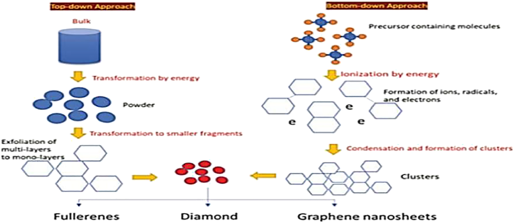
Diagrammatic representation of top-down approach and bottom-down approach of making of nanomaterials. Copyright from, J Solgel Sci Technol, (1998).
3.2.1 Vapor deposition
3.2.1.1 Chemical vapor deposition (CVD)
The key CVD process for 2D NMs involves reacting two or more solid-source materials in a reaction chamber to make them gaseous. Chemical reactions generate hazardous species that are afterwards transported to accumulation site and applied to the substrate. It is common practice to employ this method when fabricating 2D NMs with very thin layers. Figure 4a shows a schematic of the CVD process’s mechanisms. Using inert gases such as N2 and Ar as auxiliary agents could reduce film wrinkling and increase flatness. 73 This strategy offers more control and eliminates the possibility of contamination during preparation as compared to the “top-down” method. Additionally, its versatility adds to its value. Some of its downsides include expensive prices, unpredictable raw material prices, and inefficient use of reactants.
Using a space-limited CVD technique, Chen et al. 74 synthesized BiOBr NSs from BiBr3 powder and oxygen. Two mica substrates were stacked on top of one another on a quartz yacht positioned in the center of the thermal region. Figure 4b and c shows that the space-confined CVD-grown BiOBr nanoflakes have transparent excellence and remarkable UV photo-detecting capabilities. The researchers Gao et al. 75 grew multilayer MoS2 over molten glass, which resulted in bigger samples with smoother edges.
Figure 4d shows that the sample exhibited outstanding electrical properties and a maximum single crystal size of 563 µm. As before, sapphire was warm up to 1400 °C and injected with CH4 to serve as the graphene growth substrate in the study by Chen et al. 76 With single-layer characteristics and a high carrier mobility of 14,700 cm2 V1 s1, the resulting graphene sheet is very desirable. There are no indications of contamination or poor homogeneity in the graphene/sapphire interaction, as demonstrated in Figure 4e, a cross-sectional transmission electron micrograph. A two-dimensional model of diffusion-limited aggregation (2D-DLA) was developed by Li et al. 77 using a growth mechanism at the atomic scale. They achieved this by fabricating graphene with less defects and greater uniformity through the application of a modified classical fractal theory. Multiple 2D NMs were synthesized by CVD using a technique based on fractal growth. A graphene sample with surface pores was first created via CVD. According to Figure 4g, the growth conditions were as follows: CH4 = 10 sccm, H2 = 10 sccm, and T = 1030 °C. Following this, they examined the 2D-DLA model and discovered that the gaps vanished, additionally, When the release rate of the active carbon atoms was drastically lowered, the simulated patterns started to look like regular hexagons (Figure 4h). The rate of active carbon atom generation was reduced when, using these data as a basis, they raised the H2/CH4 ratio to 50 cm by 5 cm at the identical temperature for growth i.e. 1030 °C. They were able to utilize CVD growth to create a hexagonal graphene domain of excellent quality, devoid of defects (Figure 9i).
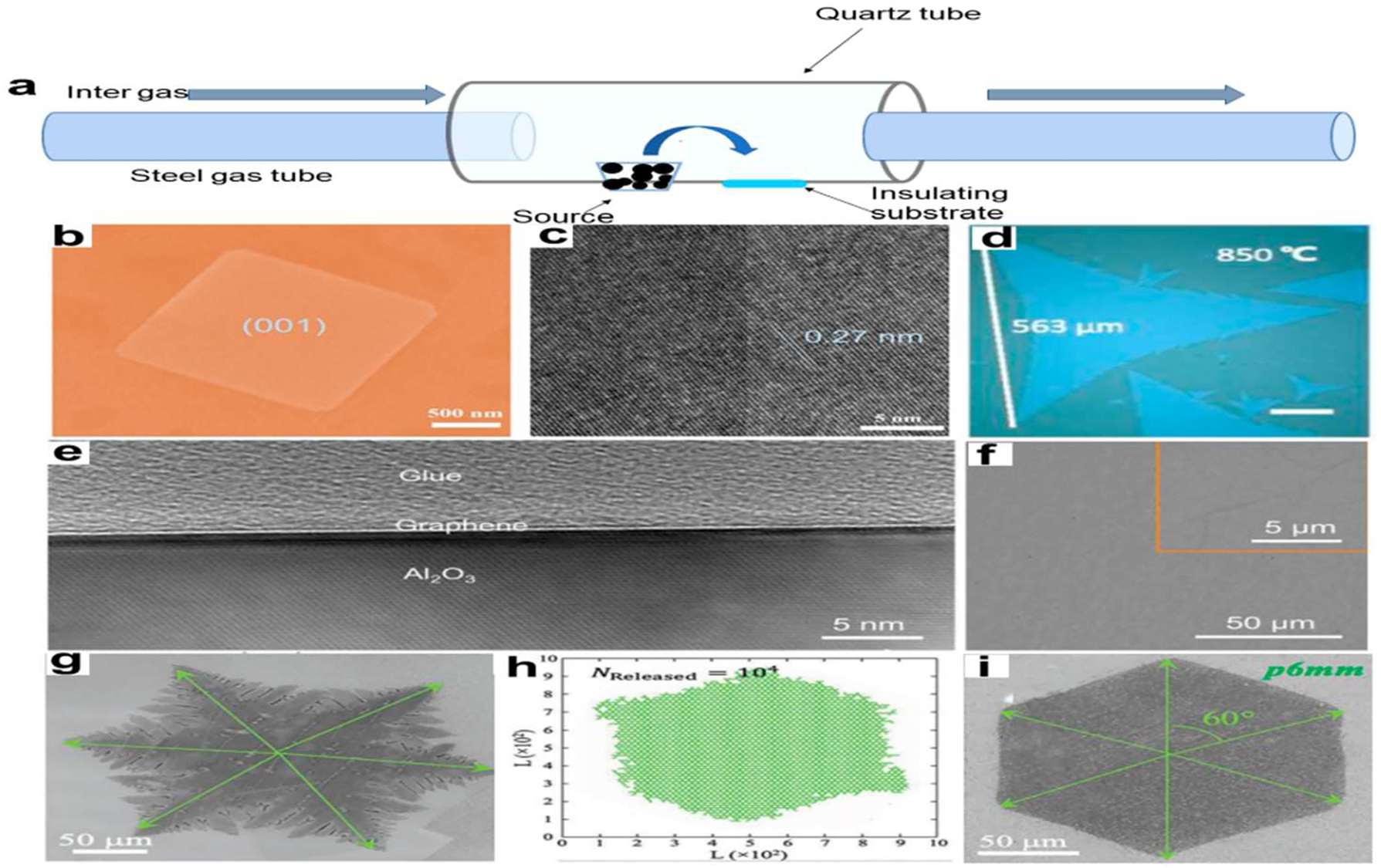
CVD process for 2D NMs. (a) A representation of the CVD mechanism. (b) A 2D BiOBr flakes SEM picture. (c) 2D BiOBr flakes HRTEM picture. 74 Journal of Materials Science & Technology, copyright 2020. (d) Substantial solitary-crystal monolayer MoS2 optical picture. Bar scale: 100 µm. 75 2018 Applied Physics Letters All rights reserved. (e) Comprehensive cross-sectional transmission electron microscopy picture of sapphire-grown graphene. (f) Typical sapphire-based graphene as-grown SEM picture. The high-magnification SEM picture of graphene is seen in the inset. 76 Science Advances, Copyright 2021. (g) CVD-synthesized common-shaped graphene (scale bar: 50 µm). (h) A 2D-DLA simulation pattern using the quasi-3D-release mode, allowing the simulation output to show any defects. (i) A perfect hexagonal graphene domain with a scale bar of 50 µm was created using a greater H2/CH4 ratio. 77 Advance Materials Copyright 2019.
Essentially, this technique involves treating the substrate with volatile precursors that interact with its surface to create the desired films. Typically, the reaction chamber’s gas flow eliminates volatile by-products. Temperature, reaction rate, and precursor quantity are just a few of the variables that have a big impact on the quality of the materials that are deposited on the surface. It has been reported that the CVD approach was used to manufacture Sn4+ doped TiO2 nanoparticle films. 64 , 74 By using the CVD technique, another doped TiO2 nanoparticle was created. In this process, the kind and quantity of cations present in the chemical reactions cause TiO2 to crystallize into rutile structures.
One technique that permits epitaxial growth in the vapour phase is metalorganic chemical vapour deposition (MOCVD), which was developed from the vapour phase epitaxy (VPE) approach. Organic molecules from periods III and II, along with hydrides from periods V and VI, are the starting points for the MOCVD process. Several III-V II-VI compound semiconductors and their multilayer solid solutions can be created by MOCVD using thermal breakdown processes in VPE on a substrate, resulting in thin-layer single-crystal materials. 78 At 240 °C, Song 79 utilized a metal-organic CVD technique using a liquid germanium precursor to create rectangular-shaped 2D-layered Ge4Se9. They were able to accurately manage the precursors’ breakdown in the first heating zone (T 1 = 480 °C) and the crystal formation in the second heating zone (T 2 = 240–400 °C) thanks to their MOCVD reactor’s two-zone heating technology. Muscovite mica served as the experimental substrate, whereas dimethyl selenide (CH3)2Se and Ge(dmamp)2 were the precursors for Se and Ge, respectively. Li et al. 80 detailed core–shell NMs using Au–MoS2, a heterogeneous core–shell material that has great promise for applications in sensors, optoelectronics, and optical imaging in the future. The growth of fullerene-like MoS2 shells on Au nanoparticles was achieved by a modified CVD technique.
3.2.1.2 Physical vapor deposition (PVD)
Physical vapor deposition (PVD) is commonly used to create 2D-nanometer layers. This method creates a thin layer by vaporizing a solid material, which is desubstrate. PVD has several benefits, including precise control, homogeneous film deposition, and high purity. However, it has several drawbacks, including restricted material choices, the need for an extreme vacuum condition, and comparatively sluggish progress levels. 81 Through magnetron sputtering, the impact of gamma-ray irradiation on MoS2 thin films was studied by Anbalagan et al. 82 Their experimental results demonstrated that thinned-out sputtered MoS2 films exhibit long-range ferromagnetic (FM) behavior at room temperature, with a magnetization (Ms) of about 610 emu/cm3 (Figure 5a), following nine kG of gamma-ray irradiation. MBE, or molecular beam epitaxy, is a significant PVD technique. It is possible to use stanene and borophene with this effective approach. The first ultrathin borophene sheets were synthesized under UHV conditions by Mannix et al. 83 using a 99.9999 % pure solid boron atomic source. Figure 10b displays a picture of a scanning tunneling microscope (STM). This method was selected to overcome the difficulties associated with hazardous precursors.
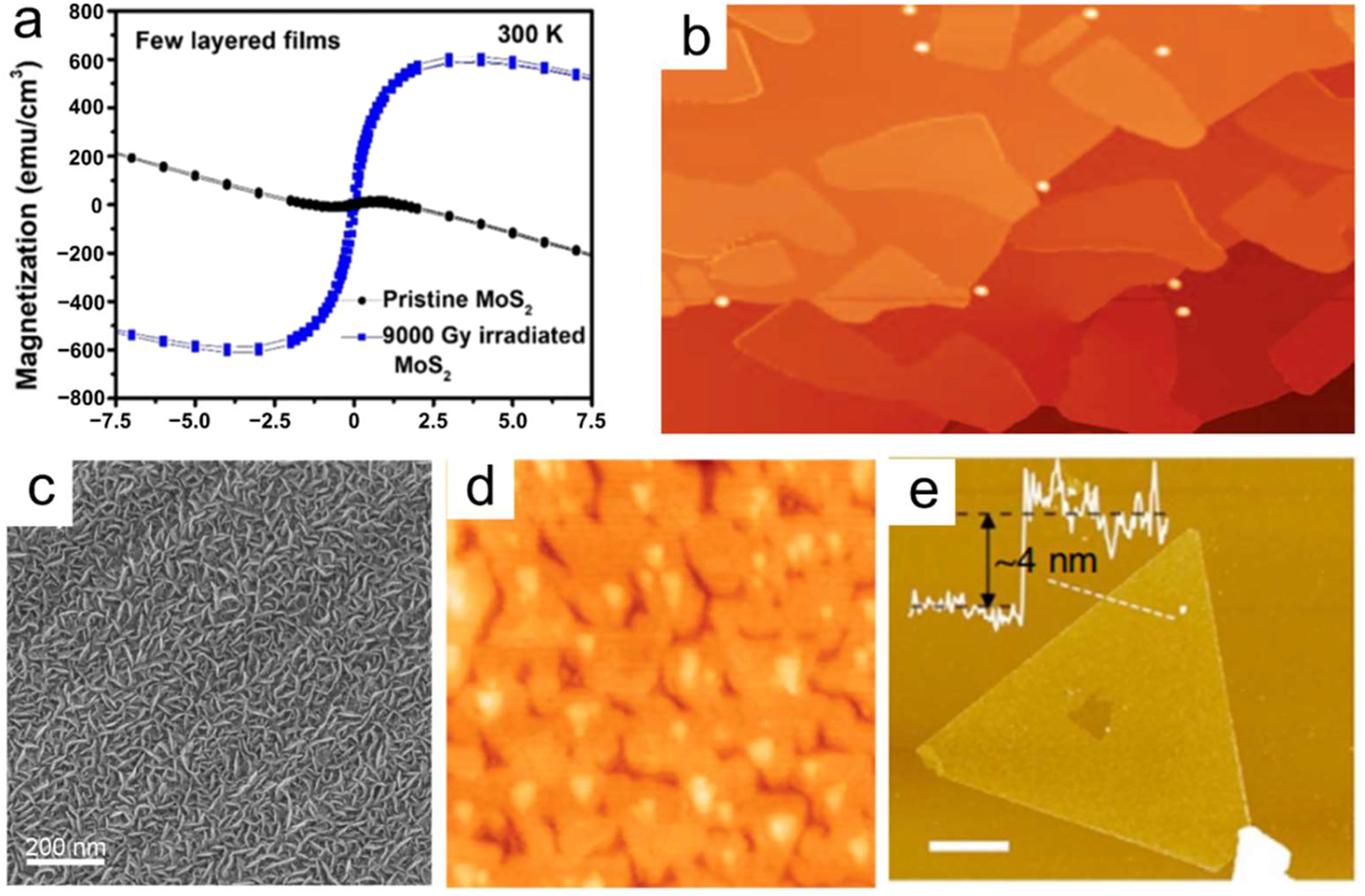
PVD of 2D NMs. (a) Magnetization for MoS2 films before and after 9.0 kGy irradiation observed at 300 K versus applied magnetic field. 82 All Rights Reserved, ACS Nano. (b) A large-scale STM topography picture of sheets of borophene. There is a 100 nm 83 scale bar. Science 2015 All rights reserved. (c) Under 100 W of sputtering power, SEM pictures of MoS2 nanostructured films were produced. 84 The Royal Society of Chemistry, all rights reserved. (d) Stanene (40 nm × 40 nm) zoomed-in STM picture. 85 Nature Materials 2015 All rights reserved. (e) An average triangular antimonene sheet as seen in an AFM scan. There are 4 nm thicknesses. One µm is the scale bar. 86 Nature Communications (2016) All rights reserved.
In their study, Zhang et al. 84 used a magnetron sputtering method to directly PVD MoS2 nanostructures onto carbon fabric. They maintained a substrate temperature ranging from 450 °C to 700 °C with a boron flux of around 0.01 to 0.1 monolayer per minute (Figure 10c). The results demonstrated that nanosheet arrays with good definition could be created using 100 W of sputtering power and a gas pressure of 3 mTorr. Using MBE, Zhu and coworkers 85 synthesized ultrathin Sn films on a Bi2Te3 substrate with 2D stanene structures. Antimonene may find application in conductive electrodes that are both transparent and flexible. Figure 5d shows a scanning tunnelling micrograph (STM) of the stanene film enlarged. Ji et al. 86 created high-quality, fewer-layered antimonide polygons on a mica substrate using van der Waals epitaxy. Figure 10e shows that the antimonide polygons are as thin as 4 nm, which is equivalent to around 10 atomic layers. Additional experimental investigations into the unique characteristics and possible uses of antimonide can be initiated because of this study.
3.2.2 Hydro-thermal strategy
A specific precursor is cooked to high temperatures and pressures in an autoclave solution before the hydrothermal reaction can begin. Figure 5a shows the schematic of the mechanism. Following this, it must undergo a number of powder processing procedures for post-treatment, such as washing, drying, and separation. 87 With its straightforward operation, low costs, and consistent procedure, the hydrothermal method enables the production of 2D NMs of high yield and quality. In addition, different sizes and shapes of 2D NMs may be synthesized by modifying the reaction restrictions. 88
Liu et al. 89 adopted an innovative way to make 2D morphogenesis carbon in a simple single-use hydrothermal process by starting with different types of carbohydrates and the biomolecule guanine. Guanine stimulates the creation of 2D nanostructures during the hydrothermal process. This approach produces porous carbon with finesheets, a large surface area, and adjustable N2 doping (Figure 11b and c). Consequently, the sample shows exceptional catalytic performance. Furthermore, temperature is an important factor in creating 2D MoS2 nanocomposites. 2D MoS2 nanocomposites were synthesized by Long et al. 90 by means of an easy hydrothermal process. This produced very thin NSs with an average width of 130–330 nm and a thickness of 6–13 nm, or six to eight layers. Crystal quality improved and MoS2 grew along the c-axis when the hydrothermal temperature increased from 191 to 254 °C (Figure 11d and e). Researchers Marnadu et al. 91 investigated how changing the temperature of hydrothermal approach affected the structure and properties of 2D MoS2. Figure 6f shows the results of the experiments showing that the samples produced at 160 °C exhibit very interesting electrical properties. At a current density of 1 A g−1, this electrode had a maximum specific capacitance of 691 F g−1. It also showed high cyclic stability of 89 % over 5000 cycles. 2D inorganic nanomaterials have been synthesized using a wide variety of techniques, which details the many different processes that have been used in their synthesis. 90 The most basic and time-honored approach for creating high-quality, crystal-clear 2D nanomaterials from atomically thin layers is micromechanical exfoliation, sometimes known as the Scotch-tape method.
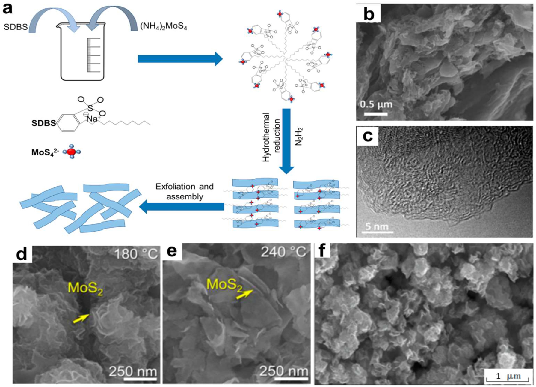
Hydro-thermal strategy of 2D NMs. (a) A hydrothermal method’s mechanism diagram, using the production of MoS2 with the help of sodium dodecyl benzene sulfonate (SDBS) as an example. The 2D porous carbon sample is shown in (b) SEM and (c) TEM pictures. 89 The Royal Society of Chemistry, all rights reserved. Synthesized 2D MoS2 field-emission SEM (FESEM) image at (d) 180 °C and (e) 240 °C. 90 Journal of Sol-gel Science and Technology, copyright 2023. (f) MoS2 nanoparticle SEM picture. 91 Inorganic Chemistry Communications, Copyright 2022.
3.2.3 Atomic layer deposition
To make atomic layer depositions (ALDs), gas-phase precursors are introduced into the reactor in pulses and then allowed to react and undergo chemical adsorption on the substrate. Isolating the individual reactants with inert gases (Ar, N2, etc.) enables layer-by-layer deposition and repeatable control of thickness. When it comes to making 2D NMs, the ALD process offers careful manipulation, regularity, and flexibility. The approach has a number of limitations, including expensive apparatus, slower growth rates, and restricted reaction circumstances. 92 The sulfurization of ALD-formed films of molybdenum oxide, which use ozone and Mo(CO)6 as precursors and produce a few layers of MoS2, was the focus of Martella’s 93 research. The quality of the final MoS2 layers was altered by controlling the development characteristics of the precursor film, which was achieved with ALD’s highly conformal growth capabilities. Over a cm2 sample area, four MoS2 layers grew consistently from precursors with a thickness of 4.0 nm. In Figure 12, the AFM picture is displayed.
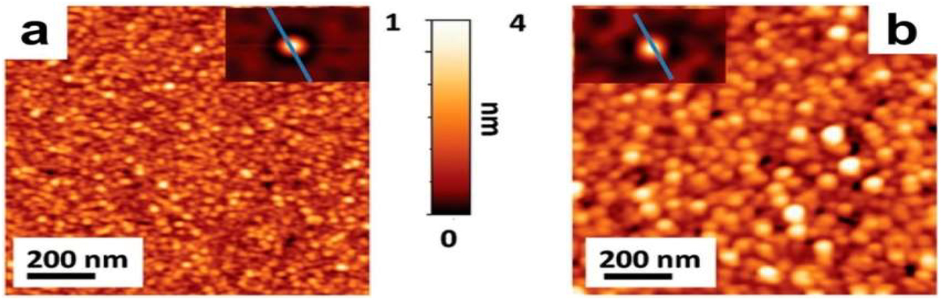
AFM topographic maps of (a) 4.0 nm thick ALD film precursor and (b) four MoS2 layers. The insets show the self-correlation functions calculated from the corresponding topographies. 93 Copyright from (2016), Advanced Electronic Materials.
In conclusion, there are a few drawbacks to using top-down approaches to prepare 2D NMs. The most notable ones are the inferior product quality, restricted application to certain materials, and limited controllability. They are inexpensive, work well in industrial settings, and need little in the way of preparation, among other benefits. Bottom-up approaches have the advantages of better controllability over the final products, improved quality, and the ability to synthesize almost any material compared to top-down methods. However, this strategy has significant disadvantages, such as large expenses and a comparatively poor yield 94 (Tables 1 and 2).
Some pros and cons of different approaches to 2D-MN preparation.
| Process | Methods | Advantages | Disadvantages |
|---|---|---|---|
| Top-down method | Mechanical peeling | High sample purity, cost effective | Low yield, poor controllability |
| Ultrasonic-assisted liquid phase exfoliation | Modifying the solvents affects the morphology and dimensions, easy technique | Small sample size, low yield, structural | |
| Ion intercalation-assisted exfoliation | High yield, high quality | Damage poor controllability, structural loss | |
| Bottom-up method | Bottom-up method | Keeping pollution at bay, exceptional controllability, high purity | High costs, low reactant utilization rates restrictions on the choice of materials |
| Physical vapor deposition | Uniform film deposition, precise control | Comparatively modest rates of growth in a high-vacuum setting | |
| Hydrothermal approach | Cheap, Precise Control | Prolonged reaction cycle, impure sample slower growth rate | |
| Atomic layer deposition | Regularity, flexibility | Equipment complexity, restricted reaction condition |
Morphological features and physiological properties of various nanomaterials which are synthesized via different methods.
|
Nanomaterials |
Synthesis method |
Morphological features |
Properties |
References |
|---|---|---|---|---|
| Metal oxides and hydroxides | Various synthesis methods | High surface area, redox properties | Suitable for electrochemical devices | [4] |
| Conducting polymers (e.g., polyaniline, polypyrrole) | Various synthesis methods | High conductivity, tunable redox potential | Versatile for electrochemical applications | [95] |
| Hybrid materials | Combination of nanomaterials class | Improved performance and functionality | Enhanced properties through synergy | [96] |
| 0D nanoparticles and nanodots | Various synthesis methods | Small size, high surface area | Promising for batteries, sensors, catalyst | [97] |
| 1D nanowires and 2D nanosheets | Various synthesis methods | Large surface area, excellent conductivity | Suitable for supercapacitors, fuel cells, and other electrochemical devices | [98] |
4 Applications of 2D NMs
Ultrathin 2D-structured nanomaterials have unique optical, chemical, electrical, and physical characteristics, making them potentially useful for various applications. These varied materials also have a wide range of compositions and characteristics, making them appropriate for several uses. Numerous domains, including electronics and optoelectronics, catalysis, energy storage and conversion, water purification, sensors, and biomedicine, have shown great promise for applying two-dimensional NMs. This section presents a thorough summary of the latest developments in the use of 2D NMs in several important applications, with a particular emphasis on their use in sensors, lithium-ion batteries, photodetectors, electromagnetic wave absorption, photocatalysis, and electrocatalysis. 99
Advantages of Nanotechnology
To enumerate the advantages and disadvantages of nanotechnology, let us first run through the good things this technology brings. It’s true that nanotechnology has the power to completely transform many electrical processes, goods, and uses. When it comes to electronic devices, fields such as nano transistors, nano diodes, OLED, plasma displays, quantum computers, and many more stand to gain from the ongoing advancement of nanotechnology. Na The energy industry can gain from nanotechnology as well. 9 This technology can lead to the development of more efficient energy-producing, energy-absorbing, and energy-storing products in smaller, more efficient systems. With this technology, products like batteries, fuel cells, and solar cells can be constructed more compactly while yet being more efficient.
The manufacturing sector, which will require materials like nanotubes, aerogels, nanoparticles, and other comparable goods to make their products with, is another business that stands to gain from nanotechnology. Compared to materials that are not created using nanotechnology, these materials are frequently stronger, more resilient, and lighter. Nanotechnology is also seen favorably in the medical field since it can be used to create “smart” medications. These aid in patient recovery more quickly and without the negative effects of other conventional medications. You’ll discover that medical nanotechnology research is currently concentrated on issues like bone healing, tissue regeneration, immunity, and even treatments for serious illnesses like cancer and diabetes.
Disadvantages of Nanotechnology
When tackling the advantages and disadvantages of nanotechnology, you will also need to point out what can be seen as the negative side of this technology: Included in the list of disadvantages of this science and its development is the possible loss of jobs in the traditional farming and manufacturing industry. You’ll also discover that the advancement of nanotechnology has the potential to cause market crashes by decreasing the value of commodities like oil and diamonds and opening the door to the development of more effective, fossil fuel-free alternative energy sources. 9 , 16 This could also imply that diamonds would become less valuable as a result of mass production due to the ability to create items at the molecular level.
Atomic weapons can now be more accessible and made to be more powerful and more destructive. These can also become more accessible with nanotechnology. Because these particles are so tiny, breathing in them can really cause health issues, similar to those caused by breathing in tiny asbestos particles. At the moment, nanotechnology is highly costly, and developing it can be exceedingly costly. Additionally, manufacturing it is quite challenging, which is presumably why nanotechnology-based products are more costly.
4.1 Sensor with 2D NMs
Gas sensors, biosensors, and other sorts are the basic categories into which sensors may be divided. The main purpose of the gas sensor is to identify a particular gas. It uses physical or chemical principles to transform information about the gas concentration and then produce the appropriate electrical signals. Selectivity, stability, response and recovery time, and sensor responsivity are now the main measured characteristics for gas sensors. Two-dimensional graphene and TMDs are very good at absorbing gases because they have a large specific surface area, good electricity flow, and consistent chemical characteristics. 100 This makes them very appealing for use in gas sensors. Graphene is widely used in gas sensors due to its exceptional performance qualities, including great mechanical strength, easy surface functionalization, and flexibility. illustrates the flexible and transparent gas sensor that Kim et al. 101 created using graphene by the CVD process.
For use in a variety of electrochemical devices, including fuel cells and supercapacitors, a great deal of research has been done on 1D nanowires and 2D nanosheets. Because of their high surface area and superior conductivity, these materials show high specific capacitance and quick charge/discharge rates in supercapacitors. To enhance reaction kinetics and lower the cost of electrochemical operations, 1D and 2D nanowires and nanosheets have been employed as catalysts in fuel cells.
Figure 13b illustrates that the sensor remained sensitive even after being repeatedly bent mechanically. The sensor’s performance was tested using NO2 with a mass fraction of 5–10−6. Furthermore, there are several uses for functionalized graphene in gas sensing. To create gas sensors, Preziso et al. 104 deposited thick layers of graphene oxide (GO) aqueous solution over Pt electrodes using a spin-coating procedure. Its mass fraction of 2 × 10⁻⁸ allows it to detect NO2, and its responsivity is 2.8 % (Figure 13a). Wang et al. 105 say that the 2D rGO/WS2 composite sensor responded better to low levels of NH3 (10–50 ppm) at room temperature than the rGO and WS2 sensors that were used alone. The higher sensitivity is due to more acid centers being added through WS2nano-flake doping and the higher number of functional groups in rGO-NSs. In addition, the sensor shows amazing long-term stability and high selectivity against possible interferents such as alcohol, acetone, and benzene.
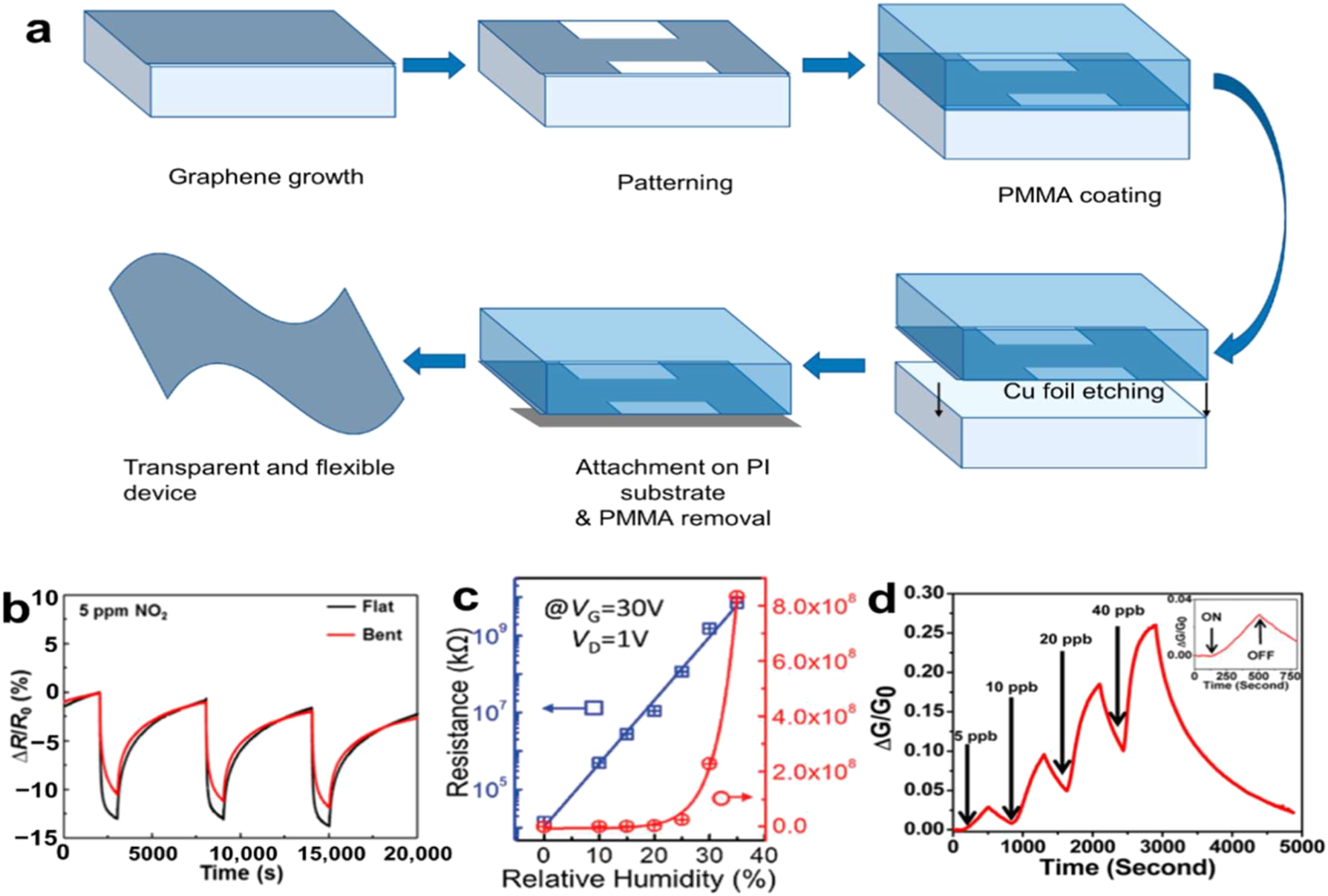
Sensing of 2D NMs. (a) Process flow diagram for gas sensor preparation. (b) Two sets of sensor response curves, one with and one without bending strain. 101 Copyright 2015, American Chemical Society. (c) Lines in blue and red, representing increase trends in linear and logarithmic coordinates, respectively, depict the resistance variation at various RHs (VG = 30 V). 102 Copyright 2017, Advanced Materials. (d) An example of a multilayer BP sensor that is sensitive to NO2 concentrations (5–40 ppb) is the relationship between the relative conductance change (ΔG/G 0) and the time in seconds. An enlarged view of a 5.0 ppb NO2 exposure response is displayed in the inset, along with the timestamps for the gas’s on and off switching. 103 Copyright 2015, American Chemical Society.
In addition, additional 2D NMs like MoS2 and black phosphorus (BP) may be used to make gas sensors with a high sensitivity by modifying the bandgap and layer count. For moisture mapping, Zhao unveiled an array of integrated humidity sensors constructed of monolayer molybdenum disulfide (ML-MoS2) that exhibited exceptionally high sensitivities. 102 In Figure 13c, we can see the MoS2 field-effect transistor’s (FET) resistance in a situation where the relative humidity is zero percent. At a gate voltage (VG) of 30 V and RH = 35 %, the resistance increases to around 8.3 1011 Ω, as compared. Because water molecules are so well adsorbed onto the carefully prepared and patterned surface of MoS2, the extremely varied resistance (more than 104 °C) is a result. By employing the gas sensor based on the black scale, Abbas et al. 103 were able to achieve a high responsivity of 2.9 % in detecting NO2 with a mass fraction as low as 5.0109. (Picture 13d). To achieve great sensitivity to tiny amounts of NO2 gas at room temperature (25 °C), Zhou et al. 106 utilized a mix of ZnO and fewer-layered MoS2Nss as sensors. The MoS2/ZnO sensors produced a response of 188 for 200 ppb NO2, a sensitivity of 0.93 ppb, and a detection limit as low as 50 ppb when they were constructed. This exceptional sensing capability is due to the hierarchical structure that is created by the synergistic combination of ZnO and MoS2 NSs, which facilitates gas diffusion, adsorption, and desorption processes.
Besides gas sensors, there are many more kinds of sensors that can profit from the special qualities of 2D NMs. The first is biosensing: 2D NMs’ huge surface areas, high conductivity, and biocompatibility make them ideal for biosensing applications such as point-of-care diagnostics, protein sensing, DNA sequencing, and biomarker detection. 107 (2) Strain and pressure sensing: 2D NMs have remarkable mechanical qualities that make them useful in strain and pressure sensing applications. The construction of flexible and wearable sensors is made possible by modifying the electrical conductivity of these materials by applying strain or pressure. 108 Chemical sensing: a great deal of research has been done on the use of 2D NMs in chemical sensing, which includes the detection of hazardous materials, heavy metals, and pollutants. They are very promising industrial safety and environmental monitoring options due to their great sensitivity and quick reaction time. 109 For example, Banerjee et al. 110 used mechanically exfoliated MoS2 NSs as channel materials and made FET sensors that could detect pH and biomolecules (Figure 14b). The protonation and deprotonation of the –OH groups on the access dielectric may have caused a change in surface charge, which is why the FET sensor displayed significant current fluctuations in response to pH changes. A biotin modification was made to the dielectric layer that covers the MoS2 channel in order to trap streptavidin, which may be used to detect biomolecules. The gating action of streptavidin’s negative charge resulted in a notable drop in current for the FET sensor when exposed. Triboelectric nanogenerators (TENGs) convert friction into electrical energy, which powers devices. There are significant medicinal uses for this. Using a thermoelectric generator (TEG), Kim et al. 111 created a portable ECG device. TEGs have the capability to produce more than 13 µW cm−2 of electrical power for more than 22 h by utilizing changes in temperature. Using magnetic Ni, Au, and 2D NMs, Nisha 3 has developed a novel sensing setup. The suggested sensor has increased sensitivity in comparison to the standard Au film-based surface plasmo resonance (SPR) detector. The optimized graphene and MoS2 layers reveal a sensitivity of 229°/RIU during angular probe analysis, leading to the desired outcome. Hassel presented a novel approach to THz radiation detection in 112 utilizing antenna-coupled mechanical resonators composed of 2D NMs that are atomically thin. The extraordinary mechanical and electrical capabilities of atomically thin graphene or 2D graphene related NMs make the proposed detectors extraordinarily sensitive.
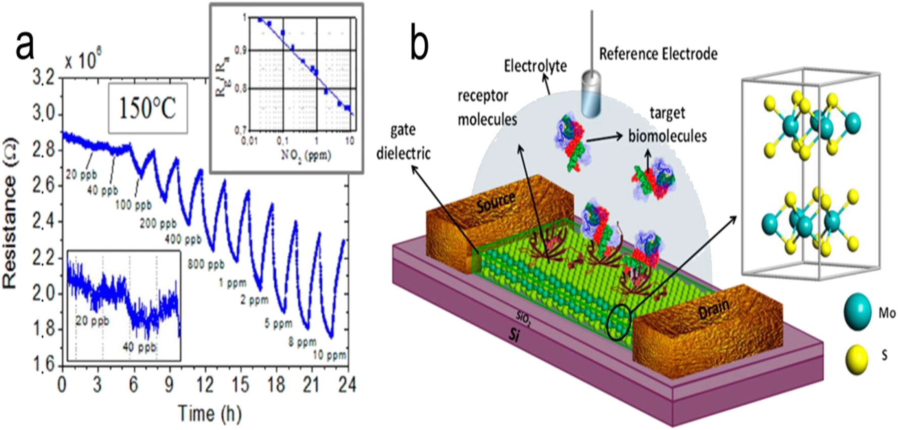
Biosensing of 2D NMs. (a) How GO reacts when the concentration of NO2 is increased at 150 °C. The main panel displays the device resistance as a function of time. The detection limit range is zoomed-in in the bottom-left inset. Sensitivity curve, top-right inset. 104 Copyright 2013, American Chemical Society. (b) Medical biosensor based on molybdenum disulfide field-effect transistor (FET) schematic. 110 Copyright 2014, ACS.
4.2 Lithium-ion battery with 2D NMs
Due to their shorter solid-state diffusion lengths, two-dimensional NMs such as MXene have garnered a lot of attention in Li-ion batteries (LIBs) since they have the potential to improve rate performance. 113 The movement of Li+ ions between the positive and negative electrodes is crucial to the operation of LIBs, a form of secondary battery, as seen in Figure 10a. So, the most important performance indicators for 2D NMs in LIBs are cycle life, internal resistance, and battery capacity (Figure 10b). 114 The materials can be used in these batteries as functional separators and anode materials due to their outstanding performance properties. In lithium-ion batteries (LIBs), the anode’s main job is to make it easier for Li+ to intercalate and deintercalated during charging and discharging, respectively. Because of their layered nature, two-dimensional NMs offer a promising channel for Li+ diffusion while preserving structural integrity through complete cycling. They are, therefore, excellent choices for anode materials. The effective preparation of bi-metallic titanium-tantalum carbide (TixTa(4x)C3) MXene was achieved by Syamsai et al. 115 When used as a Li-ion host anode, the TixTa(4x)C3 MXene had a very high reversible specific discharge Mb or Li+ they diffusion while preserving structural integrity through complete cycling. They are, therefore, excellent choices for anode materials. The effective preparation of bi-metallic titanium-tantalum carbide (TixTa(4x)C3) MXene was achieved by Syamsai et al. 115 When used as a Li-ion host anode, the TixTa(4x)C3 MXene had a very high reversible specific discharge Mb capacity of 459 mA h g−1. It also displayed a coulombic after 200 cycles, the efficiency was almost 99 %, while the capacity retention was roughly 97 %. Qian et al. 116 devised a versatile electro-deposition technique to fabricate MXene M (M = Sb, Sn, and Bi) anodes for LIBs that are durable, flexible, and self-supporting. Compared to bulk metal anodes without MXene, these hybrid anodes showed exceptional structural stability by adding the 2D MXene buffer layer. For example, during 500 cycles, the MXene Sb anode continuously retained a high reversible capacity of 516.8 mAh g−1 (Figure 15).
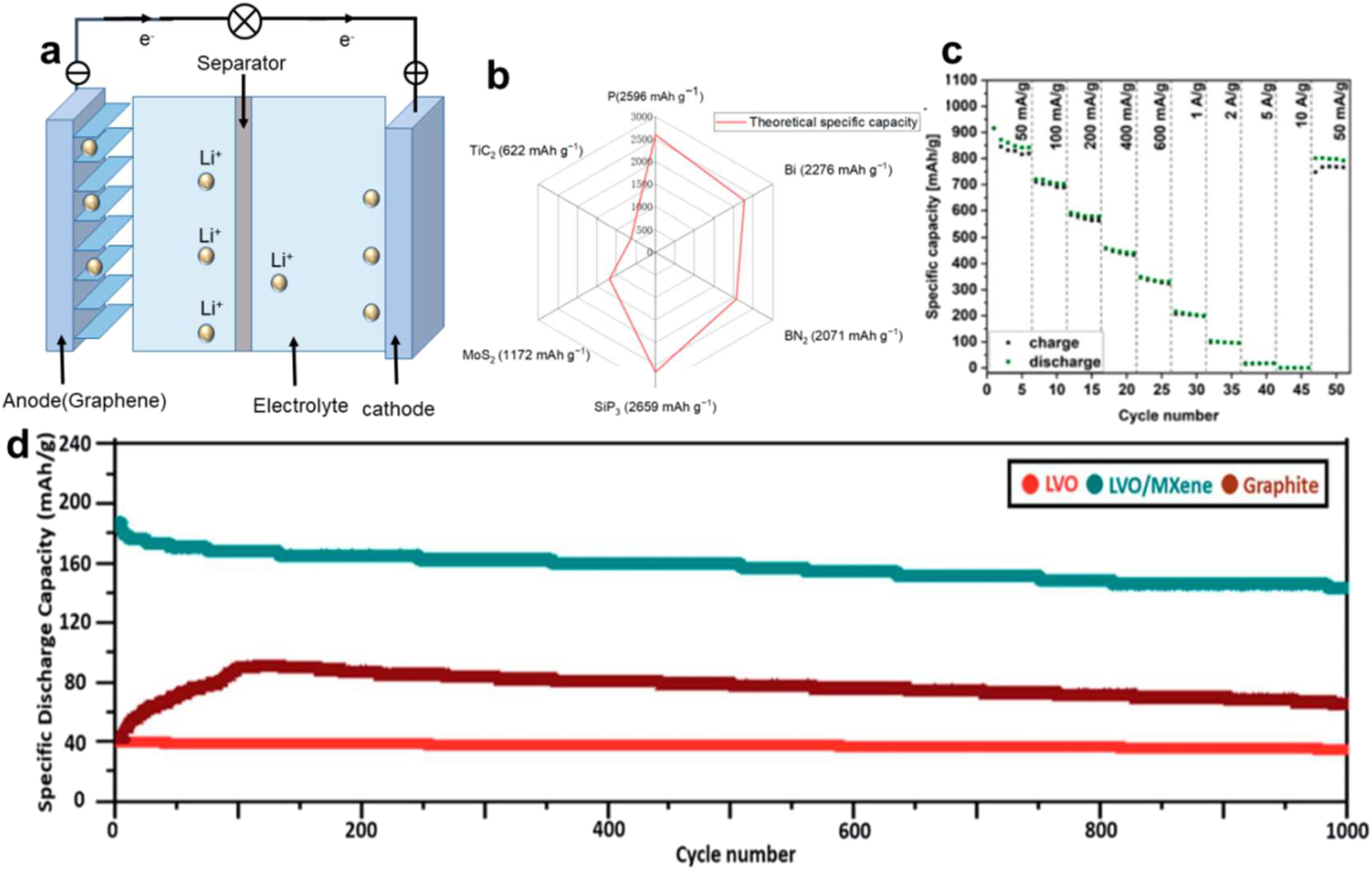
Lithium-ion battery with 2D NMs. (a) Illustrative figure of LIB work. (b) Possible unique capacities of certain two-dimensional NMs employed in LIBs. (c) Evaluation of ERGO/MoS2 films rate performance across a range of current densities. 111 Copyright 2022, Electrochimica Acta. (d) Capacity preservation below 5 C. 3 Copyright 2019, ACS.
In 2022, Keśdzierski et al. 117 created anode materials known as ERGO/MoS2, which are made up of exfoliated MoS2 (ex-MoS2) and self-expanding GO (ERGO) in a 1:1 ratio. As seen in Figure 10c, this material’s specific capacity reached 916 mA h g−1 at a current density of 50 mA g−1 and held steady at 801 mAh g−1 following 50 cycles. Huang et al. 118 created the Li3VO4 (LVO)/Ti3C2Tx composite electrode. After one charge–discharge cycle at 5 C, it shows a capacity retention of 187 mAh g−1; after 1000 cycles, it still shows a capacity decline to 146 mAh g−1. As shown in Figure 10d, compared to graphene and LVO electrodes, its performance is far better.
4.3 Photo detector with 2D NMs
Photo responsivity and detection wavelength are the two main performance factors of a photodetector, which is a device that transforms radiation from a material’s surface into an electrical signal. Graphene plasmonics has come a long way in the last few years 119 because it has unique electrical and optical properties, can be tuned, sustains long-lasting collective excitation, and tightly confines light. Aside from the absence of surface dangling bonds, two-dimensional NMs (such as BP and TMDs) offer a number of advantages, such as a large surface specific area, flatness on the atomic level, great mobility of carriers, strong interactions between matter and light, robust mechanical toughness, and efficient control of gates. They are also quite portable, which is a plus. 120 Thus, two-dimensional non-metallic semiconductors (NMs) such as graphene and transition metal dichalcogenides (TMDs) have demonstrated significant potential as fundamental components for photodetection and other optoelectronic devices. 121 Single-element 2D NMs have outstanding features, such as high mobility and a low band gap, which make them widely used in high-frequency, broad-spectrum photodetectors. 122 A unique wearable device using graphene sensitized with semiconducting quantum dots (GQD) was described by Polat et al. 123 It uses a peak responsivity of about 10−5 A W−1 at the charge neutrality point (CNP) and exhibits excellent tenability in responsivity.
Additionally, this method provides a scalable means of integrating graphene into completely flexible wearable circuitry, improving its functionality, durability, tactile perception, and outward look. The metal-graphene-metal photodetector structure (Figure 11a) by Alexander et al. 124 illustrates the ultra-short intrinsic response time of 2.1 ps at a bandwidth of 262 GHz. Graphene-based photodetectors have limited photo-responsivity, though. Arsenic (As) is one alternative single element 2D NM that can be used to solve the issues above. An ultra-wide detection range of 405 nm to 4 m was achieved by Nidhi et al. 125 using a photodetector that was made of a hybrid material consisting of black arsenic and silicon.
The detector possesses a robust spectral response (>10 A W−1) and an external quantum efficiency (>10 %) throughout the whole optical communication spectrum, as shown in Figure 11c. As a material with a direct bandgap ranging from 0.3 eV (bulk) to 2.0 eV (monolayer), BP is ideal for use in detectors operating in the visible to mid-infrared spectrum. 126 Broadband detection from visible and infrared to THz wavelengths is now within reach, thanks to the development of a BP-based high-performance top-gated phototransistor. 127 The device exhibited photovoltaic effects in the visible and infrared spectrums, as well as photo thermoelectric effects at longer wavelengths. Using frequencies between 20 and 40 GHz, the phototransistor showed a response range of 5–60 V W−1 and a low noise equivalent power (NEP) of less than 0.1 nW Hz−1/2.
On the other hand, single element 2D NMs are prone to oxidation in air and have a high chemical reactivity. On the other hand, dual element 2D NMs show better stability. 128 As a result, research into photodetectors based on dual element 2D NMs is receiving increased attention. PdSe2 can perform broadband detection because of its special characteristics. PdSe2’s bandgap narrows from 1.3 eV in a single layer to 0 eV in bulk due to its unusual pentagonal atomic structure, which depends on thickness. Outstanding ambipolar semiconducting properties, such as strong electron-apparent field-effect mobility at ambient temperature-up to 158 cm2 V−1 s−1-have been shown by the devices made with fewer layers of PdSe2. 129
Furthermore, Wu et al. 130 created PdSe2-based photodetectors that demonstrated a transmission speed of more than 2.5 Gbit s1 at a wavelength of 1550 nm, a high responsivity of 1758.7 mA W1, and an external quantum efficiency of 95 % (Figure 16d and e). WSe2 was used as a substrate passivation layer by Yang et al., 131 which improves photoresponsivity by facilitating the separation and extending the lifespan of photo-generated charge carriers. The detector performed well with a photo responsivity of 112 W A−1 and a response/decay time of 29.1/15.3 ms (Figure 11f). While the MoS2 132 photodetector displayed a positive visible photo response and a negative infrared photo response, the transistor exhibited a negative photocurrent due to the bolometric effect. The maximum responsivity of up to 105 A W−1 at 454 nm was achieved during positive photo response by combining the charge-trapping process with the photogate effect.
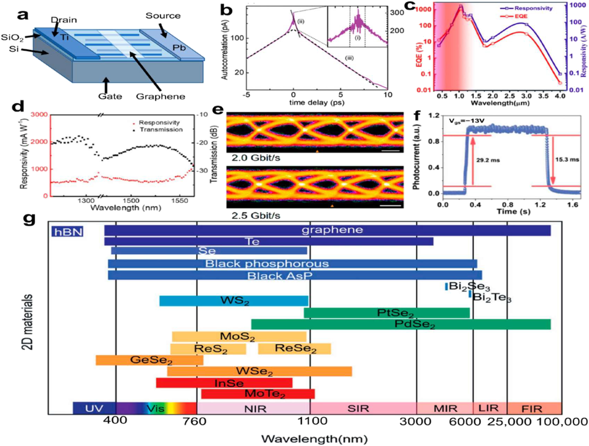
Photo detector with 2D NMs. (a) An illustration of the structure of a metal-graphene-metal photodetector. (b) Diagram of photocurrent autocorrelation signals. Interference from the pulses of the lasers causes part (i). A sub picosecond contribution is shown in part (ii) corresponding to carrier relaxation via phonons, and a picosecond contribution is shown in part (iii) tied to the photodetector’s reaction time. From (iii), we may calculate the response time by averaging the values obtained from a linear fitting approach applied to the right and left sides (dashed lines) of the autocorrelation function. 124 Copyright 2011, ACS. (c) The relationship between wavelength, photosensitivity, and maximum external quantum efficiency. 125 Copyright 2020, ACS. (d) Spectral response of photodetectors made of PdSe2. (e) The receiver eye diagram was measured using a PdSe2 photo-detector at data rates of 2.0 and 2.5 Gbit s−1. Bar scale: 200 ps. 130 Copyright 2022, ACS. (f) A PWSS-InSe device’s rise and decay curve. 131 Copyright 2022, Advanced Optical Materials. (g) Spectra of the response to partial two-dimensional materials (the lines at the bottom show distinct two-dimensional NMs, while the lines at the top show different wavelength ranges. 126 Copyright 2021, Advanced Materials.
On the other hand, it showed its maximum infrared responsivity when working in the infrared regime condition. Topological insulators’ quick and dynamic electron response to light stimulation has made them very interesting candidates for optoelectronic devices. 126 Employing Bi2Se3 flakes, a back-gated FET with an external quantum efficiency (EQE) of 233 % and a high D*(D* = √Ad/NEP) value of 3.3 × 10¹⁰ Jonesat300Kunder 1456 nm irradiation was proven effective. 133 The gadget notably attained a remarkable responsivity of 2.7 A W−1. Figure 16g displays the response spectra corresponding to partial 2D NMs (Table 3).
Nanomaterials used in various electrochemical devices.
|
Electrochemical devices |
Nano-material used |
Applications |
References |
|---|---|---|---|
| Fuel Cell | Platinum, gold, and other metal nanoparticles, MOFs, COFs, MXenes | Catalysts to improve the efficiency of electrochemical reactions that generate electricity | [134] |
| Supercapacitors | Carbon nanotubes, graphene, and other carbon-based materials, MOFs, COFs, and MXenes | Electrode materials to increase surface area, improve conductivity, and provide high power and energy densities | [135] |
| Batteries | Nanostructured metals, metal oxides, and carbon-based materials, MOFs, COFs, MXenes | Electrode materials to improve performance, increase surface area, improve conductivity, and provide higher energy and power density | [136] |
| Sensor | Metal nanoparticles, metal oxides, and carbon-based materials, MOFs, COFs, MXenes | Sensing elements to improve sensitivity and selectivity due to their high surface area, high catalytic activity, and unique optical and electrical properties | [137] |
4.4 Electromagnetic wave absorption of 2D NMs
Because two-dimensional NMs have a large specific surface area that makes it easier for electromagnetic waves to penetrate and attenuate, they display remarkable electromagnetic shielding and microwave absorption capabilities. They can thereby greatly improve reflection loss and effective absorption bandwidth. Changing the layers of 2D NMs can also change their bandgap, 138 which makes them a good choice for protecting electronic devices, communication systems, wireless identification technologies, and other uses from electromagnetic waves. Improved absorption properties and effective impedance matching are features of a graphene-builtnanomaterial for interference with electromagnetic waves developed by Ma et al. 139 At 16.8 GHz, the material receives a reflection loss of 54.1 dB, as shown in Figure 12a. In situ modification of MXene NSs with polyaniline nanorods allowed Yv et al. 140 to obtain a reflection loss of 60.6 dB at 2.6 mm material thickness (Figure 17c) and an effective absorption bandwidth of 8.64 GHz at 2.3 mm material thickness (Figure 17b).
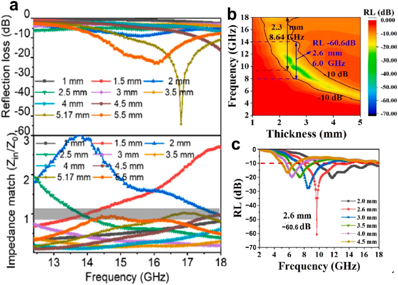
Electromagnetic wave absorption of 2D NMs. (a) Loss of impedance and identical of impedance in graphene of varying thicknesses. 139 Copyright 2022, Carbon. (b) Reflection loss and effective absorption bandwidth of MXene nanosheets. (c) MXene nanosheets’ two-dimensional RL curves. 140 Copyright 2023, Carbon.
4.5 Photocatalysis of 2D NMs
Semiconductor photocatalysis, which encompasses CO2 reduction, water splitting, photodegradation of contaminants, and other processes, has become a focus of considerable research as environmental pollution and the energy crisis increase. Surface reaction, separation/transfer, and charge carrier production are all involved in solar light-driven photocatalysis. The unique layered structure, in-plane anisotropy, variable bandgap, and ultra-high carrier mobility of 2D NMs-like C3N4 and TMDs-make them highly promising for photocatalysis applications. 141 The common insecticide nitenpyram (NTP) seriously threatens public health and environmental safety. Liu et al. 142 created a visible-light-responsive two-dimensional Bi2WO6 photocatalyst (Figure 13a) to solve this problem and used it to degrade NTP. Without a photocatalyst, NTP degradation was not discernible under visible light irradiation, as Figure 13b illustrates. The percentages of NTP degradation recorded with 2D and bulk Bi2WO6 as photocatalysts were 94.6 % and 25.4 %, respectively. 2D Bi2WO6 has significantly higher activity than bulk Bi2WO6, which is explained by its special 2D structure encouraging the separation of charge carriers produced by photosynthesis.
Moreover, photo-generated H+ and O2− are the primary active species for 2D Bi2WO6 in NTP breakdown, according to the reactive species trapping studies (Figure 18c). According to Ke et al., 143 different calcinations temperatures impacted the photocatalytic performance of g-C3N4. The sample that was calcined at 700 °C (Figure 13d) showed the topmost action for breaking down methyl orange (MO) and rhodamine B (RhB), reaching dilapidation rates of 98.81 % and 99.11 %, respectively (Figure 18e and f). Furthermore, the enhanced g-C3N4 has strong reusability. The wide surface area, effective light harvesting capability, and enhanced partition and transference of photogenerated charge carriers are made possible by the graphene-like structure, which enhances photocatalytic performance.
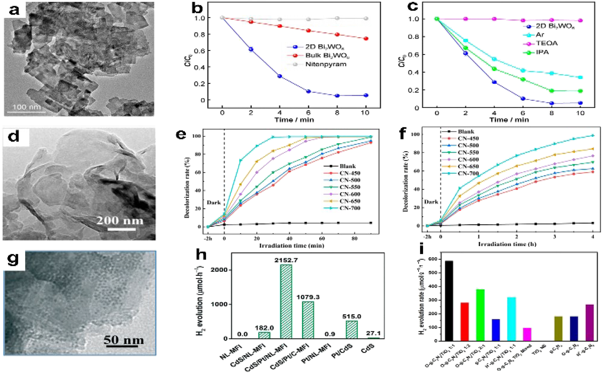
Photocatalysis of 2D NMs. (a) TEM image of 2DBi2WO6. (b) Comparison of NTP degradation curves across various samples. (c) 2D Bi2WO6 NTP degradation curves under various scavenger conditions. 122 Copyright 2022, Rare Metals. (d) TEM image of CN-700 (e) G-C3N4 (RhB) rate curve for photocatalytic decolorization. (f) Rate curve for photocatalytic decolorization of g-C3N4 (MO). 143 Copyright 2022, Catalysts. Enhancement of Pt-based catalysts. (g) TEM image of CdS/Pt/NL-MFI. (h) Rates of hydrogen evolution on various photocatalysts. 144 Copyright 2019, Catalysis Science & Technology. (i) The rates of hydrogen evolution for each photocatalyst that was tested. 145 Copyright 2017, Applied Catalysis B: Environmental.
The ideal substitute for fossil fuels would be hydrogen (H2) due to its protection, renewable nature, high energy density, and lack of ecological impact. A practical way to tackle energy and environmental concerns is by combining water splitting with photocatalysis. Therefore, it is critical to develop 2D NM-based H2 evolution catalysts. Using a 2D nanostructured porous lantern-like MFI (NL-MFI) zeolite as a support for Pt and CdS nanoparticles, Liu et al. 144 produced an effective CdS/Pt/NL-MFI photocatalyst. This is seen in Figure 17g. The CdS/Pt/NL-MFI photocatalyst showed, as expected, a notable H2 evolution rate of 2152.7 µmol h−1 when exposed to visible light (Figure 18h), thanks to an apparent quantum efficiency of 39.4 %. In comparison to the findings achieved with CdS and Pt nanoparticles supported by commercial MFI zeolite (1079.3 μmol h−1), this represents a significant improvement in the rate of H2 evolution. The NL MFI zeolite provision improves visible light absorption, assists the separation of photo generated electron–hole pairs, and promotes interactions between the photocatalyst and water molecules.
Using an in situ solvo-thermal synthetic technique, Zhong et al. 145 created a hetero-structure of graphitic C3N4/TiO2 (2D/2D O-g-C3N4/TiO2) that is covalently bonded and has a large surface area oxidized by TiO2. The resultant hybrid revealed a visible-light photocatalytic activity for H2 evolution that was 6.2 times higher than that of a physical combination of TiO2 NSs (587.1 μmol h−1 g−1) and 3.2 times higher than O-g-C3N4 (Figure 13i), in comparison to the physical combination. In this case, the charge carrier movement is facilitated by the formation of a hetero-junction by the interaction of N, O, and Ti at the interface. In addition, 2D TMDs as co-catalysts for H2 evolution have been the subject of much investigation. The efficiency of visible-light-driven H2 generation on CdS, for example, may be substantially enhanced by the addition of 2D MoSe2. 146 Chemically reducing carbon dioxide to hydrocarbons offers tremendous promise as a future technology for storing and using solar energy; it is also an integral aspect of Earth’s carbon cycle. The enhanced photocatalytic activity is usually a result of the two-dimensional photo-catalysts’ easily accessible active sites and the short electron and hole diffusion lengths to the surface. 147 The creation of ultrathin 2D porous Co3O4 catalysts (Co3O4-NS, Figure 19a and b) by air-calcining ultrathin metal-organic framework (MOF) nanosheet templates was a straightforward, scalable, and controlled process devised by Chen et al. 148 These catalysts showed remarkable stability in CO2 reduction. Figure 19c and d shows that the Co3O4-NS catalysts, when combined with a Ru-based photosensitizer and exposed to visible light, reduced CO2 more effectively than the Co3O4 bulk catalysts (Co3O4-BK). The catalytic generated CO at a rate of about 4.52 μmol h−1 and had a selectivity of 70.1 %. Co3O4-NS carries over the 2D shape and acquired porosity. The precursor MOFs allowed for electron transfer, enhanced CO2 molecule adsorption, and provided many catalytic sites for CO2 activation (Figure 20).
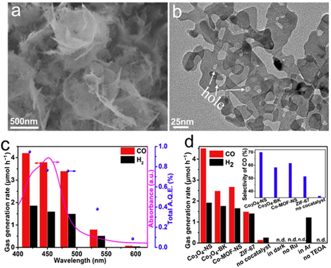
2D porous NMs. (a) SEM image and (b) TEM image of Co3O4-NS. (c) Dependent on the wavelength of CO and H2 production. The line represents the photosensor’s absorption spectra when exposed to Ru. All wavelengths’ combined AQE values are represented by the dots. (d) The change in CO and H2 levels under different response circumstances. Carbon selectivity is seen in the inset. 148 Copyright 2018, Applied Catalysis B: Environmental.
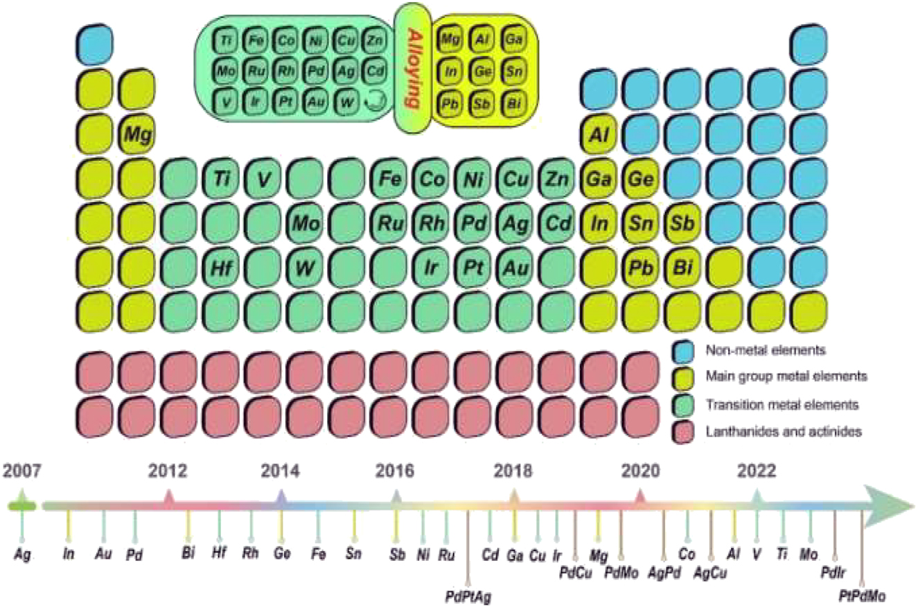
Summary and historical overview of various metallenes in the periodic table of elements. Copyright from J. Am. Chem. Soc. 139 (2017). Copyright 2023 RSC.
4.6 Electrocatalysis with 2D NMs
Future international rivalry will revolve around energy, and electrocatalysis will be essential to energy production, distribution, and use (Figure 21a). Thus, encouraging the development of electrocatalysis is essential. Certain 2D NMs, such as MOFs NSs and MXene, are widely used in electrocatalysis, as is well known. Due to its huge surface area, remarkable mechanical qualities, and excellent thermal and electrical conductivity, 2D NMs have a lot of promise for catalysis. In addition to offering a large number of active sites due to their high specific surface area, 2D NMs’ exceptional mechanical qualities also guarantee catalytic longevity. Thermal conductivity also makes effective thermal diffusion during processes possible. Furthermore, 2D NMs’ adjustable electrical characteristics provide greater catalytic stability and activity over bulk materials by allowing for control over catalytic performance. 152 , 153
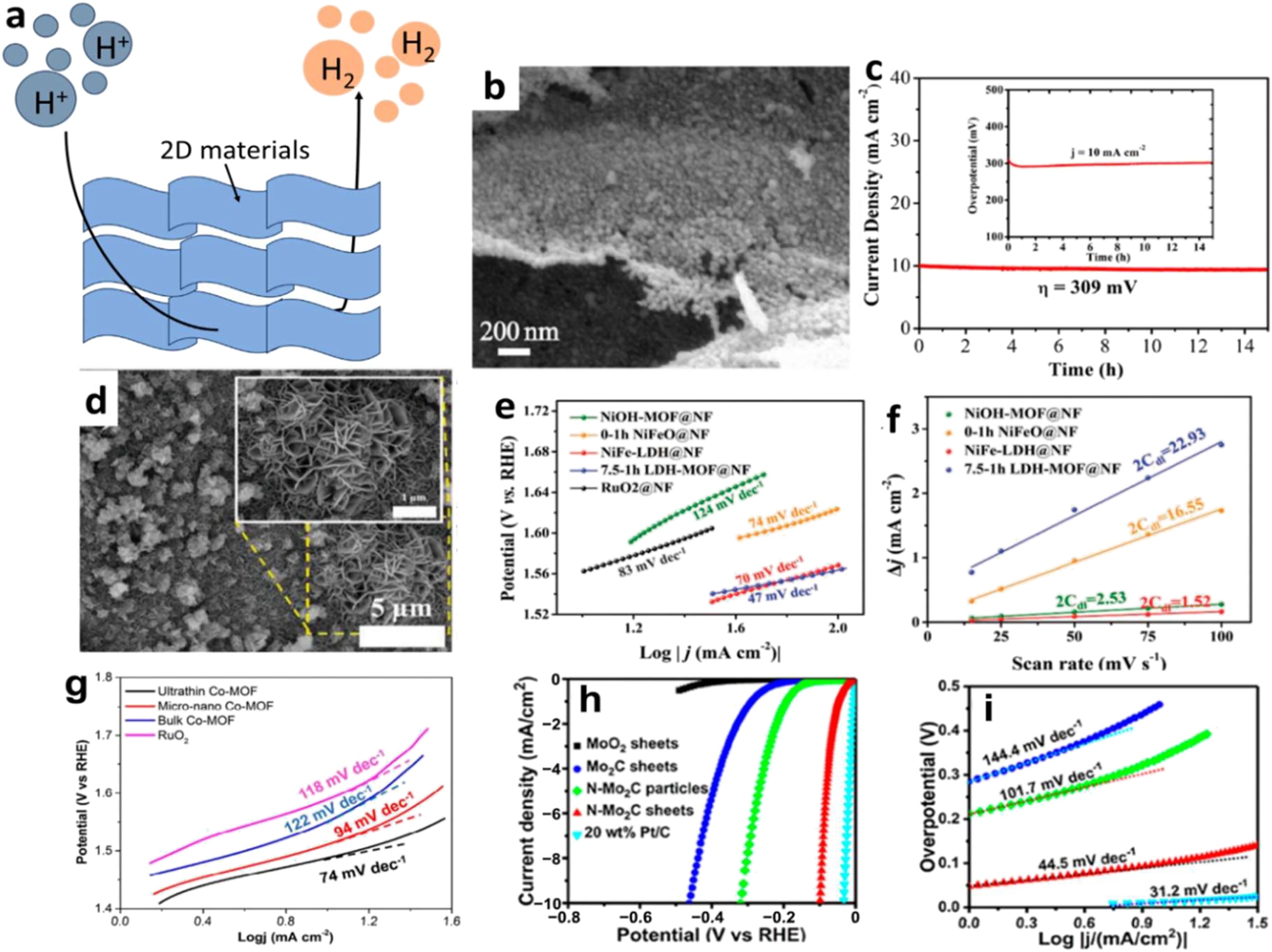
Electrocatalysis with 2D NMs. (a) A schematic depicting the process of electrocatalytic hydrogen evolution. (b) SEM images of Ni3C/NC nanoflakes. (c) The inset shows the chrono-potentiometric curve with a current density of 10 mA cm−2, while the chronoamperometry curve is at an overpotential of 309 mV. 50 Copyright 2019, Electrochimica Acta. (d) SEM pictures of pure 7.5–1 h LDH-MOF@NF. (e) Associated Tafel peaks in 1 M KOH. (f) C dl values of different samples in 1 M KOH for comparison. 149 Copyright 2019 WILEY-VCHVerlag GmbH & Co., KGaA, Weinheim. (g) Nanosheets of ultrathin 2D Co-MOFs, bulk Co-MOFs, micro-nano Co-MOFs, and RuO2. 150 Copyright 2018, Journal of Materials Chemistry A. (h) Polarization curves of several materials on the GC electrode at 5 mV s−1 in 0.5 M H2SO4, including MoO2 NSs, Mo2C NSs, N–Mo2C nanoparticles, N–Mo2C NSs, and 20 wt% Pt/C. (i) corresponding Tafel slopes from (h) Jia et al. 151 Copyright 2017, ACS Nano.
Figure 15b shows that Zheng et al. 50 created Ni3C/N-doped carbon (NC) nano-flakes with controlled structure and composition by adjusting the synthesis conditions. Figure 15c shows that the OER electrocatalytic effectiveness of the resulting Ni3C/NC nano-flakes was outstanding, with a low overpotential of 309 mV. In addition, Chen et al. 149 achieved a low Tafel slope of 47 mV dec−1 in their electrochemical oxygen evolution reaction (OER) performance by synthesizing NiFe-based MOF nanosheet arrays (LDH-MOF NS) from layered double hydroxides (LDH) (Figure 21d). These nano-sheets outperformed both RuO2 and most state-of-the-art materials.
Figure 15f shows the activators. In alkaline solutions, the bimetallic 2D MOF-Fe/Co(1:2) NSs shown outstanding electrocatalytic activity towards OER, as demonstrated by Ge. 154 Compared to bulk materials and 3D MOF-Fe/Co(1:2), their overpotential was significantly lower, measuring 238 mV at 10 mA cm−2. The improved OER activity is due to the larger surface area that is electrochemically active. Figure 21g shows that the ultrathin 2D Co-MOF NSs outperform most MOF- and Co3O4-based electrocatalysts when it comes to generating OER in alkaline solutions, as reported by Xv et al. 150 The synthesis of MXene at a low temperature of 600 °C might be enhanced by adding transition metal ions (Mo5+, W6+, and Co2+) to gelatin-based precursors, as shown by Zang et al. 155 In a two-stage process, Jia et al. 151 created N–Mo2C NSs. They detailed their exceptional HER activity, which is marked by a low overpotential (99 mV vs. RHE at 10 mA cm−2) and Tafel slope (44.5 mV dec−1), as seen in Figure 15h and i. Mo2C–Co, Mo2 xWxC, and other binary/ternary carbides/hybrids can be more easily synthesized using the proposed method. The highest performance was seen in Mo2C–Co during HER testing, with a Tafel slope of 39 mV dec−1 and an over-potential of 48 mV at a current density of 10 mA cm−2. A promising class of materials for organic electrolyte reactions (OER), transition metal nitrides (TMNs) has metallic properties that boost electrical conductivity and decrease internal potential loss. The 3 nm thick Ni3N NSs exhibited excellent OER activity with a low Tafel slope of 45 mV dec−1 in an O2–O2-saturated basic solution (1 M KOH). According to Xu et al., 156 this was disclosed.
5 Summary
Furthermore, many nanomaterials, like MXenes, are composed of naturally occurring components, which may be useful for environmentally sensitive applications that are sensitive to cost. Further research is necessary to enhance the stability and attain recyclability of 2D nanomaterial adsorbents, in order to maintain consistent performance even after repeated application. 32 , 33 , 157 – 159 To find candidate materials with improved thermal, electrical, and catalytic properties that are more suited for water treatment and environmental remediation, more research is required to close the gap between the recently anticipated and experimentally obtainable 2D nanomaterials. An essential task that could help in the creation of materials with better photocatalytic, electrocatalytic, and other beneficial features is the experimental verification of theoretical predictions. Nanomaterials are modern materials that are used in many engineering, medical and electronic applications. The most common features are described below.
Nanomaterials are distinguished from other materials that give them an increase in mechanical properties as a result of the uniform distribution of their molecules and the absence of agglomerations.
Nanomaterials are prepared in two methods are: Top-Down Method and Bottom-Up Method.
Nanomaterials are detected by several methods like (SEM, TEM, XRD, EDX, FTIR, TGA).
This study summarizes the latest research development in this topic and looks at the features of several approaches to manufacture 2D NMs. A comparison of the various methods of preparation is presented, along with a summary of the options for process optimization. Furthermore, the present applications and future perspectives for 2D NM development are discussed in this work. A summary of the creation and use of a few 2D NMs is shown in Figure 22.
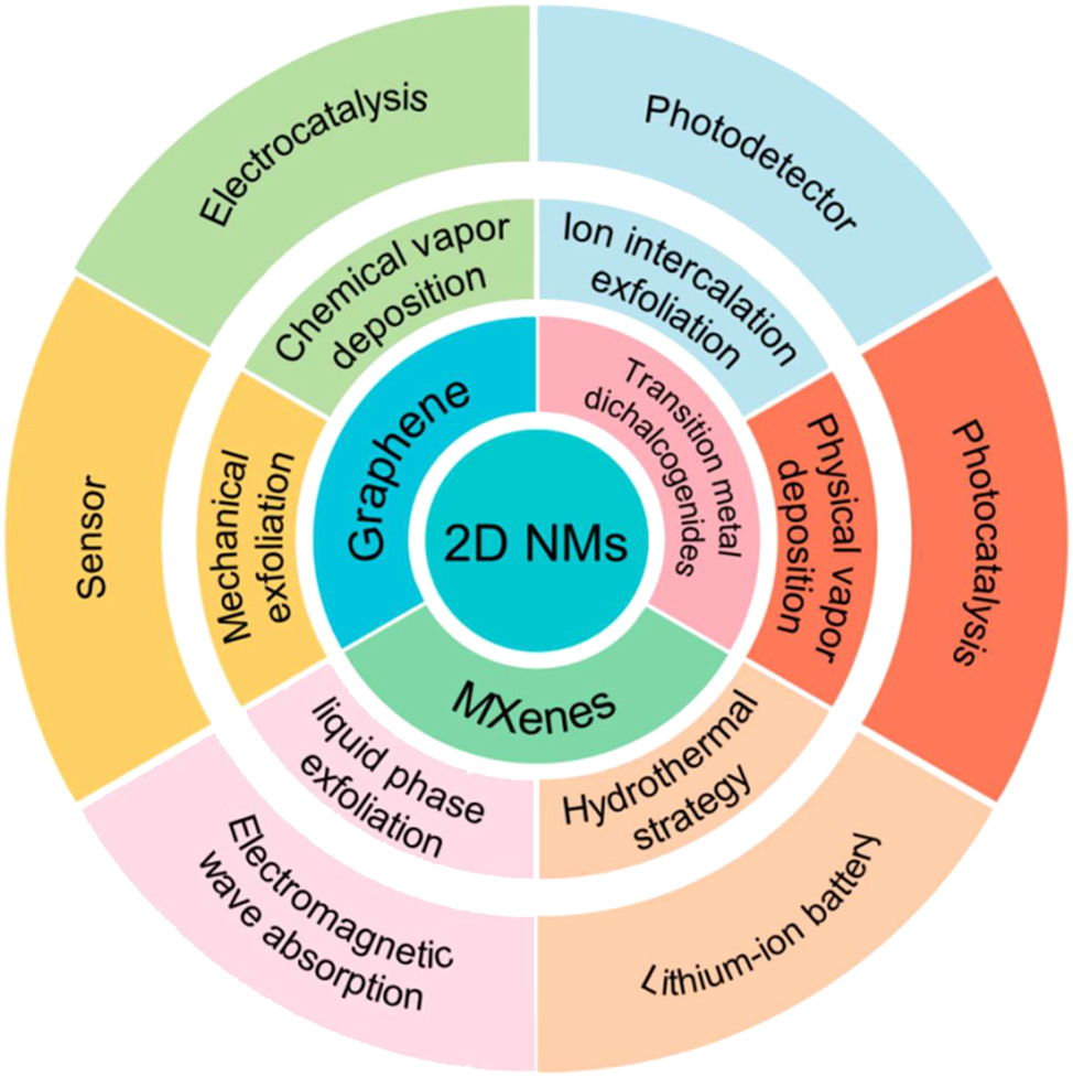
Preparation and applications of typical 2D-NMs.
5.1 Preparation of 2D NMs
Since mechanical exfoliation doesn’t include any chemical changes during preparation, it’s more cost-effective and yields more pure samples. 160 – 163 The method is not without its limitations, though, such as a lack of uniformity in sample thickness and yield. Adding adhesives or switching up the medium can make the current mechanical peeling process more efficient in manufacturing. By modifying the stripping environment to an ultra-vacuum condition, it is feasible to produce 2D NMs of superior quality that are devoid of pollutants. The size and form of 2D NMs are primarily altered by altering the solvents in the ultrasonic liquid-phase-assisted exfoliation method. The intended result may be obtained by choosing the right solvent. Nevertheless, this approach still has issues, such as low yield and a small sample size. Today, progress in ultrasonic liquid-phase-assisted exfoliation towards the synergistic use of various solvents is being made. 164 , 165
For 2D NMs NSs, the ion intercalation stripping approach shows a high yield; nevertheless, controlling the quantity of ion intercalation is still difficult. Lithium ions are currently used mostly for intercalation. The CVD technique is far more favorable than the “top-down” approach because it allows for improved manipulation and pollution avoidance during preparation. 166 – 170 There are several uses for the final product. Nevertheless, this approach has several drawbacks, including expensive expenses, unstable raw materials, and low reactant utilization rates. Currently, the main way to regulate this product is to change parameters like temperature, pressure, and distance to guarantee peak performance. Its defining features are the hydrothermal method’s ease of use, affordability, process stability, and superior product quality. Nonetheless, it still has a protracted reaction cycle and is often only used to prepare oxide products. By varying the reactor’s pH or solvent composition, fill level and other parameters, the hydrothermal process mainly regulates the shape of the products.
5.2 Applications of 2D NMs
Great electrical conductivity, huge specific surface area, stable chemical properties, and a strong propensity to adsorb gases are some of the characteristics of several 2D NMs, such as graphene and TMDs. Because of this, they show great promise for gas-sensing devices. In addition, 2D NM-based sensors can detect gases with mass fractions as low as 10−9 orders of magnitude, all while maintaining a high level of selectivity towards target gases. There has been a lot of interest in 2D NMs in LIBs because to their advantageous interactions between carriers and ions, ion diffusion pathways, and fast charge carrier transport. The retention rate and cycle life of LIBs constructed on 2D NMs are both quite high. Additionally, 2D NMs can be utilized as photo detectors with fast response times and high sensitivity due to their unique properties, which include atomic-level flatness, high carrier mobility, strong matter-light interactions, robust mechanical toughness, and gate controllability. Furthermore, these materials have no hanging bindings on their surfaces and are very portable. Conventional absorbers have a narrow absorption range and little reflection loss.
Among the well-established uses of nanomaterials are the following: UV absorbers for sun screens, synthetic bone, ferrofluids, optical fiber cladding, microelectronics, synthetic rubber, catalytic compounds, photographic supplies, inks and pigments, coatings and adhesives, and ultrafine polishing compounds. The following applications are now seeing widespread use: automotive parts, electronics, scientific instruments, sports equipment, flat panel displays, pharmaceutics, dental materials, filtration, fabrics and their treatments, surface disinfectants, diesel and fuel additives, hazardous chemical neutralizers, and flat panel displays.
Because of their special qualities, nanoparticles are thought to have a multitude of uses, ranging from environmental sciences to medical applications. There are a ton of potential for advancement in the information technology and life sciences, according to studies done by specialists in nanotechnology that map the risks and opportunities of nanotechnology. It is anticipated that medical applications, such as prostheses and early illness diagnosis and treatment, will improve our quality of life. Removal of persistent contaminants from soil and water supplies is one ecological use.
On the other hand, 2D NMs have a large specific surface area that makes it easier for electromagnetic waves to penetrate and be attenuated. They also have excellent microwave absorption and electromagnetic shielding capabilities. Therefore, adding 2D NMs may greatly improve the ability of absorbing materials to perform. In addition, 2D NMs’ distinct layered structure, in-plane anisotropy, extremely high carrier mobility, and tunable band gap provide them a great deal of potential for use in photocatalysis processes such as CO2 reduction, water splitting, and pollutant photo degradation. Furthermore, because of their vast surface area, remarkable mechanical qualities, and excellent thermal and electrical conductivity, 2D NMs are essential in electrocatalysis.
5.3 Prospect of 2D NMs
The research of 2D NM preparation and application has made substantial progress. Mechanical exfoliation is a common method for fabricating 2D NMs in both academic and industrial settings. Furthermore, CVD has the potential to produce large-area, high-quality graphene and specific TMDs, providing a solid foundation for commercialization. Second, in terms of application, the gas sensor was created using 2D NMs because of their strong gas adsorption capacity and great sensitivity to changes in the surrounding environment. Due to their remarkable chemical stability and ability to respond to visible light, 2D NMs have found extensive use in the field of photocatalysis, indicating their considerable potential for manufacture and utilization still several obstacles in the way of 2D NM research, especially in terms of preparation, where the state of the art still needs to be advanced enough to yield high-end devices. Even though mechanical exfoliation is a frequently employed technique for creating 2D NMs, its inefficiency and unpredictable sample thickness are drawbacks. Although there are many example applications for other preparation techniques, such as CVD, they are expensive and need rigorous preparation conditions. The following might be included in the future development patterns of 2D NMs: (1) the search for and analysis of new 2D NMs. Finding novel 2D NMs is a potential as the study progresses. The investigation and analysis of these novel materials will broaden the field of application and improve the 2D NMs’ performance attributes. (2) Studies on 2D NMs with several functions. Due to their special composition and characteristics, 2D NMs have many potentials uses in various industries, including electronics, sensors, catalysts, and other sectors. Research on 2D NMs will likely focus more on their development and wide range of applications in the future. (3) The development and enhancement of 2D NM preparation technique. Their preparation process significantly influences the performance and prospective applications of 2D-nanometer nanostructures. Future improvements and developments in preparation technology will result in the large-scale, controlled, and efficient manufacture of 2D NMs. (4) The extension of 2D NMs’ application area. The uses of 2D-nanometer nanometers are expected to grow with the progress of research on them, especially in fields like biology and energy. The opportunities for using 2D NMs will grow in the future and will have a significant impact on social development. In conclusion, there is still a pressing need to create new application devices, enhance the functionality of current devices, broaden the scope of applications, and completely capitalized special benefits of 2D NMs, even with the abundance of reports on the sophisticated devices and superior performance of 2D NMs in a variety of applications.
Theoretical studies of hetero-structures, surface characteristics, crystal defects, band gap control, and 2D NMs are now the main areas of interest. Because band gap management impacts the electrical characteristics of materials, it is very important. Material design and optimization are possible by effectively controlling the band gap of 2D NMs using strain, chemical modification, doping, and hetero-structures. Because a deeper comprehension of the chemical interactions, adsorption, and catalysis of materials may enhance their performance, research on surface aspects is also very important. Many 2D NMs’ surface characteristics and response processes have recently been found by researchers, opening up new possibilities and avenues for their use. Another popular issue in 2D NM research is the investigation of heterostructures and crystal defects. While heterostructures might provide new capabilities and features, crystal flaws can greatly affect the mechanical, optical, and electrical properties. Thus, it is crucial to investigate the hetero-structure and crystal defects of 2D NMs to maximize their functional design and performance. In conclusion, constant research and discovery are being done in the theoretical development of 2D NMs. Future studies will focus on improving functionality and performance to satisfy various application needs across domains.
5.4 Future prospect and of 2D NMs
The synthesis and scalability of nanomaterials is major obstacles. Because of their small size and intricate structures, nanomaterials can be difficult to synthesize and may need specialized tools and knowledge. It can be challenging to scale up the production of nanomaterials to satisfy market demands, particularly if the synthesis method is time-consuming and costly. The endurance and stability of nanoparticles present another difficulty. Over time, nanomaterials may degrade, particularly in demanding operational environments. This may reduce the dependability and lifespan of electrochemical devices made using these materials. To increase the stability and longevity of the materials, new synthesis techniques and surface modification tactics that can prevent deterioration must be developed. Additionally, nanomaterials may be poisonous or have an adverse effect on the environment. Living things can be poisoned by certain nanomaterials, especially when exposed to large concentrations. Furthermore, it is necessary to carefully assess the possible consequences of nanomaterials on ecosystems and human health because the environmental impact of these materials is yet not fully understood. Before nanomaterials may be properly employed in an electrochemical device, their toxicity and environmental impact must be thoroughly tested and evaluated. There is no one new technology that can answer the dilemma of how to apply new technology on a small scale before scaling it up for large-scale commercial use. Some of the obstacles are those related to performance, cost, safety, regulatory compliance, and reduced environmental effect.
5.4.1 Challenges and limitations of 2D nanomaterials
To comprehend the widespread application of 2D nanomaterials in water filtration, a number of obstacles must be addressed. Due to technological obstacles and production issues, 2D nanomaterials are still in their early stages of development, which makes it expensive to integrate them into industrial processes and restricts their application to small-scale structures. Significant cost savings are desired because the cost of manufacturing many 2D nanomaterials is still quite high when compared to standard products. Furthermore, it is important to take into account the 2D nanomaterial’s long-term viability in terms of both output and application. Since treating water is essentially a decontamination process, it is important to consider the biocompatibility of 2D nanomaterials in order to prevent the recontamination of substances. Low-toxicity, environmentally friendly 2D materials, such LDHs, should be given priority.
Enhancing techniques to sustain particular nanochannels with long-term operational stability would be crucial. Creating greater throughput channels is essential for high-performance solar desalination and energetic water transport. Therefore, state-of-the-art directed aggregation and self-assembly techniques that form sequence architectures with high throughput channels could be highly beneficial.
Funding source: Prince Sattam bin Abdulaziz University
Award Identifier / Grant number: PSAU/2023/R/1444
Funding source: Princess Nourah Bint Abdulrahman University
Award Identifier / Grant number: PNURSP2024R24
Acknowledgment
This research is funded by Princess Nourah Bint Abdulrahman University Researchers Supporting, Project number (PNURSP2024R24), Princess Nourah Bint Abdulrahman University, Riyadh, Saudi Arabia. This study is also supported via funding from Prince Sattam Bin Abdulaziz University project number (PSAU/2023/R/1444).
-
Research ethics: Not available.
-
Author contributions: The authors have accepted responsibility for the entire content of this manuscript and approved its submission.
-
Competing interests: All other authors state no conflict of interest.
-
Research funding: PNURSP2024R24 & PSAU/2023/R/1444.
-
Data availability: The data can be obtained on request from the corresponding author.
References
1. Saeed, M.; Marwani, H. M.; Shahzad, U.; Asiri, A. M.; Hussain, I.; Rahman, M. M. Utilizing Nanostructured Materials for Hydrogen Generation, Storage, and Diverse Applications. Chem. Asian J. 2023, e202300593.10.1002/asia.202300593Search in Google Scholar PubMed
2. Shahzad, U., Marwani, H. M., Saeed, M., Asiri, A. M., Rahman, M. M. Two-Dimensional MXenes as Emerging Materials: A Comprehensive Review. ChemistrySelect 2023, 8 (25), e202300737; https://doi.org/10.1002/slct.202300737.Search in Google Scholar
3. Nisha, A.; Maheswari, P.; Anbarasan, P. M.; Rajesh, K. B.; Jaroszewicz, Z. Sensitivity Enhancement of Surface Plasmon Resonance Sensor with 2D Material Covered Noble and Magnetic Material (Ni). Opt. Quantum Electron. 2019, 51, 1–12; https://doi.org/10.1007/s11082-018-1726-3.Search in Google Scholar
4. Obodo, R. M.; Shinde, N. M.; Chime, U. K.; Ezugwu, S.; Nwanya, A. C.; Ahmad, I.; Malik, M.; Ejikeme, P. M.; Ezema, F. I. Recent Advances in Metal Oxide/Hydroxide on Three-Dimensional Nickel Foam Substrate for High Performance Pseudocapacitive Electrodes. Curr. Opin. Electrochem. 2020, 21, 242–249; https://doi.org/10.1016/j.coelec.2020.02.022.Search in Google Scholar
5. Manzar, R.; Saeed, M.; Shahzad, U.; Al-Humaidi, J. Y.; Rehman, S. ur; Althomali, R. H.; Rahman, M. M. Recent Advancements in Boron Carbon Nitride (BNC) Nanoscale Materials for Efficient Supercapacitor Performances. Prog. Mater. Sci. 2024, 144, 101286.10.1016/j.pmatsci.2024.101286Search in Google Scholar
6. Saeed, M.; Shahzad, U.; Marwani, H. M.; Asiri, A. M.; ur Rehman, S.; Althomali, R. H.; Rahman, M. M. Recent Advancements on Sustainable Electrochemical Water Splitting Hydrogen Energy Applications Based on Nanoscale Transition Metal Oxides (TMO) Substrates. Chem. Asian J. 2024, e202301107; https://doi.org/10.1002/asia.202301107.Search in Google Scholar PubMed
7. Shahzad, U.; Saeed, M.; Rabbee, M. F.; Marwani, H. M.; Al-Humaidi, J. Y.; Altaf, M.; Althomali, R. H.; Baek, K.-H.; Awual, Md R.; Rahman, M. M. Recent Progress in Two-Dimensional Metallenes and Their Potential Application as Electrocatalyst. J. Energy Chem. 2024, 94, 577–598.10.1016/j.jechem.2024.02.068Search in Google Scholar
8. Liu, S.; Tao, H.; Zeng, Li; Qi, L.; Xu, Z.; Liu, Q.; Luo, J.-L. Shape-Dependent Electrocatalytic Reduction of CO2 to CO on Triangular Silver Nanoplates. J. Am. Chem. Soc. 2017, 139 (6), 2160–2163; https://doi.org/10.1021/jacs.6b12103.Search in Google Scholar PubMed
9. Buzea, C.; Pacheco, I. I.; Robbie, K. Nanomaterials and Nanoparticles: Sources and Toxicity. Biointerphases 2007, 2 (4), MR17–MR71; https://doi.org/10.1116/1.2815690.Search in Google Scholar PubMed
10. Donaldson, K.; Stone, V.; Tran, C. L.; Kreyling, W.; Borm, P. J. A. Nanotoxicology. Occup. Environ. Med. 2004, 61 (9), 727–728.10.1136/oem.2004.013243Search in Google Scholar PubMed PubMed Central
11. Hahn, H. Gas Phase Synthesis of Nanocrystalline Materials. Nanostruct. Mater. 1997, 9 (1–8), 3–12; https://doi.org/10.1016/s0965-9773(97)00013-5.Search in Google Scholar
12. Rao, C. N. R.; Biswas, K.; Subrahmanyam, K. S.; Govindaraj, A. Graphene, the New Nanocarbon. J. Mater. Chem. 2009, 19 (17), 2457–2469; https://doi.org/10.1039/b815239j.Search in Google Scholar
13. Reddy, G.; Reddy, S.; Swamy, B. E.; Kumar, M.; Harish, K. N.; Naveen, C. S.; Kumar, G. R.; Aravinda, T. Electrochemical Detection of Uric Acid by Using NiO Nanoparticles. Anal. Bioanal. Electrochem. 2022, 14 (4), 432–443.Search in Google Scholar
14. Shibata, S.; Aoki, K.; Yano, T.; Yamane, M. Preparation of Silica Microspheres Containing Ag Nanoparticles. J. Sol-Gel Sci. Technol. 1998, 11, 279–287; https://doi.org/10.1023/a:1008610413657.10.1023/A:1008610413657Search in Google Scholar
15. Soldano, C.; Mahmood, A.; Dujardin, E. Production, Properties and Potential of Graphene. Carbon 2010, 48 (8), 2127–2150; https://doi.org/10.1016/j.carbon.2010.01.058.Search in Google Scholar
16. Valiev, R. Nanomaterial Advantage. Nature 2002, 419 (6910), 887–889; https://doi.org/10.1038/419887a.Search in Google Scholar PubMed
17. Watson, S.; Scott, J.; Beydoun, D.; Amal, R. Studies on the Preparation of Magnetic Photocatalysts. J. Nanopart. Res. 2005, 7, 691–705; https://doi.org/10.1007/s11051-005-7520-8.Search in Google Scholar
18. Dong, L.-Xu; Chen, Q. Properties, Synthesis, and Characterization of Graphene. Front. Mater. Sci. 2010, 4, 45–51; https://doi.org/10.1007/s11706-010-0014-3.Search in Google Scholar
19. Devasahayam, S.; Hussain, C. M. Thin-Film Nanocomposite Devices for Renewable Energy Current Status and Challenges. Sustainable Mater. Technol. 2020, 26, e00233; https://doi.org/10.1016/j.susmat.2020.e00233.Search in Google Scholar
20. Serrano-Garcia, W.; Irene, B.; Guarino, V.; Thomas, S. W.; Guarino, V. New Insights to Design Electrospun Fibers with Tunable Electrical Conductive–Semiconductive Properties. Sensors 2023, 23 (3), 1606; https://doi.org/10.3390/s23031606.Search in Google Scholar PubMed PubMed Central
21. Wang, Q.; Jiang, S.; Dacheng, W. Two-dimensional Metal-organic Frameworks and Covalent Organic Frameworks. Chin. J. Chem. 2022, 40 (11), 1359–1385; https://doi.org/10.1002/cjoc.202100831.Search in Google Scholar
22. Li, C.; Wu, H.; Hong, S.; Wang, Y.; Song, N.; Han, Z.; Dong, H. 0D/2D Heterojunction Constructed by High-Dispersity Mo-Doped Ni2P Nanodots Supported on G-C3n4 Nanosheets towards Enhanced Photocatalytic H2 Evolution Activity. Int. J. Hydrogen Energy 2020, 45 (43), 22556–22566; https://doi.org/10.1016/j.ijhydene.2020.06.185.Search in Google Scholar
23. Zhang, X.; Tang, Y.; Zhang, F.; Lee, C. A Novel Aluminum-Graphite Dual-Ion Battery. Adv. Energy Mater. 2016, 6 (11), 1502588; https://doi.org/10.1002/aenm.201502588.Search in Google Scholar
24. Wang, M.; Jiang, C.; Zhang, S.; Song, X.; Tang, Y.; Cheng, H. Reversible Calcium Alloying Enables a Practical Room-Temperature Rechargeable Calcium-Ion Battery with a High Discharge Voltage. Nat. Chem. 2018, 10 (6), 667–672; https://doi.org/10.1038/s41557-018-0045-4.Search in Google Scholar PubMed
25. Zhang, C.; Chen, M.; Pan, Y.; Yang, L.; Wang, K.; Yuan, J.; Sun, Y.; Zhang, Q. Carbon Nanodots Memristor: An Emerging Candidate toward Artificial Biosynapse and Human Sensory Perception System. Adv. Sci. 2023, 10 (16), 2207229; https://doi.org/10.1002/advs.202207229.Search in Google Scholar PubMed PubMed Central
26. Abid, N.; Khan, A. M.; Shujait, S.; Chaudhary, K.; Ikram, M.; Imran, M.; Haider, J.; Khan, M.; Khan, Q.; Maqbool, M. Synthesis of Nanomaterials Using Various Top-Down and Bottom-Up Approaches, Influencing Factors, Advantages, and Disadvantages: A Review. Adv. Colloid Interface Sci. 2022, 300, 102597; https://doi.org/10.1016/j.cis.2021.102597.Search in Google Scholar PubMed
27. Awual, M. E.; Salman, Md S.; Hasan, Md M.; Hasan, Md N.; Kubra, K. T.; Sheikh, Md C.; Rasee, A. I.; Rehan, A. I.; Waliullah, R. M.; Hossain, M. S.; Marwani, H. M.; Asiri, A. M.; Rahman, M. M.; Khaleque, M. A. Ligand Imprinted Composite Adsorbent for Effective Ni (II) Ion Monitoring and Removal from Contaminated Water. J. Ind. Eng. Chem. 2024, 131, 585–592; https://doi.org/10.1016/j.jiec.2023.10.062.Search in Google Scholar
28. Kumar, N.; Salehiyan, R.; Chauke, V.; Joseph Botlhoko, O.; Setshedi, K.; Scriba, M.; Masukume, M.; Ray, S. S. Top-down Synthesis of Graphene: A Comprehensive Review. Flat Chem. 2021, 27, 100224; https://doi.org/10.1016/j.flatc.2021.100224.Search in Google Scholar
29. Sheikh, Md C.; Hasan, Md M.; Nazmul Hasan, Md; Salman, Md S.; Tul Kubra, K.; Eti Awual, M.; Waliullah, R. M.; Islam Rasee, A.; Rehan, A. I.; Hossain, M. S.; Marwani, H. M.; Khaleque, M. A.; Awual, M. R. Toxic Cadmium (II) Monitoring and Removal from Aqueous Solution Using Ligand-Based Facial Composite Adsorbent. J. Mol. Liq. 2023, 389, 122854; https://doi.org/10.1016/j.molliq.2023.122854.Search in Google Scholar
30. Hasan, Md M.; Salman, Md S.; Hasan, Md N.; Rehan, A. I.; Awual, M. E.; Rasee, A. I.; Waliullah, R. M.; Hossain, M. S.; Kubra, K. T.; Sheikh, Md C.; Khaleque, M. A.; Marwani, H. M.; Awual, M. R. Facial Conjugate Adsorbent for Sustainable Pb (II) Ion Monitoring and Removal from Contaminated Water. Colloids Surf., A 2023, 673, 131794; https://doi.org/10.1016/j.colsurfa.2023.131794.Search in Google Scholar
31. Mu, S.; Liu, Q.; Kidkhunthod, P.; Zhou, X.; Wang, W.; Tang, Y. Molecular Grafting towards High-Fraction Active Nanodots Implanted in N-Doped Carbon for Sodium Dual-Ion Batteries. Natl. Sci. Rev. 2020, 8 (7), nwaa178; https://doi.org/10.1093/nsr/nwaa178.Search in Google Scholar PubMed PubMed Central
32. Han, J.; Yue, X.; Shan, Y.; Chen, J.; Ekoya, B. G. M.; Hu, L.; Liu, R.; Qiu, Z.; Cong, C. The Effect of the Pre-strain Process on the Strain Engineering of Two-Dimensional Materials and Their Van Der Waals Heterostructures. Nanomaterials 2023c, 13 (5), 833; https://doi.org/10.3390/nano13050833.Search in Google Scholar PubMed PubMed Central
33. Zhu, Y.; Cao, X.; Tan, Y.; Wang, Y.; Hu, J.; Li, B.; Chen, Z. Single-Layer MoS2: A Two-Dimensional Material with Negative Poisson’s Ratio. Coatings 2023c, 13 (2), 283; https://doi.org/10.3390/coatings13020283.Search in Google Scholar
34. Huang, Z.; Luo, P.; Jia, S.; Zheng, H.; Lyu, Z. A Sulfur-Doped Carbon-Enhanced Na3V2(PO4)3 Nanocomposite for Sodium-Ion Storage. J. Phys. Chem. Solids 2022a, 167, 110746. https://doi.org/10.1016/j.jpcs.2022.110746.Search in Google Scholar
35. Huang, Z.; Luo, P.; Wu, Q.; Zheng, H. Constructing One-Dimensional Mesoporous Carbon Nanofibers Loaded with NaTi2(PO4)3 Nanodots as Novel Anodes for Sodium Energy Storage. J. Phys. Chem. Solids 2022b, 161, 110479. https://doi.org/10.1016/j.jpcs.2021.110479.Search in Google Scholar
36. Pan, L.; Wang, F.; He, Y.; Sun, X.; Du, G.; Zhou, Q.; Zhang, J.; Zhang, Z.; Li, J. Reassessing Self-Healing in Metallized Film Capacitors: A Focus on Safety and Damage Analysis. IEEE Trans. Dielectr. Electr. Insul. 2024; https://doi.org/10.1109/TDEI.2024.3357441.Search in Google Scholar
37. Awual, Md R. Mesoporous Composite Material for Efficient Lead (II) Detection and Removal from Aqueous Media. J. Environ. Chem. Eng. 2019, 7 (3), 103124; https://doi.org/10.1016/j.jece.2019.103124.Search in Google Scholar
38. Zhu, S.; Zhu, J.; Ye, S.; Zhang, Y.; Zhang, S.; Yang, K.; Li, M.; Zou, H.; Wang, H.; He, J. Ablation Behavior and Mechanisms of High-Entropy Rare Earth Titanates (Y0.2Gd0.2Ho0.2Er0.2Yb0.2)2Ti2O7 Coating Deposited by Plasma Spraying Technology. Surf. Coat. Technol. 2024, 478, 130414. https://doi.org/10.1016/j.surfcoat.2024.130414.Search in Google Scholar
39. Kubra, K. T.; Hasan, Md M.; Nazmul Hasan, Md; Shad Salman, Md; Abdul Khaleque, Md; Sheikh, Md C.; Rehan, A. I.; Rasee, A. I.; Waliullah, R. M.; Awual, M. E.; Hossain, M. S.; Alsukaibi, A. K.; Alshammari, H. M.; Awual, M. R. The Heavy Lanthanide of Thulium (III) Separation and Recovery Using Specific Ligand-Based Facial Composite Adsorbent. Colloids Surf., A 2023, 667, 131415; https://doi.org/10.1016/j.colsurfa.2023.131415.Search in Google Scholar
40. Wu, Y.; Wu, H.; Zhao, Y.; Jiang, G.; Shi, J.; Guo, C.; Liu, P.; Jin, Z. Metastable Structures with Composition Fluctuation in Cuprate Superconducting Films Grown by Transient Liquid-Phase Assisted Ultra-fast Heteroepitaxy. Mater. Today Nano 2023, 24, 100429. https://doi.org/10.1016/j.mtnano.2023.100429.Search in Google Scholar
41. Hasan, Md N.; Shenashen, M. A.; Hasan, Md M.; Hussein, Z.; Awual, Md R. Assessing of Cesium Removal from Wastewater Using Functionalized Wood Cellulosic Adsorbent. Chemosphere 2021, 270, 128668; https://doi.org/10.1016/j.chemosphere.2020.128668.Search in Google Scholar PubMed
42. Salman, Md S.; Sheikh, Md C.; Hasan, Md M.; Hasan, Md N.; Kubra, K. T.; Rehan, A. I.; Awual, M. E.; Rasee, A. I.; Waliullah, R. M.; Hossain, M. S.; Khaleque, M. A.; Alsukaibi, A. K.; Alshammari, H. M.; Awual, M. R. Chitosan-Coated Cotton Fiber Composite for Efficient Toxic Dye Encapsulation from Aqueous Media. Appl. Surf. Sci. 2023, 622, 157008; https://doi.org/10.1016/j.apsusc.2023.157008.Search in Google Scholar
43. Salman, Md S.; Hasan, Md N.; Hasan, Md M.; Tul Kubra, K.; Chanmiya Sheikh, Md; Islam Rehan, A.; Waliullah, R. M.; Islam Rasee, A.; Awual, M. E.; Hossain, M. S.; Alsukaibi, A. K.; Alshammari, H. M. Improving Copper (II) Ion Detection and Adsorption from Wastewater by the Ligand-Functionalized Composite Adsorbent. J. Mol. Struct. 2023, 1282, 135259; https://doi.org/10.1016/j.molstruc.2023.135259.Search in Google Scholar
44. Yang, S.; Zhang, Y.; Sha, Z.; Huang, Z.; Wang, H.; Wang, F.; Li, J. Deterministic Manipulation of Heat Flow via Three-Dimensional-Printed Thermal Meta-Materials for Multiple Protection of Critical Components. ACS Appl. Mater. Interfaces 2022, 14 (34), 39354–39363; https://doi.org/10.1021/acsami.2c09602.Search in Google Scholar PubMed
45. Hasan, Md N.; Salman, Md S.; Hasan, Md M.; Tul Kubra, K.; Sheikh, Md C.; Islam Rehan, A.; Rasee, A. I.; Awual, M. E.; Waliullah, R. M.; Hossain, M. S.; Khandaker, S.; Alsukaibi, A. K.; Alshammari, H. M.; Awual, M. R. Assessing Sustainable Lutetium (III) Ions Adsorption and Recovery Using Novel Composite Hybrid Nanomaterials. J. Mol. Struct. 2023, 1276, 134795; https://doi.org/10.1016/j.molstruc.2022.134795.Search in Google Scholar
46. Zhao, X.; Fan, B.; Qiao, N.; Soomro, R. A.; Zhang, R.; Xu, B. Stabilized Ti3C2Tx-Doped 3D Vesicle Polypyrrole Coating for Efficient Protection toward Copper in Artificial Seawater. Appl. Surf. Sci. 2024, 642, 158639. https://doi.org/10.1016/j.apsusc.2023.158639.Search in Google Scholar
47. Awual, Md R.; Hasan, Md M. A Ligand Based Innovative Composite Material for Selective Lead (II) Capturing from Wastewater. J. Mol. Liq. 2019, 294, 111679; https://doi.org/10.1016/j.molliq.2019.111679.Search in Google Scholar
48. Guan, S.; Zhou, J.; Sun, S.; Peng, Q.; Guo, X.; Liu, B.; Zhou, X.; Tang, Y. Nonmetallic Se/N Co-Doped Amorphous Carbon Anode Collaborates to Realize Ultra-High Capacity and Fast Potassium Storage for Potassium Dual-Ion Batteries. Adv. Funct. Mater. 2024, 2314890. https://doi.org/10.1002/adfm.202314890.Search in Google Scholar
49. Shahat, A.; Khadiza, T. K.; El-marghany, A. Equilibrium, Thermodynamic and Kinetic Modeling of Triclosan Adsorption on Mesoporous Carbon Nanosphere: Optimization Using Box-Behnken Design. J. Mol. Liq. 2023, 383, 122166; https://doi.org/10.1016/j.molliq.2023.122166.Search in Google Scholar
50. Hao, J.; Zhang, G.; Zheng, Y.; Luo, W.; Jin, C.; Wang, R.; Wang, Z.; Zheng, W. Controlled Synthesis of Ni3C/Nitrogen-Doped Carbon Nanoflakes for Efficient Oxygen Evolution. Electrochim. Acta 2019, 320, 134631; https://doi.org/10.1016/j.electacta.2019.134631.Search in Google Scholar
51. Hao, S.; Zhao, X.; Cheng, Q.; Xing, Y.; Ma, W.; Wang, X.; Zhao, G.; Xu, X. A Mini Review of the Preparation and Photocatalytic Properties of Two-Dimensional Materials. Front. Chem. 2020, 8, 582146; https://doi.org/10.3389/fchem.2020.582146.Search in Google Scholar PubMed PubMed Central
52. Sharma, A.; Rangra, V. S.; Thakur, A. Synthesis, Properties, and Applications of MBenes (Two-Dimensional Metal Borides) as Emerging 2D Materials: A Review. J. Mater. Sci. 2022, 57 (27), 12738–12751; https://doi.org/10.1007/s10853-022-07378-3.Search in Google Scholar
53. Huang, G.; Jiang, P.; Zhang, X.; Zhou, C.; Zhou, J.; Huang, Y.; Yang, P.; Yang, L.; Tian, X.; Yue, H. Efficient Preparation and Characterization of Graphene Based on Ball Milling. Diamond Relat. Mater. 2022, 130, 109438; https://doi.org/10.1016/j.diamond.2022.109438.Search in Google Scholar
54. Sun, Z.; Han, X.; Cai, Z.; Yue, S.; Geng, D.; Rong, D.; Zhao, L.; Zhang, Y.-Q.; Peng, C.; Chen, L.; Zhou, X.; Huang, Y.; Wu, K.; Feng, B. Exfoliation of 2D Van Der Waals Crystals in Ultrahigh Vacuum for Interface Engineering. Sci. Bull. 2022, 67 (13), 1345–1351; https://doi.org/10.1016/j.scib.2022.05.017.Search in Google Scholar PubMed
55. An, L.; Yu, Y.; Bai, C.; Bai, Y.; Zhang, B.; Gao, K.; Wang, X.; Lai, Z.; Zhang, J. Simultaneous Production and Functionalization of Hexagonal Boron Nitride Nanosheets by Solvent-free Mechanical Exfoliation for Superlubricant Water-Based Lubricant Additives. npj 2D Mater. Appl. 2019, 3 (1), 28; https://doi.org/10.1038/s41699-019-0111-9.Search in Google Scholar
56. Deng, S.; Che, S.; Debbarma, R.; Berry, V. Strain in a Single Wrinkle on an MoS 2 Flake for In-Plane Realignment of Band Structure for Enhanced Photo-Response. Nanoscale 2019, 11 (2), 504–511; https://doi.org/10.1039/c8nr05884a.Search in Google Scholar PubMed
57. Kim, S. Y.; Kim, S.-I.; Kim, M. K.; Kim, J.; Mizusaki, S.; Ko, D.-S.; Jung, C.; Yun, D.-J.; Jong, W. R.; Kim, H.-S.; Sohn, H.; Lim, J. H.; Oh, J. M.; Jeong, H. M.; Shin, W. H. Ultrasonic Assisted Exfoliation for Efficient Production of RuO 2 Monolayer Nanosheets. Inorg. Chem. Front. 2021, 8 (20), 4482–4487, https://doi.org/10.1039/d1qi00652e.Search in Google Scholar
58. Mushfiq, S. W.; Afzalzadeh, R. Verification of Experimental Results with Simulation on Production of Few-Layer Graphene by Liquid-phase Exfoliation Utilizing Sonication. Sci. Rep. 2022, 12 (1), 9872; https://doi.org/10.1038/s41598-022-10971-w.Search in Google Scholar PubMed PubMed Central
59. Qi, X.; Ding, C.; Gao, M.; Wang, F.; Hui, Y.; Yao, Y.; Qu, R.; Guo, Y.; Zhang, Z.; Zhao, W.; Xing, H. High-Efficient Production of Mono-To Few-Layer GaSe Nanosheets via a Novel Na2CO3-Promoted Ultrasonic Exfoliation Method. Mater. Lett. 2021, 305, 130747; https://doi.org/10.1016/j.matlet.2021.130747.Search in Google Scholar
60. Shi, D.; Yang, M.; Chang, B.; Ai, Z.; Zhang, K.; Shao, Y.; Wang, S.; Wu, Y.; Xiaopeng, H. Ultrasonic-Ball Milling: A Novel Strategy to Prepare Large-Size Ultrathin 2D Materials. Small 2020, 16 (13), 1906734; https://doi.org/10.1002/smll.201906734.Search in Google Scholar PubMed
61. Tyurnina, A. V.; Morton, J. A.; Kaur, A.; Mi, J.; Grobert, N.; Porfyrakis, K.; Tzanakis, I.; Eskin, D. G. Effects of Green Solvents and Surfactants on the Characteristics of Few-Layer Graphene Produced by Dual-Frequency Ultrasonic Liquid Phase Exfoliation Technique. Carbon 2023, 206, 7–15; https://doi.org/10.1016/j.carbon.2023.01.062.Search in Google Scholar
62. Wang, J.; Zhang, Y.; Liua, G.; Zhang, T.; Zhang, C.; Zhang, Y.; Feng, Y.; Chi, Q. Improvements in the Magnesium Ion Transport Properties of Graphene/CNT-Wrapped TiO2-B Nanoflowers by Nickel Doping. Small 2023, 20, e2304969; https://doi.org/10.1002/smll.202304969.Search in Google Scholar PubMed
63. Lin, Z.; Wang, C.; Yang, C. Emerging Group-VI Elemental 2D Materials: Preparations, Properties, and Device Applications. Small 2020, 16 (41), 2003319; https://doi.org/10.1002/smll.202003319.Search in Google Scholar PubMed
64. Xie, L.; Li, H.; Yang, Z.; Zhao, X.; Zhang, H.; Zhang, P.; Cao, Z.; He, J.; Peng, P.; Liu, J.; Wei, J.; Song, D.; Qi, W. Facile Large-Scaled Fabrication of Graphene-like Materials by Ultrasonic Assisted Shear Exfoliation Method for Enhanced Performance on Flexible Supercapacitor Applications. Appl. Nanosci. 2020, 10, 1131–1139; https://doi.org/10.1007/s13204-019-01189-w.Search in Google Scholar
65. Wang, J.; Pan, Z.; Wang, Y.; Wang, L.; Su, L.; Cuiuri, D.; Zhao, Y.; Li, H. Evolution of Crystallographic Orientation, Precipitation, Phase Transformation and Mechanical Properties Realized by Enhancing Deposition Current for Dual-Wire Arc Additive Manufactured Ni-Rich NiTi Alloy. Addit. Manuf. 2020, 34, 101240. https://doi.org/10.1016/j.addma.2020.101240.Search in Google Scholar
66. Takahashi, Y.; Kobayashi, Y.; Wang, Z.; Ito, Y.; Ota, M.; Ida, H.; Kumatani, A.; Miyazawa, K.; Fujita, T.; Shiku, H.; Korchev, Y. E.; Miyata, Y.; Fukuma, T.; Chen, M.; Matsue, T. High-Resolution Electrochemical Mapping of the Hydrogen Evolution Reaction on Transition-Metal Dichalcogenide Nanosheets. Angew. Chem., Int. Ed. 2020, 59 (9), 3601–3608; https://doi.org/10.1002/anie.201912863.Search in Google Scholar PubMed
67. El Garah, M.; Bertolazzi, S.; Ippolito, S.; Eredia, M.; Janica, I.; Melinte, G.; Ersen, O.; Marletta, G.; Ciesielski, A.; Samorì, P. MoS2 Nanosheets via Electrochemical Lithium-Ion Intercalation under Ambient Conditions. FlatChem 2018, 9, 33–39; https://doi.org/10.1016/j.flatc.2018.06.001.Search in Google Scholar
68. Xu, Z.; Zhang, Y.; Liu, M.; Meng, Q.; Shen, C.; Xu, L.; Zhang, G.; Gao, C. Two-Dimensional Titanium Carbide MXene Produced by Ternary Cations Intercalation via Structural Control with Angstrom-Level Precision. Iscience 2022, 25 (12), 105562; https://doi.org/10.1016/j.isci.2022.105562.Search in Google Scholar PubMed PubMed Central
69. Tian, Li; Qiao, H.; Huang, Z.; Xiang, Q. Li-Ion Intercalated Exfoliated WS2 Nanosheets with Enhanced Electrocatalytic Hydrogen Evolution Performance. Cryst. Res. Technol. 2021, 56 (4), 2000165; https://doi.org/10.1002/crat.202000165.Search in Google Scholar
70. Hou, X.; Zhang, W.; Peng, J.; Zhou, L.; Wu, J.; Xie, K.; Fang, Z. Phase Transformation of 1T′-MoS2 Induced by Electrochemical Prelithiation for Lithium-Ion Storage. ACS Appl. Energy Mater. 2022, 5 (9), 11292–11303; https://doi.org/10.1021/acsaem.2c01835.Search in Google Scholar
71. Peng, R.; Ma, Y.; Wu, Q.; Huang, B.; Dai, Y. Two-Dimensional Materials with Intrinsic Auxeticity: Progress and Perspectives. Nanoscale 2019, 11 (24), 11413–11428; https://doi.org/10.1039/c9nr03546j.Search in Google Scholar PubMed
72. Xu, P.; Liu, X.; Zhao, Y.; Lan, D.; Shin, I. Study of Graphdiyne Biomimetic Nanomaterials as Fluorescent Sensors of Ciprofloxacin Hydrochloride in Water Environment. Desalin. Water Treat. 2023, 302, 129–137; https://doi.org/10.5004/dwt.2023.29723.Search in Google Scholar
73. Yi, K.; Liu, D.; Chen, X.; Yang, J.; Wei, D.; Liu, Y.; Wei, D. Plasma-Enhanced Chemical Vapor Deposition of Two-Dimensional Materials for Applications. Acc. Chem. Res. 2021, 54 (4), 1011–1022; https://doi.org/10.1021/acs.accounts.0c00757.Search in Google Scholar PubMed
74. Chen, L.; Yang, C.; Yan, C. High-Performance UV Detectors Based on 2D CVD Bismuth Oxybromide Single-Crystal Nanosheets. J. Mater. Sci. Technol. 2020, 48, 100–104; https://doi.org/10.1016/j.jmst.2020.03.008.Search in Google Scholar
75. Zhang, Z.; Xu, X.; Song, J.; Gao, Q.; Li, S.; Hu, Q.; Li, X.; Wu, Y. High-Performance Transistors Based on Monolayer CVD MoS2 Grown on Molten Glass. Appl. Phys. Lett. 2018, 113 (20), 202103; https://doi.org/10.1063/1.5051781.Search in Google Scholar
76. Chen, Z.; Xie, C.; Wang, W.; Zhao, J.; Liu, B.; Shan, J.; Wang, X.; Hong, M.; Lin, L.; Huang, L.; Lin, X.; Yang, S.; Gao, X.; Zhang, Y.; Gao, P.; Novoselov, K. S.; Sun, J.; Liu, Z. Direct Growth of Wafer-Scale Highly Oriented Graphene on Sapphire. Sci. Adv. 2021, 7 (47), eabk0115; https://doi.org/10.1126/sciadv.abk0115.Search in Google Scholar PubMed PubMed Central
77. Li, J.; Chen, M.; Zhang, C.; Dong, H.; Lin, W.; Zhuang, P.; Wen, Y.; Tian, B.; Cai, W.; Zhang, X. Fractal-theory-based Control of the Shape and Quality of CVD‐grown 2D Materials. Adv. Mater. 2019, 31 (35), 1902431; https://doi.org/10.1002/adma.201902431.Search in Google Scholar PubMed
78. Tang, L.; Tang, B.; Zhang, H.; Yuan, Y. Review of Research on AlGaN MOCVD Growth. ECS J. Solid State Sci. Technol. 2020, 9 (2), 024009; https://doi.org/10.1149/2162-8777/ab6833.Search in Google Scholar
79. Noh, G.; Song, H.; Choi, H.; Kim, M.; Jeong, J. H.; Lee, Y.; Choi, M.-Y.; Oh, S.; Jo, M.-K.; Woo, D. Y.; Jo, Y.; Park, E.; Moon, E.; Kim, T. S.; Chai, H.; Huh, W.; Lee, C.; Kim, C.; Yang, H.; Song, S.; Jeong, H. Y.; Lee, G.; Lim, J.; Kim, C. G.; Chung, T.; Kwak, J. Y.; Kang, K. Large Memory Window of Van Der Waals Heterostructure Devices Based on MOCVD-Grown 2D Layered Ge4Se9. Adv. Mater. 2022, 34 (41), 2204982; https://doi.org/10.1002/adma.202204982.Search in Google Scholar PubMed
80. Li, Y.; Jeffrey, D. C.; Hanson, E. D.; Murthy, A. A.; Shiqiang, H.; Shi, F.; Li, Q.; Wolverton, C.; Chen, X.; Dravid, V. P. Au@ MoS2 Core–Shell Heterostructures with Strong Light–Matter Interactions. Nano Lett. 2016, 16 (12), 7696–7702; https://doi.org/10.1021/acs.nanolett.6b03764.Search in Google Scholar PubMed
81. Muratore, C.; Voevodin, A. A.; Glavin, N. R. Physical Vapor Deposition of 2D Van Der Waals Materials: A Review. Thin Solid Films 2019, 688, 137500; https://doi.org/10.1016/j.tsf.2019.137500.Search in Google Scholar
82. Anbalagan, A. K.; Hu, F.-C.; Chan, W. K.; Chhaganlal Gandhi, A.; Gupta, S.; Chaudhary, M.; Chuang, K.-W.; Ramesh, A. K.; Billo, T.; Sabbah, A.; Chiang, C. Y.; Tseng, Y. C.; Chueh, Y. L.; Wu, S. Y.; Tai, N. H.; Chen, H. Y. T.; Lee, C. H. Gamma-Ray Irradiation Induced Ultrahigh Room-Temperature Ferromagnetism in MoS2 Sputtered Few-Layered Thin Films. ACS Nano 2023, 17 (7), 6555–6564; https://doi.org/10.1021/acsnano.2c11955.Search in Google Scholar PubMed
83. Mannix, A. J.; Zhou, X.-F.; Kiraly, B.; Wood, J. D.; Alducin, D.; Myers, B. D.; Liu, X.; Fisher, B. L.; Santiago, U.; Guest, J. R.; Yacaman, M. J.; Ponce, A.; Oganov, A. R.; Hersam, M. C.; Guisinger, N. P. Synthesis of Borophenes: Anisotropic, Two-Dimensional Boron Polymorphs. Science 2015, 350 (6267), 1513–1516; https://doi.org/10.1126/science.aad1080.Search in Google Scholar PubMed PubMed Central
84. Zhang, X.; Zhang, Y.; Yu, B.-B.; Yin, X.-L.; Jiang, W.-J.; Jiang, Y.; Hu, J.-S.; Wan, L.-J. Physical Vapor Deposition of Amorphous MoS2 Nanosheet Arrays on Carbon Cloth for Highly Reproducible Large-Area Electrocatalysts for the Hydrogen Evolution Reaction. J. Mater. Chem. A 2015, 3 (38), 19277–19281; https://doi.org/10.1039/c5ta05793k.Search in Google Scholar
85. Zhu, F.-F.; Chen, W.-J.; Xu, Y.; Gao, C.-L.; Guan, D.-D.; Liu, C.-H.; Qian, D.; Zhang, S.-C.; Jia, J.-F. Epitaxial Growth of Two-Dimensional Stanene. Nat. Mater. 2015, 14 (10), 1020–1025; https://doi.org/10.1038/nmat4384.Search in Google Scholar PubMed
86. Ji, J.; Song, X.; Liu, J.; Yan, Z.; Huo, C.; Zhang, S.; Su, M.; Liao, L.; Wang, W.; Ni, Z.; Hao, Y.; Zeng, H. Two-Dimensional Antimonene Single Crystals Grown by Van Der Waals Epitaxy. Nat. Commun. 2016, 7 (1), 13352; https://doi.org/10.1038/ncomms13352.Search in Google Scholar PubMed PubMed Central
87. Liu, Z.; Wei, W.; Xu, K.; Wu, H.; Su, T.; Zhu, Y.; Wang, Z. Preparation and Electrochromic Properties of Vanadium Oxide Two-Dimensional Materials. Mater. Res. Express 2019, 6 (11), 1150a1; https://doi.org/10.1088/2053-1591/ab4b87.Search in Google Scholar
88. Pradhan, I.; Bandyopadhyay, A.; Nayak, A.; Kumar, P. Freestanding Silver-Doped Zinc Oxide 2D Crystals Synthesized by a Surface Energy-Controlled Hydrothermal Strategy. ACS Appl. Nano Mater. 2021, 4 (10), 10534–10544; https://doi.org/10.1021/acsanm.1c02046.Search in Google Scholar
89. Huang, B.; Liu, Y.; Xie, Z. Biomass Derived 2D Carbons via a Hydrothermal Carbonization Method as Efficient Bifunctional ORR/HER Electrocatalysts. J. Mater. Chem. A 2017, 5 (45), 23481–23488; https://doi.org/10.1039/c7ta08052b.Search in Google Scholar
90. Long, Le N.; Quang, N. T.; Tung Khuong, T.; Kien, P. T.; Nguyen, H. T.; Tran, V. K. Controllable Synthesis by Hydrothermal Method and Optical Properties of 2D MoS2/RGO Nanocomposites. J. Sol-Gel Sci. Technol. 2023, 106 (3), 699–714; https://doi.org/10.1007/s10971-023-06072-3.Search in Google Scholar
91. Vidhya, M.; Selvakumari, T. M.; Marnadu, R.; Ashraf, I. M.; Shkir, M. Impact of Temperature on the Properties of MoS2 Nanoflakes Synthesized by Facile Hydrothermal Method for Electrochemical Supercapacitor Applications. Inorg. Chem. Commun. 2022, 145, 109928; https://doi.org/10.1016/j.inoche.2022.109928.Search in Google Scholar
92. Schilirò, E.; Lo Nigro, R.; Roccaforte, F.; Giannazzo, F. Substrate-Driven Atomic Layer Deposition of High-κ Dielectrics on 2D Materials. Appl. Sci. 2021, 11 (22), 11052; https://doi.org/10.3390/app112211052.Search in Google Scholar
93. Martella, C.; Melloni, P.; Cinquanta, E.; Cianci, E.; Alia, M.; Longo, M.; Lamperti, A.; Vangelista, S.; Fanciulli, M.; Molle, A. Engineering the Growth of MoS2 via Atomic Layer Deposition of Molybdenum Oxide Film Precursor. Adv. Electron. Mater. 2016, 2 (10), 1600330; https://doi.org/10.1002/aelm.201600330.Search in Google Scholar
94. Tan, C.; Cao, X.; Wu, X.-J.; He, Q.; Yang, J.; Zhang, X.; Chen, J.; Zhao, W.; Han, S.; Nam, G.-H.; Sindoro, M.; Zhang, H. Recent Advances in Ultrathin Two-Dimensional Nanomaterials. Chem. Rev. 2017, 117 (9), 6225–6331; https://doi.org/10.1021/acs.chemrev.6b00558.Search in Google Scholar PubMed
95. Yang, T.; Xu, C.; Liu, C.; Ye, Y.; Sun, Z.; Wang, B.; Luo, Z. Conductive Polymer Hydrogels Crosslinked by Electrostatic Interaction with PEDOT: PSS Dopant for Bioelectronics Application. Chem. Eng. J. 2022, 429, 132430; https://doi.org/10.1016/j.cej.2021.132430.Search in Google Scholar
96. Yin, P. T.; Shah, S.; Chhowalla, M.; Lee, K.-B. Design, Synthesis, and Characterization of Graphene–Nanoparticle Hybrid Materials for Bioapplications. Chem. Rev. 2015, 115 (7), 2483–2531; https://doi.org/10.1021/cr500537t.Search in Google Scholar PubMed PubMed Central
97. Li, B. L.; Inggrid Setyawati, M.; Lin Zou, H.; Jiang, X. D.; Luo, H. Q.; Li, N. B.; Leong, D. T. Emerging 0D Transition-Metal Dichalcogenides for Sensors, Biomedicine, and Clean Energy. Small 2017, 13 (31), 1700527; https://doi.org/10.1002/smll.201700527.Search in Google Scholar PubMed
98. Rajesh, D.; Francis, M. K.; Balaji Bhargav, P.; Nafis, A.; Balaji, C. 2D Layered Nickel-Cobalt Double Hydroxide Nano Sheets@ 1D Silver Nanowire-Graphitic Carbon Nitrides for High Performance Super Capacitors. J. Alloys Compd. 2022, 898, 162803; https://doi.org/10.1016/j.jallcom.2021.162803.Search in Google Scholar
99. Glavin, N. R.; Rao, R.; Varshney, V.; Bianco, E.; Apte, A.; Roy, A.; Ringe, E.; Ajayan, P. M. 2D Materials: Emerging Applications of Elemental 2D Materials (Adv. Mater. 7/2020). Adv. Mater. 2020, 32 (7), 2070052; https://doi.org/10.1002/adma.202070052.Search in Google Scholar
100. Varghese, S. S.; Hanna Varghese, S.; Swaminathan, S.; Singh, K. K.; Mittal, V. Two-Dimensional Materials for Sensing: Graphene and beyond. Electronics 2015, 4 (3), 651–687; https://doi.org/10.3390/electronics4030651.Search in Google Scholar
101. Kim, Y. H.; Kim, S. J.; Kim, Y.-J.; Shim, Y.-S.; Kim, S. Y.; Hong, B. H.; Jang, Ho W. Self-Activated Transparent All-Graphene Gas Sensor with Endurance to Humidity and Mechanical Bending. ACS Nano 2015, 9 (10), 10453–10460; https://doi.org/10.1021/acsnano.5b04680.Search in Google Scholar PubMed
102. Zhao, J.; Li, N.; Hua, Y.; Zheng, W.; Liao, M.; Chen, P.; Wang, S.; Shi, D.; Sun, Q.; Zhang, G. Highly Sensitive MoS2 Humidity Sensors Array for Noncontact Sensation. Adv. Mater. 2017, 29 (34), 1702076; https://doi.org/10.1002/adma.201702076.Search in Google Scholar PubMed
103. Abbas, A. N.; Liu, B.; Chen, L.; Ma, Y.; Cong, S.; Aroonyadet, N.; Köpf, M.; Nilges, T.; Zhou, C. Black Phosphorus Gas Sensors. ACS Nano 2015, 9, 5618–5624; https://doi.org/10.1021/acsnano.5b01961.Search in Google Scholar PubMed
104. Prezioso, S.; Perrozzi, F.; Giancaterini, L.; Cantalini, C.; Treossi, E.; Palermo, V.; Nardone, M.; Santucci, S.; Ottaviano, L. Graphene Oxide as a Practical Solution to High Sensitivity Gas Sensing. J. Phys. Chem. C 2013, 117 (20), 10683–10690; https://doi.org/10.1021/jp3085759.Search in Google Scholar
105. Wang, X.; Gu, D.; Li, X.; Lin, S.; Zhao, S.; Rumyantseva, M. N.; Gaskov, A. M. Reduced Graphene Oxide Hybridized with WS2 Nanoflakes Based Heterojunctions for Selective Ammonia Sensors at Room Temperature. Sens. Actuators, B 2019, 282, 290–299; https://doi.org/10.1016/j.snb.2018.11.080.Search in Google Scholar
106. Zhou, Y.; Gao, C.; Guo, Y. UV Assisted Ultrasensitive Trace NO2 Gas Sensing Based on Few-Layer MoS2 Nanosheet–ZnO Nanowire Heterojunctions at Room Temperature. J. Mater. Chem. A 2018, 6 (22), 10286–10296; https://doi.org/10.1039/c8ta02679c.Search in Google Scholar
107. Yadav, V.; Roy, S.; Singh, P.; Khan, Z.; Jaiswal, A. 2D MoS2-Based Nanomaterials for Therapeutic, Bioimaging, and Biosensing Applications. Small 2019, 15 (1), 1803706; https://doi.org/10.1002/smll.201803706.Search in Google Scholar PubMed
108. Chen, S.; Liu, S.; Wang, P.; Liu, H.; Liu, L. Highly Stretchable Fiber-Shaped E-Textiles for Strain/Pressure Sensing, Full-Range Human Motions Detection, Health Monitoring, and 2D Force Mapping. J. Mater. Sci. 2018, 53, 2995–3005; https://doi.org/10.1007/s10853-017-1644-y.Search in Google Scholar
109. Anichini, C.; Czepa, W.; Pakulski, D.; Aliprandi, A.; Ciesielski, A.; Samorì, P. Chemical Sensing with 2D Materials. Chem. Soc. Rev. 2018, 47 (13), 4860–4908; https://doi.org/10.1039/c8cs00417j.Search in Google Scholar PubMed
110. Sarkar, D.; Liu, W.; Xie, X.; Anselmo, A. C.; Mitragotri, S.; Banerjee, K. MoS2 Field-Effect Transistor for Next-Generation Label-free Biosensors. ACS Nano 2014, 8 (4), 3992–4003; https://doi.org/10.1021/nn5009148.Search in Google Scholar PubMed
111. Kim, C. S.; Yang, H. M.; Lee, J.; Lee, G. S.; Choi, H.; Kim, Y. J.; Lim, Se H.; Cho, S. H.; Cho, B. J. Self-Powered Wearable Electrocardiography Using a Wearable Thermoelectric Power Generator. ACS Energy Lett. 2018, 3 (3), 501–507; https://doi.org/10.1021/acsenergylett.7b01237.Search in Google Scholar
112. Hassel, J.; Oksanen, M.; Elo, T.; Seppä, H.; Hakonen, P. J. Terahertz Detection Using Mechanical Resonators Based on 2D Materials. AIP Adv. 2017, 7 (6); https://doi.org/10.1063/1.4990405.Search in Google Scholar
113. Zhang, C.; Ma, Y.; Zhang, X.; Abdolhosseinzadeh, S.; Sheng, H.; Lan, W.; Pakdel, A.; Heier, J.; Nüesch, F. Two-dimensional Transition Metal Carbides and Nitrides (MXenes): Synthesis, Properties, and Electrochemical Energy Storage Applications. Energy Environ. Mater. 2020, 3 (1), 29–55.10.1002/eem2.12058Search in Google Scholar
114. Yu, T.; Yang, H.; Cheng, H.-M.; Feng, L. Theoretical Progress of 2D Six-Membered-Ring Inorganic Materials as Anodes for Non-Lithium-Ion Batteries. Small 2022, 18 (43), 2107868; https://doi.org/10.1002/smll.202107868.Search in Google Scholar PubMed
115. Syamsai, R.; Rodriguez, J. R.; Pol, V. G.; Van Le, Q.; Batoo, K. M.; Adil, S. F.; Pandiaraj, S.; Muthumareeswaran, M. R.; Raslan, E. H.; Grace, A. N. Double Transition Metal MXene (TixTa4− XC3) 2D Materials as Anodes for Li-Ion Batteries. Sci. Rep. 2021, 11 (1), 688; https://doi.org/10.1038/s41598-020-79991-8.Search in Google Scholar PubMed PubMed Central
116. Tian, Y.; An, Y.; Xiong, S.; Feng, J.; Qian, Y. A General Method for Constructing Robust, Flexible and Freestanding MXene@ Metal Anodes for High-Performance Potassium-Ion Batteries. J. Mater. Chem. A 2019, 7 (16), 9716–9725, https://doi.org/10.1039/c9ta02233c.Search in Google Scholar
117. Kędzierski, T.; Wenelska, K.; Bęben, D.; Zielińska, B.; Mijowska, E. Ultrafast Self-Expanded Reduced Graphene Oxide and 2D MoS2 Based Films as Anode in Li-Ion Battery. Electrochim. Acta 2022, 434, 141318; https://doi.org/10.1016/j.electacta.2022.141318.Search in Google Scholar
118. Huang, Y.; Yang, H.; Zhang, Y.; Zhang, Y.; Wu, Y.; Tian, M.; Chen, P.; Trout, R.; Ma, Y.; Wu, T.-H.; Wu, Y.; Liu, N. 2019. A Safe and Fast-Charging Lithium-Ion Battery Anode Using MXene Supported Li3VO4. J. Mater. Chem. A 2022, 7 (18), 11250–11256, https://doi.org/10.1039/c9ta02037c.Search in Google Scholar
119. Cheng, Z.; Tong, Z.; Zeng, H. 2D Material-Based Photodetectors for Infrared Imaging. Small Sci. 2022, 2 (1), 2100051; https://doi.org/10.1002/smsc.202100051.Search in Google Scholar
120. Pi, L.; Li, L.; Liu, K.; Zhang, Q.; Li, H.; Zhai, T. Recent Progress on 2D Noble-transition-metal Dichalcogenides. Adv. Funct. Mater. 2019, 29 (51), 1904932; https://doi.org/10.1002/adfm.201904932.Search in Google Scholar
121. Yao, J.; Yang, G. 2D Material Broadband Photodetectors. Nanoscale 2020, 12 (2), 454–476; https://doi.org/10.1039/c9nr09070c.Search in Google Scholar PubMed
122. Si, J.; Yu, J.; Shen, Y.; Zeng, M.; Lei, F. Elemental 2D Materials: Progress and Perspectives toward Unconventional Structures. Small Structures 2021, 2 (3), 2000101; https://doi.org/10.1002/sstr.202000101.Search in Google Scholar
123. Polat, E. O.; Mercier, G.; Nikitskiy, I.; Puma, E.; Galan, T.; Gupta, S.; Montagut, M.; Piqueras, J. J.; Bouwens, M.; Durduran, T.; Konstantatos, G.; Goossens, S.; Koppens, F. Flexible Graphene Photodetectors for Wearable Fitness Monitoring. Sci. Adv. 2019, 5 (9), eaaw7846; https://doi.org/10.1126/sciadv.aaw7846.Search in Google Scholar PubMed PubMed Central
124. Urich, A.; Unterrainer, K.; Mueller, T. Intrinsic Response Time of Graphene Photodetectors. Nano Lett. 2011, 11 (7), 2804–2808; https://doi.org/10.1021/nl2011388.Search in Google Scholar PubMed PubMed Central
125. Nidhi, A. J.; Uddin, W.; Kumar, J.; Nautiyal, T.; Das, S. Nanolayered Black Arsenic–Silicon Lateral Heterojunction Photodetector for Visible to Mid-infrared Wavelengths. ACS Appl. Nano Mater. 2020, 3 (9), 9401–9409; https://doi.org/10.1021/acsanm.0c02006.Search in Google Scholar
126. Qiu, Q.; Huang, Z. Photodetectors of 2D Materials from Ultraviolet to Terahertz Waves. Adv. Mater. 2021, 33 (15), 2008126; https://doi.org/10.1002/adma.202008126.Search in Google Scholar PubMed
127. Viti, L.; Politano, A.; Zhang, K.; Vitiello, M. S. Thermoelectric Terahertz Photodetectors Based on Selenium-Doped Black Phosphorus Flakes. Nanoscale 2019, 11 (4), 1995–2002; https://doi.org/10.1039/c8nr09060b.Search in Google Scholar PubMed
128. Xu, Y.; Yuan, J.; Fei, L.; Wang, X.; Bao, Q.; Wang, Y.; Zhang, K.; Zhang, Y. Selenium-doped Black Phosphorus for High-Responsivity 2D Photodetectors. Small 2016, 12 (36), 5000–5007; https://doi.org/10.1002/smll.201600692.Search in Google Scholar PubMed
129. Oyedele, A. D.; Yang, S.; Liang, L.; Puretzky, A. A.; Wang, K.; Zhang, J.; Peng, Y.; Pudasaini, P. R.; Ghosh, A. W.; Liu, Z.; Rouleau, C. M.; Sumpter, B. G.; Chisholm, M. F.; Zhou, W.; Rack, P. D.; Geohegan, D. B.; Xiao, K. PdSe2: Pentagonal Two-Dimensional Layers with High Air Stability for Electronics. J. Am. Chem. Soc. 2017, 139 (40), 14090–14097; https://doi.org/10.1021/jacs.7b04865.Search in Google Scholar PubMed
130. Wu, J.; Ma, H.; Zhong, C.; Maoliang, W.; Sun, C.; Ye, Y.; Xu, Y.; Tang, B.; Luo, Ye; Sun, B.; Jian, J.; Dai, H.; Lin, H.; Li, L. Waveguide-Integrated PdSe2 Photodetector over a Broad Infrared Wavelength Range. Nano Lett. 2022, 22 (16), 6816–6824; https://doi.org/10.1021/acs.nanolett.2c02099.Search in Google Scholar PubMed
131. Yang, M.; Luo, Z.; Gao, W.; Zhang, M.; Huang, L.; Zhao, Yu; Yao, J.; Wu, F.; Li, J.; Zheng, Z. Robust Deposition of Sub-Millimeter WSe2 Drive Ultrasensitive Gate-Tunable 2D Material Photodetectors. Adv. Opt. Mater. 2022, 10 (19), 2200717; https://doi.org/10.1002/adom.202200717.Search in Google Scholar
132. Wu, J.-Y.; Chun, Y. T.; Li, S.; Tong, Z.; Wang, J.; Shrestha, P. K.; Chu, D. Broadband MoS2 Field-Effect Phototransistors: Ultrasensitive Visible-Light Photoresponse and Negative Infrared Photoresponse. Adv. Mater. 2018, 30 (7), 1705880; https://doi.org/10.1002/adma.201705880.Search in Google Scholar PubMed
133. Wang, F.; Li, L.; Huang, W.; Li, L.; Jin, B.; Li, H.; Zhai, T. Submillimeter 2D Bi2Se3 Flakes toward High-Performance Infrared Photodetection at Optical Communication Wavelength. Adv. Funct. Mater. 2018, 28 (33), 1802707; https://doi.org/10.1002/adfm.201802707.Search in Google Scholar
134. Kim, S.; Lee, Y. M. Two-Dimensional Nanosheets and Membranes for Their Emerging Technologies. Curr. Opin. Chem. Eng. 2023, 39, 100893; https://doi.org/10.1016/j.coche.2022.100893.Search in Google Scholar
135. Forouzandeh, P.; Pillai, S. C. MXenes-Based Nanocomposites for Supercapacitor Applications. Curr. Opin. Chem. Eng. 2021, 33, 100710; https://doi.org/10.1016/j.coche.2021.100710.Search in Google Scholar
136. Ehab, M.; Salama, E.; Ahmed, A.; Mohamed, A.; Saleh, H. M. Optical Properties and Gamma Radiation Shielding Capability of Transparent Barium Borosilicate Glass Composite. Sustainability 2022, 14 (20), 13298; https://doi.org/10.3390/su142013298.Search in Google Scholar
137. Tyagi, D.; Wang, H.; Huang, W.; Hu, L.; Tang, Y.; Guo, Z.; Ouyang, Z.; Han, Z. Recent Advances in Two-Dimensional-Material-Based Sensing Technology toward Health and Environmental Monitoring Applications. Nanoscale 2020, 12 (6), 3535–3559; https://doi.org/10.1039/c9nr10178k.Search in Google Scholar PubMed
138. Ding, C.; Fu, H.; Wu, T.; Li, Y.; Wu, S.; Ren, X.; Gao, Z.; Guo, K.; Xia, L.; Wen, G.; Huang, X. Wave-Transparent LAS Enabling Superior Bandwidth Electromagnetic Wave Absorption of a 2D Pitaya Carbon Slice. J. Mater. Chem. A 2022, 10 (34), 17603–17613; https://doi.org/10.1039/d2ta03853f.Search in Google Scholar
139. Ma, H.; Zhang, X.; Yang, L.; Ma, L.; Park, C. B.; Gong, P.; Li, G. Electromagnetic Wave Absorption in Graphene Nanoribbon Nanocomposite Foam by Multiscale Electron Dissipation of Atomic Defects, Interfacial Polarization and Impedance Match. Carbon 2023, 205, 159–170; https://doi.org/10.1016/j.carbon.2023.01.028.Search in Google Scholar
140. Yu, M.; Huang, Y.; Liu, X.; Zhao, X.; Fan, W.; She, K. In Situ Modification of MXene Nanosheets with Polyaniline Nanorods for Lightweight and Broadband Electromagnetic Wave Absorption. Carbon 2023, 208, 311–321; https://doi.org/10.1016/j.carbon.2023.03.066.Search in Google Scholar
141. Li, B.; Liu, S.; Lai, C.; Zeng, G.; Zhang, M.; Zhou, M.; Huang, D.; Qin, L.; Liu, X.; Li, Z.; Xu, F.; Yi, H.; Zhang, Y.; Chen, L. Unravelling the Interfacial Charge Migration Pathway at Atomic Level in 2D/2D Interfacial Schottky Heterojunction for Visible-Light-Driven Molecular Oxygen Activation. Appl. Catal., B 2020, 266, 118650; https://doi.org/10.1016/j.apcatb.2020.118650.Search in Google Scholar
142. Cheng, Y.-H.; Chen, J.; Che, H.-N.; Ao, Y.-H.; Liu, B. Ultrafast Photocatalytic Degradation of Nitenpyram by 2D Ultrathin Bi2WO6: Mechanism, Pathways and Environmental Factors. Rare Metals 2022, 41 (7), 2439–2452; https://doi.org/10.1007/s12598-022-01984-5.Search in Google Scholar
143. Ke, P.; Zeng, D.; Cui, J.; Li, X.; Chen, Y. Improvement in Structure and Visible Light Catalytic Performance of G-C3n4 Fabricated at a Higher Temperature. Catalysts 2022, 12 (3), 247; https://doi.org/10.3390/catal12030247.Search in Google Scholar
144. Liu, H.; Cheng, D.-G.; Chen, F.; Zhan, X. Porous Lantern-like MFI Zeolites Composed of 2D Nanosheets for Highly Efficient Visible Light-Driven Photocatalysis. Catal. Sci. Technol. 2020, 10 (2), 351–359, https://doi.org/10.1039/c9cy02212k.Search in Google Scholar
145. Zhong, R.; Zhang, Z.; Yi, H.; Zeng, L.; Tang, C.; Huang, L.; Gu, M. Covalently Bonded 2D/2D Og-C3N4/TiO2 Heterojunction for Enhanced Visible-Light Photocatalytic Hydrogen Evolution. Appl. Catal., B 2018, 237, 1130–1138; https://doi.org/10.1016/j.apcatb.2017.12.066.Search in Google Scholar
146. Yi, J.; Li, H.; Gong, Y.; She, X.; Song, Y.; Xu, Y.; Deng, J.; Yuan, S.; Xu, H.; Li, H. Phase and Interlayer Effect of Transition Metal Dichalcogenide Cocatalyst toward Photocatalytic Hydrogen Evolution: The Case of MoSe2. Appl. Catal., B 2019, 243, 330–336; https://doi.org/10.1016/j.apcatb.2018.10.054.Search in Google Scholar
147. Ding, B.; Pan, Y.; Zhang, Z.; Lan, T.; Huang, Z.; Lu, B.; Liu, B.; Cheng, H.-M. Largely Tunable Magneto-Coloration of Monolayer 2D Materials via Size Tailoring. ACS Nano 2021, 15 (6), 9445–9452; https://doi.org/10.1021/acsnano.1c02259.Search in Google Scholar PubMed
148. Chen, W.; Han, B.; Chen, T.; Liu, X.; Liang, S.; Deng, H.; Lin, Z. MOFs-Derived Ultrathin Holey Co3O4 Nanosheets for Enhanced Visible Light CO2 Reduction. Appl. Catal., B 2019, 244, 996–1003; https://doi.org/10.1016/j.apcatb.2018.12.045.Search in Google Scholar
149. Chen, J.; Zhuang, P.; Ge, Y.; Chu, H.; Yao, L.; Cao, Y.; Wang, Z.; Chee, M. O. L.; Dong, P.; Shen, J.; Ye, M.; Ajayan, P. M. Sublimation-vapor Phase Pseudomorphic Transformation of Template-Directed MOFs for Efficient Oxygen Evolution Reaction. Adv. Funct. Mater. 2019, 29 (37), 1903875; https://doi.org/10.1002/adfm.201903875.Search in Google Scholar
150. Xu, Y.; Li, B.; Zheng, S.; Wu, P.; Zhan, J.; Xue, H.; Xu, Q.; Pang, H. Ultrathin Two-Dimensional Cobalt–Organic Framework Nanosheets for High-Performance Electrocatalytic Oxygen Evolution. J. Mater. Chem. A 2018, 6 (44), 22070–22076; https://doi.org/10.1039/c8ta03128b.Search in Google Scholar
151. Jia, J.; Xiong, T.; Zhao, L.; Wang, F.; Liu, H.; Hu, R.; Zhou, J.; Zhou, W.; Chen, S. Ultrathin N-Doped Mo2C Nanosheets with Exposed Active Sites as Efficient Electrocatalyst for Hydrogen Evolution Reactions. ACS Nano 2017, 11 (12), 12509–12518; https://doi.org/10.1021/acsnano.7b06607.Search in Google Scholar PubMed
152. Qian, W.; Xu, S.; Zhang, X.; Li, C.; Yang, W.; Bowen, C. R.; Yang, Y. Differences and Similarities of Photocatalysis and Electrocatalysis in Two-Dimensional Nanomaterials: Strategies, Traps, Applications and Challenges. Nano-Micro Lett. 2021, 13, 1–38; https://doi.org/10.1007/s40820-021-00681-9.Search in Google Scholar PubMed PubMed Central
153. Zhang, Z.; Liu, P.; Song, Y.; Hou, Y.; Xu, B.; Liao, T.; Zhang, H.; Guo, J.; Sun, Z. Heterostructure Engineering of 2D Superlattice Materials for Electrocatalysis. Adv. Sci. 2022, 9 (35), 2204297; https://doi.org/10.1002/advs.202204297.Search in Google Scholar PubMed PubMed Central
154. Ge, K.; Sun, S.; Zhao, Y.; Yang, K.; Wang, S.; Zhang, Z.; Cao, J.; Yang, Y.; Zhang, Y.; Pan, M.; Zhu, L. Facile Synthesis of Two-Dimensional Iron/Cobalt Metal–Organic Framework for Efficient Oxygen Evolution Electrocatalysis. Angew. Chem., Int. Ed. 2021, 60 (21), 12097–12102; https://doi.org/10.1002/anie.202102632.Search in Google Scholar PubMed
155. Zang, X.; Chen, W.; Zou, X.; Hohman, J. N.; Yang, L.; Li, B.; Wei, M.; Zhu, C.; Liang, J.; Mohan, S.; Gu, J. Hydrogen Electrocatalysis: Self-Assembly of Large-Area 2D Polycrystalline Transition Metal Carbides for Hydrogen Electrocatalysis (Adv. Mater. 50/2018). Adv. Mater. 2018, 30 (50), 1870385; https://doi.org/10.1002/adma.201870385.Search in Google Scholar
156. Xu, K.; Chen, P.; Li, X.; Tong, Y.; Ding, H.; Wu, X.; Chu, W.; Peng, Z.; Wu, C.; Xie, Y. Metallic Nickel Nitride Nanosheets Realizing Enhanced Electrochemical Water Oxidation. J. Am. Chem. Soc. 2015, 137 (12), 4119–4125; https://doi.org/10.1021/ja5119495.Search in Google Scholar PubMed
157. Nie, X.; Wu, X.; Wang, Y.; Ban, S.; Lei, Z.; Yi, J.; Liu, Y.; Liu, Y. Surface Acoustic Wave Induced Phenomena in Two-Dimensional Materials. Nanoscale Horiz. 2023b, 8 (2), 158–175; https://doi.org/10.1039/d2nh00458e.Search in Google Scholar PubMed
158. Novoselov, K. S.; Geim, A. K.; Morozov, S. V.; Jiang, D.-E.; Zhang, Y.; Dubonos, S. V.; Grigorieva, I. V.; Firsov, A. A. Electric Field Effect in Atomically Thin Carbon Films. Science 2004b, 306 (5696), 666–669; https://doi.org/10.1126/science.1102896.Search in Google Scholar PubMed
159. Xin, G.; Zhai, Y.; Zhang, B.; Song, J.; Zhang, J.; Wang, Y.; Zang, J. Simultaneous Electrochemical Preparation and Reduction of Graphene with Low Oxygen Content and its Electrochemical Properties for High-Performance Supercapacitors. J. Mater. Sci.: Mater. Electron. 2020, 31, 14128–14136; https://doi.org/10.1007/s10854-020-03967-7.Search in Google Scholar
160. Kumbhakar, P.; Jayan, J. S.; Sreedevi Madhavikutty, A.; Sreeram, P. R.; Appukuttan, S.; Ito, T.; Tiwary, C. S. Prospective Applications of Two-Dimensional Materials beyond Laboratory Frontiers: A Review. Iscience 2023, 26, 106671; https://doi.org/10.1016/j.isci.2023.106671.Search in Google Scholar PubMed PubMed Central
161. Lim, S.; Suk, J. W. Flexible Temperature Sensors Based on Two-Dimensional Materials for Wearable Devices. J. Phys. D: Appl. Phys. 2023, 56 (6), 063001; https://doi.org/10.1088/1361-6463/acaf38.Search in Google Scholar
162. Omprakash, P.; Viswesh, P.; Bhat, P. D. A Review of 2D Perovskites and Carbon-Based Nanomaterials for Applications in Solar Cells and Photodetectors. ECS J. Solid State Sci. Technol. 2021, 10 (3), 031009; https://doi.org/10.1149/2162-8777/abefaf.Search in Google Scholar
163. Shahabi, M.; Raissi, H.; Zaboli, A.; Yaghoobi, R. Assessment of Two-Dimensional Materials on the Biological Membrane Permeability of Epirubicin Anti-cancer Drug. Appl. Surf. Sci. 2023, 610, 155557; https://doi.org/10.1016/j.apsusc.2022.155557.Search in Google Scholar
164. Liu, S.; Liu, G.; Chen, G.; Liu, G.; Jin, W. Scale-up Fabrication of Two-Dimensional Material Membranes: Challenges and Opportunities. Curr. Opin. Chem. Eng. 2023, 39, 100892; https://doi.org/10.1016/j.coche.2022.100892.Search in Google Scholar
165. Tripathi, M.; Lee, F.; Michail, A.; Anestopoulos, D.; McHugh, J. G.; Ogilvie, S. P.; Large, M. J.; Graf, A. A.; Lynch, P. J.; Parthenios, J.; Papagelis, K.; Roy, S.; Saadi, M. A. S. R.; Rahman, M. M.; Pugno, N. M.; King, A. A. K.; Ajayan, P. M.; Dalton, A. B. Structural Defects Modulate Electronic and Nanomechanical Properties of 2D Materials. ACS Nano 2021, 15 (2), 2520–2531; https://doi.org/10.1021/acsnano.0c06701.Search in Google Scholar PubMed
166. Zhou, Q.; Fang, Z. Graphene-Modified TiO2 Nanotube Arrays as an Adsorbent in Micro-solid Phase Extraction for Determination of Carbamate Pesticides in Water Samples. Anal. Chim. Acta 2015, 869, 43–49; https://doi.org/10.1016/j.aca.2015.02.019.Search in Google Scholar PubMed
167. Zou, G.; Guo, J.; Peng, Q.; Zhou, A.; Zhang, Q.; Liu, B. Synthesis of Urchin-like Rutile Titania Carbon Nanocomposites by Iron-Facilitated Phase Transformation of MXene for Environmental Remediation. J. Mater. Chem. A 2016, 4 (2), 489–499, https://doi.org/10.1039/c5ta07343j.Search in Google Scholar
168. Zou, Y.; Wang, X.; Ai, Y.; Liu, Y.; Li, J.; Ji, Y.; Wang, X. Coagulation Behavior of Graphene Oxide on Nanocrystallined Mg/Al Layered Double Hydroxides: Batch Experimental and Theoretical Calculation Study. J. Environ. Sci. Technol. 2016, 50 (7), 3658–3667; https://doi.org/10.1021/acs.est.6b00255.Search in Google Scholar PubMed
169. Zubair, M.; Jarrah, N.; Khalid, A.; Saood Manzar, M.; Kazeem, T. S.; Al-Harthi, M. A.; Al-Harthi, M. A. Starch-NiFe-Layered Double Hydroxide Composites: Efficient Removal of Methyl Orange from Aqueous Phase. J. Mol. Liq. 2018, 249, 254–264; https://doi.org/10.1016/j.molliq.2017.11.022.Search in Google Scholar
170. Zuo, J. Y.; Gisolf, A.; Wang, K.; Dubost, F.; Pfeiffer, T.; Dumont, H.; Mishra, V.; Chen, L.; Agarwal, A.; Ayan, C.; Mullins, O. C. Quantitative Mixing Rules for Downhole Oil-Based Mud Contamination Monitoring in Real Time Using Multiple Sensors. J. Pet. Sci. Eng. 2016, 137, 214–226; https://doi.org/10.1016/j.petrol.2015.11.025.Search in Google Scholar
© 2025 the author(s), published by De Gruyter, Berlin/Boston
This work is licensed under the Creative Commons Attribution 4.0 International License.
Articles in the same Issue
- Frontmatter
- A review of coordination compounds: structure, stability, and biological significance
- Effluent wastewater technologies for textile industry: a review
- Efficient removal of Cr(VI) ions from industrial wastewater using carbon-based adsorbents functionalized with boronic acid
- Exploring inorganic phosphors: basics, types, fabrications and their luminescence properties for LED/WLED/displays
- Recent advances on hydrogen generation based on inorganic metal oxide nano-catalyst using water electrolysis approach
- Antituberculosis, antimicrobial, antioxidant, cytotoxicity and anti-inflammatory activity of Schiff base derived from 2,3-diaminophenazine moiety and its metal(II) complexes: structural elucidation, computational aspects, and biological evaluation
- Carbon-based nanomaterials: synthesis, types and fuel applications: a mini-review
- Recent advances in carbon quantum dots for antibiotics detection
- Modern innovations in the provision and efficient application of 2D inorganic nanoscale materials
- Bioinorganic metal nanoparticles and their potential applications as antimicrobial, antioxidant and catalytic agents: a review