
3D-MID manufacturing via laser direct structuring with nanosecond laser pulses
-
Hengfeng Yan

 ,
Jimin Chen
,
Jimin Chen

Abstract
3D molded interconnect device (3D-MID) is a kind of injection-molded thermoplastic part with integrated electronic circuit traces. Currently, it is a hotspot of the electronic and telecommunication equipment industry. Laser direct structuring (LDS) is the main approach to fabricate 3D-MID. Laser scans and activates the surface of thermoplastic parts. After plating, the activated area is coated with copper. In this study, a model was built to describe the mechanisms of interaction between a substrate and laser. The nanosecond laser was applied in the LDS process to manufacture 3D circuit on 3D-MID. With the aid of variable laser pulse width, the model was confirmed by a series of experiments including investigations of roughness, surface structure and energy spectrum. Finally, critical factors affecting the LDS process were found out. They are effective guides for many LDS applications.
1 Introduction
3D molded interconnect device (3D-MID) technology is regarded as the most important technology in more and more applications such as micro-electromechanical systems packaging, antenna, sensors, switches and connectors. 3D-MID is any molded device that is covered with 3D circuit. Laser direct structuring (LDS) is the leading technology for manufacturing circuit on 3D-MID [1]. An increasing number of companies and organizations begin to use it or pay close attention to it. In China, there were more than a hundred million pieces of antennas of XIAOMI smart phone made using LDS over the past few years. With 4G/5G communication networks rapidly developing, LDS is becoming widely applicable for manufacturing mobile phone antennas [2–5].
LPKF Laser & Electronics AG, a company in Germany is the main promoter and manufacturer of LDS. They reported manufacturing of MID from prototyping to mass production with LDS and showed a LDS application. LPKF fabricated steering wheel for Volkswagen with their MicroLine machine. This technology replaces massive cables in conventional steering wheel [2]. Friedrich et al. designed 3D Long Term Evolution (LTE) antenna for automotive [3] and manufactured it with LDS.
High-power light emitting diode (LED) has widely been used in modern lighting systems. It consumes less energy and has high luminous efficacies. Therefore, it has a lot of requirement in the automotive industry. Although automotive LED lighting is at the leading edge regarding 3D LED-lighting systems, their current construction is not optimized towards complex design requirements. 3D-MID was presented to deal with this [6]. Automotive lamps based on the LDS process were also presented in [7–9].
LDS has been the main and important 3D-MID fabrication solution. LDS processing includes three steps [10]:
Antenna engineers design a 3D drawing which contains injection molding and antenna.
The injection is made from LDS thermoplastic. According to antenna 3D drawing, 3D laser scanning path is generated by computer-aided manufacturing (CAM) software. The LDS device scans on the injection-molded component to activate thermoplastic along the path with a laser beam.
After plating, circuit is built on the activated area of the injection-molded component.
Korean researchers also presented their LDS system for 3D-MID manufacturing [11]. Additional research started to focus on the laser process [12], plating [13] and new application in stacked packages [14].
Thermoplastic is a critical material of 3D-MID fabrication based on LDS. LDS thermoplastic composition [15–17] commonly comprises thermoplastic base resin, LDS additive and ceramic filler. The composition is available in a variety of colors [18]. The filler composition generally comprises at least one LDS additive with a mean particle size of <1 μm and may additionally optionally comprise flame retardants, stabilizers and process aids [19]. The composition is able to be adjusted for improved plating performance and acceptable mechanical properties [20, 21].
However, the study of interaction between a thermoplastic substrate and laser has seldom been published in the literature. In this paper, this issue is discussed, and a series of experiments based on nanosecond laser pulses were designed to find LDS quality effects of laser pulse width, power, pulse repetition rate (PRR) and speed of laser scanning. A physical model was built to explain the process of LDS.
2 Materials and methods
A typical experimental LDS system (Figure 1) was set up, which could output a 1064 nm laser. Its PRR was from 20 to 200 kHz, maximum average power was 20 W, and pulse width was set from 14 to 200 ns.
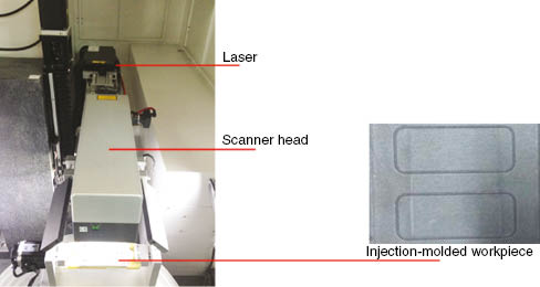
Experimental LDS system.
In order to explore the action of a laser, an orthogonal experiment was designed to activate LDS thermoplastic with different parameters. Laser scanning speed was 2500 mm/s, PRR was from 30 to 120 kHz, power was from 3 to 19 W, and pulse width was from 14 to 200 ns. The injection-molded workpiece in Figure 1 was made from LDS thermoplastic. This thermoplastic material is SABIC® DX11355. It is a polycarbonate (PC)-based compound. The workpiece was activated as a substrate. The activating process is close to laser engraving on the substrate. Figure 2 shows the results. The horizontal coordinate is the PRR. The vertical coordinate is the power of the laser. Every grid was activated by different PRR and laser power.
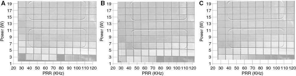
The results were activated by 50 ns (A), 100 ns (B) and 200 ns (C) width of the laser pulse.
The electroless copper plating method is used to plate Cu on thermoplastic. This plating method can be generally described by the following two half-cell reactions:
Anodic reaction
Cathodic reaction
where L represents the chelating agent, such as ethylenediaminetetraacetic acid, triethanolamine, or tartaric acid, and m denotes the charge of the chelating agent.
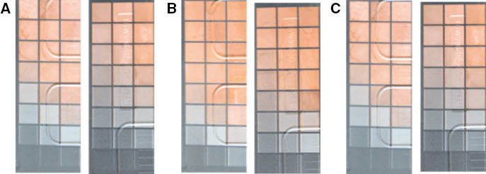
Figure 3 displays results after copper plating. Copper covered areas in the red polygon are qualified plating results. It shows 100 ns laser pulse width is the best parameter for getting widest fabrication. The judgment procedure is presented in the next section.
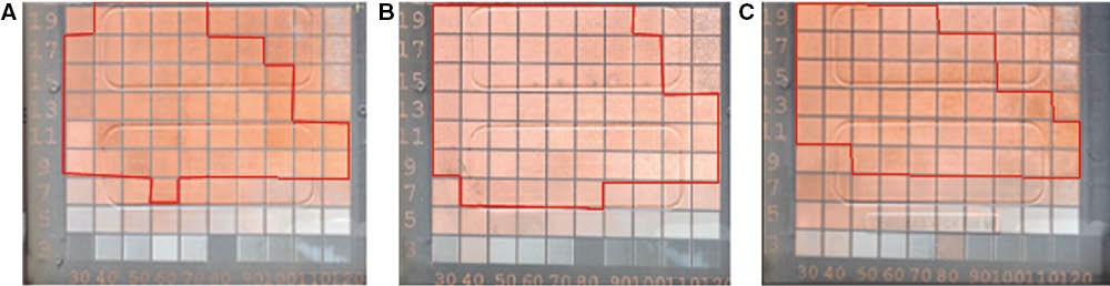
50 ns (A), 100 ns (B) and 200 ns (C) pulse width plating results.
3 Results and discussion
First of all, four evaluation levels were used to estimate the different qualities of plating. A sample plating area was separated into many square sections by knife (square size: 3 mm×3 mm), and then scraped off by scotch tape. Degree of plating coating damage was used to estimate plating quality.
It is difficult to scrape off plated coating.
Plated coating can be scraped off.
Plated coating is rough and incomplete.
No plated coating.
These activated results were investigated with confocal microscopy. It was shown that the plating quality is related to the roughness profile. Table 1 shows how roughness affects plating quality. The increasing arithmetical mean deviation of the roughness profile (Ra) is properly conducive to get better plating quality. But Ra leads to opposite results when it is too high.
Ra of different laser parameters.
| Laser parameters | 5 W, 90 kHz | 7 W, 90 kHz | 11 W, 90 kHz | 11 W, 120 kHz | 19 W, 120 kHz |
|---|---|---|---|---|---|
| Plating quality | 4 | 2 | 2 | 1 | 4 |
| Ra (μm) | 4.328 | 7.122 | 8.165 | 9.224 | 17.446 |
In Table 1, Ra is used to describe the results. Laser scanning style is line by line. The direction of sampling is perpendicular to laser scanning line as shown in Figure 4.
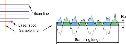
Laser scanning style and sampling method.
An LDS process model was built for further analyzing the activating mechanism in this research. LDS thermoplastic composition comprises various materials. For being convenient to study, based on different melting points between metal and thermoplastic, a simplified model was built. This supposes that there are only two types of particles, thermoplastic particles and metal particles. So the original LDS substrate is described as follows: after the laser beam is focused on thermoplastic particles, part of them are evaporated (Figure 5A). Metal particles are saved because the energy of the laser beam cannot evaporate them (Figure 5B). Metal particles form a metal layer which is the base of plating. Increasing Ra can enhance adhesive force of plated copper. Higher energy results in faster evaporation of thermoplastic particles. Longer pulse width time, higher PRR and power, and slower scanning speed can lead to higher activating energy. But if more energy is converted to heat in a limited area, thermoplastic particles under the metal layer melt and even boil (Figure 5C). So they get a higher Ra, but the metal layer is damaged. This leads to a terrible plating result.
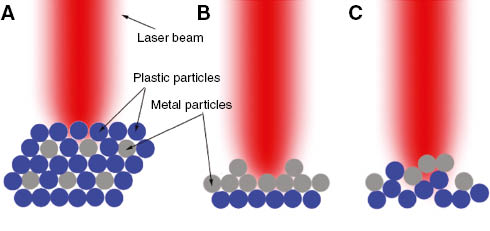
LDS process model.
Figure 6 displays three results of laser activation (100 ns, 2500 mm/s laser scanning speed). They are photography under confocal microscopy: (a) 7 W, 90 kHz; (b) 11 W, 120 kHz and (c) 19 W, 120 kHz. They are further work to confirm the LDS process model as shown in Figure 5. (a) and (b) have a metal layer. But (b) is rougher than (a); (c) is the roughest but its metal layer is damaged.
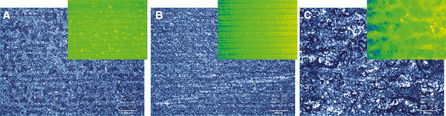
Laser-activated results under confocal microscopy.
The peak power of the laser (Pp) depends on the pulse repetition rate (F), the pulse width (τ) and average power (P). Their relationship is indicated by the following equation:
The laser activation energy (W) work on the substrate is calculated by the following equation:
where P is the average power of the laser, σ is the absorptivity of LDS thermoplastic, F is PRR, τ is the pulse width, V is the laser scanning speed, and T is the total working time. This model ignores the size of the laser spot and laser beam quality. It rarely focuses on how does laser affect the substrate, and it is in line with the experimental results above. Additionally, three assumptions are proposed and confirmed based on this model:
Shorter and larger F will lead to better LDS quality also. F has a larger adjustment range and competes with P. An experiment was performed for this. Pulse widths of 14 ns, 20 ns and 30 ns were applied for more results which are displayed in Figure 7. The damage issue of the metal layer decreases with the decrease of the pulse width.
The value ranges of P, F and τ are much larger than the range of V, so that V less affects process quality. An experiment was used to confirm that, and Figure 7 illustrates this work. The left of (a) is scanned at 2500 mm/s and the right of (A) at 3750 mm/s. Figure 7(B) and (C) show comparisons with different scanning speeds like Figure 7(A) just with different pulse widths. The figure shows that a 150% difference of scanning speed did not lead to an obvious different result.
Laser scanning speed is 2500 mm/s of each left, and right is 3750 mm/s.
Usually, σ is uncertain for different materials. There is little information about σ LDS material with a 1064 nm laser. In general, darker polymer materials have higher σ for a 1064 nm laser. To find out the influence of σ, more LDS substrates were tested to find minimum parameters of advanced process quality for each material. This work is shown in Table 2, which illustrates that activating parameters should be totally different because of different σ.
Plating results activated by 14 ns (A), 20 ns (B) and 30 ns (C) laser pulse width.
Experimental results of different materials.
| Material | Material 1, black color | Material 2, black color | Material 3, yellow color | Material 4, white color |
|---|---|---|---|---|
| Power (W) | 9 | 9 | 11 | 17 |
| PRR (kHz) | 80 | 70 | 80 | 110 |
| Scanning speed (mm/s) | 2500 | 2500 | 2500 | 2500 |
| Pulse width (ns) | 100 | 100 | 100 | 100 |
To make confirmation of the damaged metal layer, the samples were investigated by a scanning electron microscope (SEM) and energy dispersive spectrometer (EDS) for further analysis [22–24]. The first sample is the original substrate (Figure 8A) which is not activated by the laser. The critical materials of the LDS process in thermoplastic composition are Cr and Cu. There are a lot of high light spots in Figure 8. They are high-contrast. It is speculated that they are metals which are able to conduct electricity. Figure 8B shows the sample activated by a low power laser and there are more high light spots. Figure 8C shows the sample activated by proper power of the laser, and Figure 8D the sample activated by excessive power of the laser. According to Figure 8C, it had the most volume of high light spots and got the best plating.
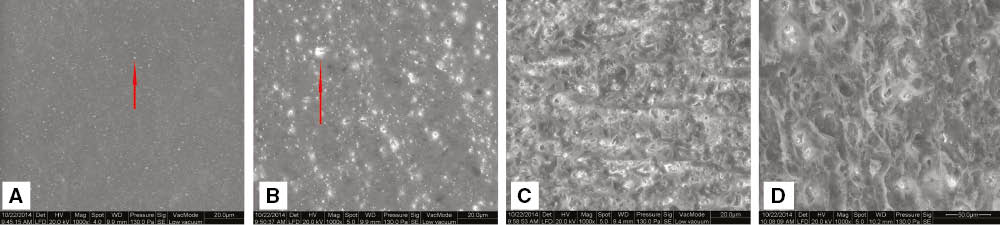
SEM micrographs of activated samples.
Those high light spots on the micrographs were investigated by EDS. Figure 9A shows the EDS result of the high light area on the original sample, and Figure 9B shows the EDS result of the black area. Figure 9A shows higher concentration of Cr and Cu than does Figure 9B.
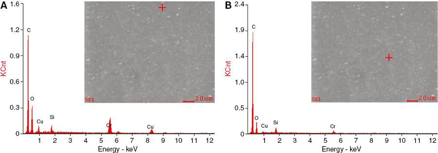
EDS results of original samples.
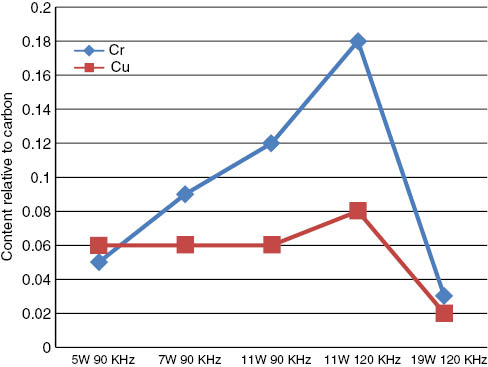
A series of EDS investigations were used to compare the properly activated sample with the excessively activated sample. The contents of Cu and Cr have an obvious relationship with plating quality, and are affected by the LDS process. EDS is limited to measure the absolute content of substances. Nevertheless, LDS thermoplastic comprises a PC polymer in an amount from about 40 wt% to about 70 wt%, a high rubber graft acrylonitrile-butadiene-styrene (HRG-ABS) copolymer in an amount from about 10 wt% to about 25 wt%; and a styrene-acrylonitrile (SAN) copolymer in an amount from about 5 wt% to about 30 wt% [21]. That means the carbon content of LDS thermoplastic is extremely high. Therefore, the materials content relative to the carbon content can be the reference in this research. Figure 10 shows comparison of EDS results. The vertical coordinates mean content relative to carbon. The content of carbon is 1. Plating adheres to Cu and Cr, not carbon. But Cu and Cr are not easy to be quantified. So content relative to carbon was used to quantify Cu and Cr. As the activating laser power increases, the content of Cr and Cu also increases. However, there is still a limitation of the activating laser power. The content of Cr and Cu will be decreased if the power increases and beyond the limitation of the activating laser power.
Comparison of EDS results.
4 Conclusions
This paper presents a model to describe mechanisms during LDS processing, and presents a series of experiments to confirm it. The model and these experiments are valuable for optimizing LDS process.
Meanwhile, a nanosecond pulse laser is successfully applied on LDS. It shows shorter pulse width and higher PRR, which lead to better process quality. This is a direction of parameter selection for LDS processing. This paper also indicates that EDS is a feasible way to investigate thermoplastic and metal with the relative content of metal.
In addition, the laser scanning speed is limited by hardware devices so that value range is smaller compared with pulse width and PRR. In its range, there is less effect on LDS process quality. But the optical absorption of material has greater influence.
This paper shows that about 100 ns laser pulse can get the best processing window. This range of laser pulse width is common in the nanosecond laser, which is a low-cost laser. This is the foundation for large-scale applications. A longer pulse width laser will over-burn thermoplastic to a rough surface. But shorter pulse width from a nanosecond laser does not have enough peak power to activate LDS material. A picosecond laser often has high peak power that is easy to damage all materials. Furthermore, the picosecond laser is also a high-cost solution. So the nanosecond laser is an optimized solution for LDS processing.
Acknowledgments
This work was supported by Beijing Science and Technology committee Project under Grant no. Z140002.
Funding: Beijing Nature and Science Foundation, (Grant/Award Number: ‘Z141100002814011’).
References
[1] Franke J. Three-Dimensional Molded Interconnect Devices (3D-MID), Hanser Gardner Publications: Cincinnati, OH, 2014.10.3139/9781569905524Suche in Google Scholar
[2] Islam A, Hansen HN, Tang PT, Sun J. Int. J. Adv. Manuf. Technol. 2009, 42, 831–841.10.1007/s00170-008-1660-9Suche in Google Scholar
[3] Friedrich A, Geck B, Klemp O, Kellermann H. Microwave Conference (EuMC), Nuremberg, Germany, 2013, 640–643.Suche in Google Scholar
[4] Kaddour D, Tedjini S, Djamel A. APSURSI 2013, 2013, 9, 1502–1503.Suche in Google Scholar
[5] Florence S, Romain P, Frederic G, Daniel G, Francois LP, Christian P. 2013 IEEE AP-S/USNC-URSI, 2013, 7-13, 2217–2218.Suche in Google Scholar
[6] Thomas W. PhD Dissertation, Delft University of Technology, 2014.Suche in Google Scholar
[7] Yang L, Bin L. Eng. Plast. Appl., 2013, 7, 100–104.Suche in Google Scholar
[8] Werner T, Johannes P. ECCE 2011, Arizona, USA. 325–332. Doi: 10.1109/ECCE.2011.6063787.Suche in Google Scholar
[9] Jianhua H, Caiping Z, Lina X. China Light & Lighting, 2015, 1, 29–33.Suche in Google Scholar
[10] Gries D. Laser Focus World 2010, 46, 59.Suche in Google Scholar
[11] Yoon S, Choi K, Baek S, Chang H. Electrical Machines and Systems (ICEMS), Beijing, China, 2011, 1–3.10.1109/ICEMS.2011.6073785Suche in Google Scholar
[12] Bachyl B, Franke J, Packaging, IMPACT 2014, Taipei, China, 437–444. Doi: 10.1109/IMPACT.2014.7048377.10.1109/IMPACT.2014.7048377Suche in Google Scholar
[13] Kordass T, Franke J. ISSE 2014, Dresden, Germany, 491–495. Doi:10.1109/ISSE.2014.6887650.Suche in Google Scholar
[14] Tam S, Lee S, Pong B, Pang D. U.S. Patent 8642387, 2014.Suche in Google Scholar
[15] Paul CY, Rong L. U.S. Patent 20130106659, 2013.Suche in Google Scholar
[16] Schrauwen B, Antonius G. U.S. Patent 20150035720, 2015.Suche in Google Scholar
[17] Yanjun L, Jiru M, David Z. U.S. Patent 8309640, 2012.Suche in Google Scholar
[18] Qiang J, Siguang J, Jiru M, Tong W, Xiangping Z. U.S. Patent 20120276390, 2012.Suche in Google Scholar
[19] Tong W, Yunan C, Yangang Y. U.S. Patent 20140206800, 2014.10.5465/ambpp.2014.14174abstractSuche in Google Scholar
[20] Yunan C, Xiaofeng Y, Yuxian Y. U.S. Patent 20140296410, 2014.Suche in Google Scholar
[21] Jiru M, David Z, Qiang J, U.S. Patent 20140076616, 2014.Suche in Google Scholar
[22] Xiao W, Hao C, Huixia L, Pin L, Zhang Y, Chuang H, Zhenuan Z, Yuxuan G. Opt. Las. Eng. 2013, 51, 1245–1254.10.1016/j.optlaseng.2013.04.021Suche in Google Scholar
[23] Sanjay M, Vinod Y. Opt. Las. Eng. 2013, 51, 681–695.10.1016/j.optlaseng.2013.01.006Suche in Google Scholar
[24] Soni A, Patel RK. Int. J. Eng. Sci. Innovat. Technol. 2013, 2, 389–396.Suche in Google Scholar
©2016 Walter de Gruyter GmbH, Berlin/Boston
Artikel in diesem Heft
- Frontmatter
- Original articles
- Preparation and characterization of graphene oxide/PMMA nanocomposites with amino-terminated vinyl polydimethylsiloxane phase interfaces
- Effect of exfoliated graphite nanoplatelets on thermal and heat deflection properties of kenaf polypropylene hybrid nanocomposites
- Synthesis of spherical porous cross-linked glutaraldehyde/poly(vinyl alcohol) hydrogels
- Influence of process parameters on property of PP/EPDM blends prepared by a novel vane extruder
- Influence of processing conditions on heat sealing behavior and resultant heat seal strength for peelable heat sealing of multilayered polyethylene films
- Thermal degradation kinetics and lifetime of HDPE/PLLA/pro-oxidant blends
- Effect of notch sensitivity on the mechanical properties of HA/PEEK functional gradient biocomposites
- The influence of melt mixing on the stability of cellulose acetate and its carbon nanotube composites
- Experimental analysis of resin infusion in air cushion method
- 3D-MID manufacturing via laser direct structuring with nanosecond laser pulses