Optimization of non-linear conductance modulation based on metal oxide memristors
-
Huan Liu
Huan Liu is studying for a Master’s degree at the University of Electronic Science and Technology of China. She is doing research on the thin-film memristor, especially its optimization.
Min Wei received her PhD in 2012 from the University of Electronic Science and Technology of China. She was a visiting scholar in the University of California Santa Cruz from 2013 to 2014. Now, she is an Associate Professor in the University of Electronic Science and Technology of China. She is doing research on thin films and integrated devices.
 and
Yuzhong Chen
and
Yuzhong Chen
Yuzhong Chen is studying for a Master’s degree in the University of Electronic Science and Technology of China. He is doing research on thin-film devices.

Abstract
As memristor-simulating synaptic devices have become available in recent years, the optimization on non-linearity degree (NL, related to adjacent conductance values) is unignorable in the promotion of the learning accuracy of systems. Importantly, based on the theoretical support of the Mott theory and the three partial differential equations, and the model of conductive filaments (CFs), we analyzed and summarized the optimization schemes on the physical structure and the extra stimulus signal from the internal factor and external influence, two aspects, respectively. It is worth noting that we divided the extra stimulus signals into two categories, the combined pulse signal and the feedback pulse signal. The former has an internal logical optimized phenomenon, and the composition of only two parts in each cycle leads to a simple peripheral circuit. The latter can obtain an almost linear NL curve in software stimulation because of its feature in real-time adjustment of signals, but it is complex in hardware implementation. In consideration of space and energy consumption, achieving memristor with different resistive switching (RS) layers can be another optimization scheme. Special attention should be paid to the weaker NL, which could improve learning accuracy at the system level only when the value of other non-ideal properties such as the on/off ratio is within a certain range.
1 Introduction
The memristor is widely viewed as a potential device in neuromorphic systems as its analog resistive switching (RS) process is suitable to simulate the weight update of a biological synapse (bio-synapse), after showing its developing advantage in recognizing the digital state of storage [1], [2], [3], [4] and analog states of computational fields [5], [6], [7], [8], [9], [10]. Nearly a decade of research has reinforced the realizability of memristors in this application area. In these neural morphic applications, the memristor needs to exhibit an analog RS behavior (having multi-resistance states) rather than binary resistance states, and some of its non-ideal properties lead to a negative influence on the learning accuracy of the neuromorphic system [11], [12], [13]. The focus of this review is on the performance optimization of a memristor, and the optimization object is the non-ideal characteristic of the conductance modulation of the memristor. The key sections of the review are Sections 2 and 3, which discuss the theory and mechanism of supporting the optimization object and the feasible schemes from the external conditions to achieve optimization, respectively.
To make a clear comparison between the memristor and the bio-synapse, a model diagram of these two concepts is shown in Figure 1. The weight update of the bio-synapse is the basis for transmitting and processing information [14], [15], [16], and the continuous conductivity state switching of memristors can mimic this function of a bio-synapse by enabling the distribution of multiple conductance states [17], [18], [19], [20], [21]. So a common concept, non-linearity (NL for short) of the state distribution, becomes the key point. Within this article, all of the non-linear terms we are talking about refer to NL in conductance modulation of a memristor, also known as the NL in the weight update of a synaptic device. A memristor with an ideal NL (=0) can simplify the weight update process and hardware circuit, and improve the learning accuracy [22] in a neuromorphic system. The most intuitive expression of the device with a higher NL (close to 1) is the phenomenon of two stages in conductance modulation curves [23], [24], [25], [26], [27], [28], and a detailed explanation of NL is given in the second part of this article.
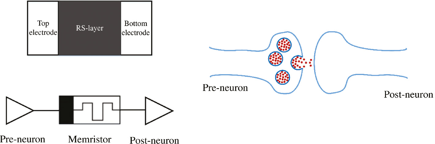
Comparison between the bio-synapses and the artificial synapses (memristors).
Metal oxide memristors usually have a typical metal-insulator-metal (MIM) structure, and its insulator layer (also known as the RS layer) is made by binary metal oxides (e.g. TiO2 [28], [29], [30], [31], WOx[32], [33], TaOx [34], [35], [36], [37], [38], [39], [40], [41], [42], HfO2 [43], [44], [45], [46], [47], etc.), perovskite metal oxides [48], [49], chalcogenes [50], [51], and others. Although the RS mechanism of a memristor does not have a unified conclusion so far, the conductive filament (CF) model based on ion/vacancies migration in many research conclusions can give a good degree of coverage of the corresponding experimental data. For example, Shigeoka et al. [52] showed the work on a memristor based on Ta2O5 by using the CF model. Bousoulas et al. [53] demonstrated its research on Ti/TiO2−x-based memory devices based on the CF mechanism. Qu et al. [33] demonstrated the reason for the existence of CFs using the experimental results of a WOx-based memristor. In addition, migration of ions/vacancies in the RS layer is thought to be associated with NL [5], [37], [38], [39], 54], [55], and further calculations of particle migration provide theoretical support using the Mott theory and the finite element method (FEM) [56], [57], [58]. The Mott theory was the cornerstone of research related to particle migration. The FEM uses the mathematical method to simulate the real physical system and is used as the model basis for the internal state analysis of memristors. Kim et al. [59], [60], [61], [62], [63] used this model in a series of research related to memristors in recent years. Based on these theories, scientists focused much of their attention on the optimization scheme of NL based on the ion transport of an RS material, such as doping and the multi RS layer [64], [65].
For other optimization schemes of NL, using smarter stimulus signals are suggested, which looks for a series of signals that balances the device between NL and feasibility. In this review, Section 2 is about NL optimization in a simple one-dimensional (1D) rigid point ion model proposed by Mott and Gurney [66], which results in a self-consistent solution of three partial differential equations (PDEs). Two kinds of NL optimization schemes, the smarter stimulus signal and the multi RS layer, are stated in Sections 3 and 4, respectively. In Section 5, we summarize the optimization schemes, from the four aspects of NL optimization, feasibility, novelty degree, and consumption. In Section 6, we summarize the direct and indirect effects of NL change on learning accuracy in a neuromorphic system.
2 Causes of the two-stage phenomenon
2.1 The two-stage phenomenon
The I-V curve cluster is the most common form of graphic used in characterizing a multi-state modulation of a memristor, which is taken by applying voltage sweeps with a certain value of the termination voltage (Vstop) or a certain value of the complaint current (Icc). The I-V curves are the basic characterization method in the field of memristor research. At the same time, in order to study the analog RS behavior of the memristor, especially its linearity of the conductance modulation, the characteristic curve that indicates the conductance to change with the increase in the external stimulus loading time becomes the main means, as shown in Figure 2.
![Figure 2: Multi-level RS behavior and the two-stage phenomenon in conductance modulation in the memristor. (A) Mult-ilevel resistive switching properties of the Pd/WO3/W device obtained by applying DC sweeps. The number in this figure indicates the sweep sequence. Blue, the set process; red, the reset process. Adapted with permission from Ref. [25]. Copyright 2011 Applied Physics A Materials Science and Processing. (B) Non-linear conductance modulation curve with ideal symmetric P/D curves and normalized conductance as the Y-axis. (C) Ta/TaOx/TiO2/Ti device. Non-linear conductance modulation curve obtained by applying AC pulses successively. The hollow point is experimental data, and the black solid curve is the simulation results. Adapted with permission from Ref. [67]. Copyright 2015 Scientific Reports.](/document/doi/10.1515/ntrev-2018-0045/asset/graphic/j_ntrev-2018-0045_fig_002.jpg)
Multi-level RS behavior and the two-stage phenomenon in conductance modulation in the memristor. (A) Mult-ilevel resistive switching properties of the Pd/WO3/W device obtained by applying DC sweeps. The number in this figure indicates the sweep sequence. Blue, the set process; red, the reset process. Adapted with permission from Ref. [25]. Copyright 2011 Applied Physics A Materials Science and Processing. (B) Non-linear conductance modulation curve with ideal symmetric P/D curves and normalized conductance as the Y-axis. (C) Ta/TaOx/TiO2/Ti device. Non-linear conductance modulation curve obtained by applying AC pulses successively. The hollow point is experimental data, and the black solid curve is the simulation results. Adapted with permission from Ref. [67]. Copyright 2015 Scientific Reports.
Figure 2A shows the corresponding experimental results of the I-V relationship based on the TE/HfOx/AlOx/BE memristor device, by Kim et al. [59]. In order to obtain more intuitive expression of conductance distribution, the conductance-cycle number (or time) curves are necessary. A high-degree fitting results of the experiment is introduced here to prove the phenomenon of segmentation (Figure 2C), by Wang et al. [67], by applying a pulse sequence with a constant value in amplitude and frequency (called identical pulse), based on the Ta/TaOx/TiO2/Ti memristor.
Figure 3 lists several conductance modulation curves for a memristor with different materials or structures. Not only is this found in the usual two-terminal memristor, a similar phenomenon also occurs in the three-terminal memory transistors [61], [63], [71], [72], [73], [74], [75], [76], [77], [78]. Zhu et al., from Beijing University, developed the WSe2-based synaptic transistors. This device shows good performance, especially in terms of conductivity modulation linearity and low energy consumption [61]. In this work, there are no obvious two-stage phenomena in the conductance modulation curve, and the ultralow energy consumption of ≈30 fJ per spike is achieved. The conductance modulation curves show different forms, especially in the aspect of the slope. Based on these results, it can be concluded that the slope of the curve shows a segmentation phenomenon. The segmentation of the slope of the curve in conductance modulation curves of a memristor device is not a special case, but occurs in the vast majority of experiments. Das et al. [79] found the segmentation phenomenon at the Y2O3-based memristor. Banerjee et al. [80] found this phenomenon for the TiOx/Al2O3-based memristor. Guangyang et al. [72] found this phenomenon at the SnO2-based memristor. The segmentation phenomenon is described as a two-stage phenomenon here in the aspect of the metal oxide memristor.
![Figure 3: Non-linear conductance modulation curves. (A) Pt/HfOx/ZnOx/TiN memristor device. Adapted with permission from Ref. [68]. Copyright 2017 Nanoscale Research Letters. (B) TiN/TaOx/Pt memristor device. Adapted with permission from Ref. [69]. Copyright 2016 Nanoscale. (C) Pt/TiN/PCMO/Pt memristor device. Adapted with permission from Ref. [26]. Copyright 2010 Nano Letters. (D) Ta/ethyl viologen diperchlorate [EV(ClO4)2]/triphenylamine-based polyimide (TPA-PI)/Pt memristor device. Adapted with permission from Ref. [70]. Copyright 2016 Journal of Materials Chemistry C.](/document/doi/10.1515/ntrev-2018-0045/asset/graphic/j_ntrev-2018-0045_fig_003.jpg)
Non-linear conductance modulation curves. (A) Pt/HfOx/ZnOx/TiN memristor device. Adapted with permission from Ref. [68]. Copyright 2017 Nanoscale Research Letters. (B) TiN/TaOx/Pt memristor device. Adapted with permission from Ref. [69]. Copyright 2016 Nanoscale. (C) Pt/TiN/PCMO/Pt memristor device. Adapted with permission from Ref. [26]. Copyright 2010 Nano Letters. (D) Ta/ethyl viologen diperchlorate [EV(ClO4)2]/triphenylamine-based polyimide (TPA-PI)/Pt memristor device. Adapted with permission from Ref. [70]. Copyright 2016 Journal of Materials Chemistry C.
For a two-stage phenomenon, the slope of the curve is usually segmented to a clear two stages, as the initial stage is significantly higher than the tail, as shown in Figure 2C. In detail, the abrupt change in the adjacent conductance value(∆G) occurs in the first stage, and the gentle change reaches the saturation conductance value (Gmax) in the second stage. Either memristors exhibit a continuous increase or a continuous decrease in conductance value upon a stimulation pulse with an opposite polarity, corresponding to the characteristics of bio-synapses, and these two behaviors can be called long-term potentiation (LTP) and long-term depression (LTD), respectively [81], [82], [83], [84]. In order for this phenomenon to be effectively analyzed, the concept of NL proposed by Wang et al. in 2016 [85] was adopted.
Eq. (1): GLTP(n) and GLTD(n) are the conductance values after the nth LTP-pulse and LTD-pulse, respectively. N is the number of LTP-pulse/LTD-pulse.
This concept is based on the image representation shown in Figure 2B, in which the LTP and LTD are symmetrically characterized in one dialog, for facilitating the conformance of NL, and NL is defined as Eq. (1).
2.2 Theoretical basis
As a key research direction of memristors in the aspect of internal mechanism, particle migration has been continuously appearing in related research papers. This foundation provides theoretical support for other optimization work. Kim et al. [57], [59], Prezioso et al. [29], [86], [87], [88], and Matveyev et al. [10], [89], [90], [91] used this as a support to propose NL optimization. Sung et al. [92] worked on optimization on the I-V linearity. Garbin et al. [93] worked on optimization on variability. It is worth mentioning that Mott first proposed the theory of particle migration in 1948 [94], called the Mott theory, shown as Eqs. (2) and (3), to describe particle migration. Here, a is the effective escape distances, and Ea is the activation energy for the hopping process, and they are all determined by the kind of particle and the kind of material in which the particles migrate.
Eqs. (2) and (3): D is the ion diffusivity, f is the attempt-to-escape frequency, Ea is the activation energy for the hopping process, a is the effective hopping distance, T is the local temperature, E is the local electric field, v is the drift velocity, k is the Boltzmann constant, and q is the charge quantity.
Larentis et al. [95] used three partial differential equations to establish a physical model of a memristor driven by particle migration in their paper in 2012. In recent research, this method was followed and optimized by other researchers. In 2014, Kim et al. [60] proved this method by comparing the experimental data from a TaOx-based memristor. After that, they divided the internal state variables w (used to describe the size-doped area) into g (length of CFs) and r (radius of CFs) because of the appearance of the CFs model. This work led researchers to analyze memristors using second-order or even higher-order models. Dipesh et al. [96] made the numerical modeling as the theoretical basis of heat transfer. Sadi et al. [97] made this theory the simulation methodology in their work based on SiOx. For exploring the resistive switching mechanism of a memristor, it is necessary to investigate the activity track and law of carriers in the memristor device bulk. Thus, the simulation of the RS process requires the PDEs: (1) a drift/diffusion continuity equation for VO transport, (2) a current continuity equation for electrical conduction, and (3) a Fourier equation for Joule heating, as shown in Eqs. (4–6).
Vo transport
Current continuity
Joule heating
Eqs. (4–6): nD is the concentration of VO, ψ is the potential, and T is the temperature.
A simulation of this theory can be achieved through the establishment of an effective model based on the finite element method (FEM), in which the value of nD, ψ, and T can be calculated within a numerical solver. The establishment of the model requires a one-to-one correspondence with the structure of the memristor. In particular, the multi-layer RS layers of different materials cannot be mixed together for discussion. In order to facilitate the explanation of this theory, the CF model of a memristor with a simple structure based on FEM is given here (Figure 4A, B). All of the meanings and units of the variables or constants, involved in the Mott theory and the three PDEs, are summarized in Table 1.
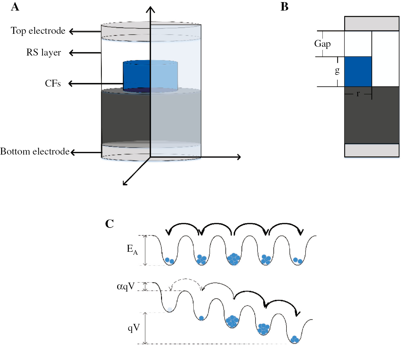
Model of memristor based on the FEM and the particle transition model. (A) 3D CF model of a memristor with a simple structure based on FEM. (B) 2D CF model of a memristor. (C) Particle transition model.
The detailed information of the three PDE-related parameters.
| Char. | Unit | Meaning |
|---|---|---|
| Parameters in constants | ||
| a | Nm | Hopping distance |
| Ea | eV | Ion migration energy barrier |
| f | Hz | Escape attempt frequency |
| γ | – | γ=1 for DC |
| γ=2 for AC | ||
| Parameters from measurements and assumption | ||
| g | Nm | Length of the CF |
| r | Nm | Radius of the CF |
| rm | nm | |
| ρ | S/cm | Resistivity of the CF |
| σ | Ω−1 cm−1 | Electrical conductivity |
| σ0 | Ω−1 cm−1 | Electrical conductivity pre-exponential factor |
| EAC | eV | Activation energy for conduction |
| Dependent variables | ||
| nD | cm−3 | Concentration of VO |
| T | K | Temperature |
| ψ | V | Potential |
| Parameters about particle migration | ||
| v | cm s−1 | Drift velocity |
| D | cm2 s−1 | Diffusivity |
| S | K−1 | Soret diffusion coefficient |
| Flux | ||
| D∇nD | Fick diffusion flux | |
| V nD | Fick drift flux | |
| D S nD∇T | Soret diffusion flux | |
| Parameters for current | ||
| I0 | A | – |
| V0 | V | |
| gm | nm | |
| Parameters determined by materials | ||
| μ | kg/cm3 | Ion mobility |
| Cp | J K−1 cm−3 | Heat capacitance |
| kth | W cm−1 k−1 | Thermal conductance |
| δ | – | Heat dissipation factor |
| H | – | Temporal heat factor |
Ion migration is described by a flux in units (cm−2 s−1), including diffusion (jdiff) and drift (jdrift) [57], [95] components, as the Mott theory elaborates. Both these two processes rely on ion hopping. External electric field stimulation will change the difficulty of particle migration. Specifically, in the direction of the electric field, the barrier of particle migration decreases, and particles migrate easier toward the same direction. On the contrary, particle migration becomes more difficult in the opposite direction of the external electric field. This process results in a directional ion drift (Figure 4C). On the other hand, the diffusion process of ions depends on both the temperature gradient and the carrier concentration gradient. Therefore, calculating the carrier concentration distribution in the device bulk is of great significance for investigating the RS mechanism of it.
To solve the three PDEs, boundary conditions of ψ and an approximately maximum carrier density are needed, as shown in Table 1. A model for electrical conductivity in the RS layer and in CFs is considered to be thermally activated, as shown in Table 1.When making calculations, the researchers assume that σ0, EAC, and kth are linearly related to nD, and the relevant starting and ending values are related to the material of the RS layer. It must be said that such assumptions have been verified [56], [58], [95] as not affecting the validity of the calculations. In the early simulations, the factor of temperature in the memristor device bulk was generally ignored. The specific operation was to set the device bulk temperature equal to room temperature (T0), and regard the heat transfer or divergence. It has been verified [57], [98] that such assumptions lead to large differences between the calculated and experimental results. The Joule heating [62], [99], [100], [101], [102], caused by CF connectivity in the device, causes a significant temperature change in the device when it is in the RS process, affecting particle diffusion process, so as for the conductivity of the device.
2.3 Particle migration in two stages
From the perspective of the CF morphological changes in the memristor alone, conclusions that are consistent with the three PDEs simulation results can be obtained. Alessandro et al. [103] used the CF model to be the explanation of their experimental results. Lu et al. [104] made their research based on the CF model and showed the two-stage phenomena in the forming process of the CFs. Zhu et al. [65] used simulated 2D maps to indicate the oxygen vacancy (VO) concentration distributions in a memristor, in which there is significant expanded phenomena in the horizontal direction about the CFs. In order to more intuitively demonstrate the impact of particle migration on the RS behavior, we summarized and made a diagram of it shown in Figure 5. VOs are present as doping in PDE simulation and are considered as constituent substances of the CFs. Similarly, the continuation of the conclusion by Gao et al. [24], [105] in this subsection places the VOs as the main object. It acts as a carrier in the memristor device bulk, and there is migration within the device so that the device can complete the RS process.
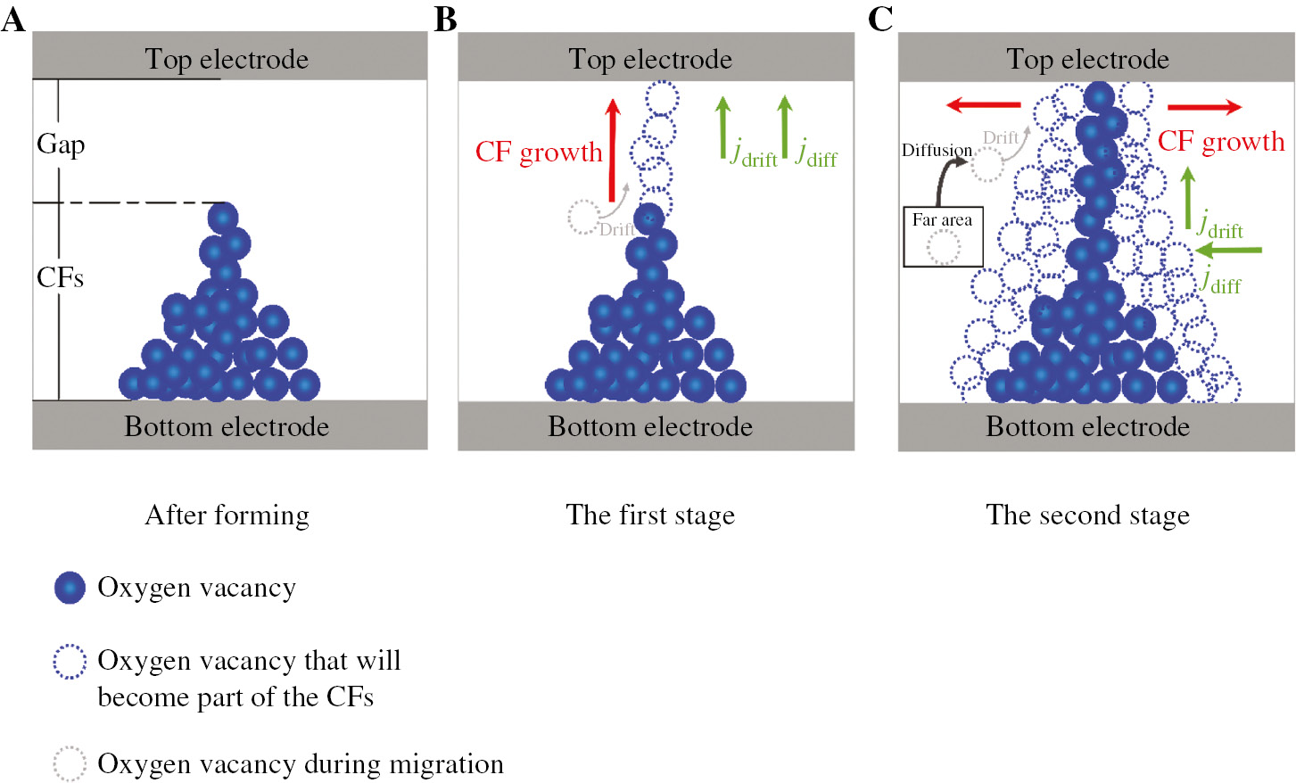
Vo migration model in a two-stage process in conductance modulation of a memristor. (A) Initial state of the memristor based on the CF model. (B) Model of processes that dominate VO migration in the first stage. (C) Model of processes that dominate VO migration in the second stage.
The reason for the two-stage phenomenon discussed in this review is analyzed with the features of the conductance modulation curves. The model shown in Figure 5 shows the direction of the CF growth in the memristor device and the effects of the migration of the VOs in different stages of stimulation. The memristor is initially in an off state, which means a high resistance state (HRS), and there are no CFs in the body. Forming process promotes the formation of CFs by applying external stimuli in the form of voltage that is slightly higher than the RS voltage. At the end of this process, which is to remove the voltage stimulus, there are incomplete CFs formed in the memristor device. At this moment, the device is in the HRS state, and a gap [106], [107], [108], [109] exists inside it. By applying external stimuli to the device, the gap will be filled with VOs, and the CFs grow to connect the cathode and anode eventually, which is called the set process. At this moment, the device is in the low-resistance state (LRS). Conversely, when voltage stimulus with opposite polarity is provided in the on state, the VOs migrate in the opposite direction. The CFs break after this processing, and the device returns to the off state with incomplete CFs, which is called the reset process.
In the set process, the morphological changes of CFs have different trends with the increase in stimulus loading time. The memristor device is in the first stage at the beginning, when the identical pulse is applied to it. Before the CFs are complete, there is a high electric field in the gap area, and the VO (or ion) transmission will be controlled by the drift process, which is driven by an electric field effect, along the VO concentration gradient. The main change in the CFs is their length [110], as shown in Figure 5B, which leads to rapid increase in the conductance of the device so that the conductance modulation curve shows a higher slope and the conductance state distribution is sparse. Another important feature in the first stage is that although the conductance value of the memristor can achieve a substantial increase within a smaller number of pulses, it is unsaturated. The reason is that Vos in the area near the CFs step into the reduction reaction in the first stage [60], and VOs in the area farther away from the CFs need to migrate for a long distance before it, which happens in the second stage. In the first stage, there is just part of the VOs that can participate in the formation of the CFs, and the CFs are not strong enough. When the curve steps into the second stage, the CFs become complete, and the device tends to be metalized. The complete CFs resulted in the reduction of the local electric field, which results in the suppression of the drift process, through the Mott theory shown in Eqs. (2) and (3).
In the second stage, there are obvious differences in the internal changes of the device from the first stage, which must be paid attention to. Several studies simulated the temperature changes inside the device during the RS process and obtained the temperature distribution results with a consistent trend – the areas near the CFs have a higher temperature. Kim et al., from the University of Michigan, worked in this area [56]. Larentis et al., from the University of Texas, did relevant work [95]. Jeong et al. did this work in 2015, and here, we quote their work as shown in Figure 6[104]. The Joule heating caused by the connected CFs results in a significant temperature gradient that leads to an increased local temperature, as shown in Figure 6. Therefore, the particle diffusion process was enhanced in the second stage, so the CFs can expand in the horizontal direction. Especially, this partial migration process is dominated by the temperature gradient rather than the concentration gradient. In detail, the local temperature of the area where the CFs are located is higher than those of the other areas, which leads to particles migrating toward the CFs. This process can be named as the thermophoresis process as a result of the temperature gradient. The diffusion of the VOs promotes the expansion of the CFs in the horizontal direction [56], [72], [98], [111], which leads to stronger CFs. The reason for the saturated state in this stage is that the VOs inside the device bulk that can reach the area where the CFs are located are gradually depleted. Therefore, at the end of the set process, conductance is saturated, and there is no more significant increase when the VOs in the area, even if far away from the CFs, is exhausted.
![Figure 6: Simulated temperature distribution in the Pd/Ta2O(5−x)/TaOy/Pd device at different points. Reprinted with permission from Ref. [104]. Copyright 2015 Applied Physics Letters. (A) Point during the first stage. (B) Point during the first stage.](/document/doi/10.1515/ntrev-2018-0045/asset/graphic/j_ntrev-2018-0045_fig_006.jpg)
Simulated temperature distribution in the Pd/Ta2O(5−x)/TaOy/Pd device at different points. Reprinted with permission from Ref. [104]. Copyright 2015 Applied Physics Letters. (A) Point during the first stage. (B) Point during the first stage.
3 The smarter stimulus signal
Spikes were the first to be chosen as a signal source in the memristor stimulus that exists to mimic the type of stimulus signal that a bio-synapse accepts [87], [100], [112], [113]. The device can exhibit LTP and LTD features similar to bio-synapses under continuous spiking stimulation. In addition, stimulated by paired spikes, the memristor device can also achieve the paired-pulse facilitation (PPF) [72], that is, the paired signal is processed by the device to show that the state of the second signal amplitude is greater than the first one. In recent years, in order to simplify the peripheral signal generator circuit, the rectangular pulse signal source is used in the simulation of research about the analog memristor device [114], [115], [116], [117], [118]. The amplitude of the pulse signal determines whether the device can achieve RS or not and the value of ∆G in the RS process. The frequency of the pulse signal determines whether the conductance value caused by the previous pulse can be maintained until the next pulse arrives at the device.
3.1 Identical pulse
In the simplest form, a pulse sequence with a constant amplitude and frequency, here called the identical pulse, is used as a signal source for stimulating the device (Figure 7A), which is also the signal form commonly used in research in recent years. Stimulated by this signal source, the device generally shows segmented phenomenon in the distribution of conductance value. We collected research data related to an analog RS behavior in the field of memristors in recent years and summarized the experimental results based on the identical pulse, as shown in Table 2. The data in the table shows that the material composition of the memristor and the amplitude and the width of the identical pulse signal all have an effect on the experimental data. Based on the data in Table 2, we determine the factors that influence the optimization of NL in the composition of the external stimulus signal and the material composition of the memristor.
![Figure 7: Identical pulse and the response of the memristor to the pulse. (A) Identical pulse. (B) Conductance modulation curves of the programming pulse with different amplitudes based on the Pd/Ta2O(5−x)/TaOy/Pd memristor device. Adapted with permission from Ref. [104]. Copyright 2015 Applied Physics Letters. (C) Multiple memory model. (D) Conductance modulation curves of the programming pulse with different amplitudes and tpp based on the Ta2O(5−x)-based memristor device. Adapted with permission from Ref. [98]. Copyright 2015 Nano letters.](/document/doi/10.1515/ntrev-2018-0045/asset/graphic/j_ntrev-2018-0045_fig_007.jpg)
Identical pulse and the response of the memristor to the pulse. (A) Identical pulse. (B) Conductance modulation curves of the programming pulse with different amplitudes based on the Pd/Ta2O(5−x)/TaOy/Pd memristor device. Adapted with permission from Ref. [104]. Copyright 2015 Applied Physics Letters. (C) Multiple memory model. (D) Conductance modulation curves of the programming pulse with different amplitudes and tpp based on the Ta2O(5−x)-based memristor device. Adapted with permission from Ref. [98]. Copyright 2015 Nano letters.
Summary of response of conductivity distribution to identical pulse scheme in memristor devices.
| Materials | Programming pulse | Nc (#) | ∆Gtotal | Ref. | Year | ||||
|---|---|---|---|---|---|---|---|---|---|
| RS layer | TE | BE | A (V) | Width | N (#) | ||||
| Ta2O5−x/TaOy | Pd | Pd | −0.9 | 100 μs | 150 | ≤25 | ~0.2 mS | [60] | 2014 |
| 1.1 | 10 μs | – | ~0.2 mS | ||||||
| Si2.7%: Ta2O5−x/TaOy | −0.9 | 100 μs | ≤25 | ~0.3 mS | |||||
| 1.1 | 10 μs | – | ~0.7 mS | ||||||
| Si4.2%: Ta2O5−x/TaOy | −0.9 | 100 μs | ≤25 | ~0.5 mS | |||||
| 1.1 | 10 μs | – | ~0.5 mS | ||||||
| Ta2O5−x/TaOy | Pd | Pd | −1 | 100 ns | 20 | ≤5 | ~1.5 mS | [90] | 2015 |
| −0.9 | ~1 mS | ||||||||
| −1.3 | ~2.5 mS | ||||||||
| TaOx/TiO2 | Ta | Ti | 8.7 | 50 μs | 20 | ≤10 | ~90 nS | [67] | 2015 |
| −7 | ~130 nS | ||||||||
| −10 | ~120 nS | ||||||||
| 9.5 | ~130 nS | ||||||||
| 9.2 | ~120 nS | ||||||||
| −8 | ~130 nS | ||||||||
| TaOx/TiO2 | Ta | Ti | 3 | 5 ms | 70 | ≤10 | ~60 nS | [86] | 2016 |
| 3 | 50 | ~50 nS | |||||||
| −3 | 50 | ~50 nS | |||||||
| Ta2O5−x/TaOy | Pt | Pt | 0.9 | 5 μs | 100 | ≤25 | ~0.4 mS | [65] | 2017 |
| TiO2:Ag | Ag | Pt | 0.4 | 200 ns | 30 | ≤20 | ~0.8 mS | [119] | 2018 |
| 300 ns | ≤16 | ~1.8 mS | |||||||
| 500 ns | ≤8 | ~3.8 mS | |||||||
| 0.6 | 200 ns | ≤15 | ~3.9 mS | ||||||
| 0.8 | ≤5 | ~4.0 mS | |||||||
| HfO2 | TiN | TiN | 1.5 | 10 μs | 300 | ≤25 | ~0.4 mS | [89] | 2015 |
| 1.2 | ≤50 | ~0.15 mS | |||||||
| −2 | ≤25 | ~0.85 mS | |||||||
| HfO2 | TiN | TiN | 0.85 | 1.5 μs | 150 | – | 0 | [90] | 2015 |
| 1 | ≤25 | ~20 μS | |||||||
| 1.2 | ≤10 | ~90 μS | |||||||
| −1.2 | – | 0 | |||||||
| −1.6 | ≤50 | ~80 μS | |||||||
| HfO2 | Ti/TiN | TiN | 0.8 | 100 ms | 100 | ≤10 | ~200 μS | [120] | 2016 |
| 0.8 | 1 μs | ≤10 | ~50 μS | ||||||
| −1 | 1 μs | – | ~50 μS | ||||||
| −1.1 | 1 μs | ≤50 | ~150 μS | ||||||
| 0.9 | 10 ms | 60 | ≤20 | ~50 μS | |||||
| 10 μs | ≤10 | ~20 μS | |||||||
| HfOx/HfO2 | Ti | TiN | 0.8 | 100 ms | 100 | ≤10 | ~200 μS | [121] | 2016 |
| −1.1 | 1 μs | ≤25 | ~175 μS | ||||||
| −1 | 1 μs | – | ~50 μS | ||||||
| HfOx/ZnOx | Pt | TiN | −0.2 | 100 ms | 125 | ↑ | ~0.4 mS | [68] | 2017 |
| 1 | 100 ms | ↓ | ~0.6 mS | ||||||
| Nb2O5 | Al | Al | 1.5 | 10 μs | 100 | ≤10 | ~90 mS | [122] | 2014 |
| WOx | W | Pd | 3 | 400 μs | 50 | ≤10 | ~20 μS | [123] | 2014 |
| ZnO | Ti | Pt | 5 | 180 ms | 60 | ↑ | ~5 mS | [124] | 2016 |
| TiOx | Pt | TiN | 3 | 1 ms | 100 | ≤40 | ~600 nS | [125] | 2016 |
| 2.5 | – | ~200 nS | |||||||
| −3 | ≤20 | ~600 nS | |||||||
| −2.5 | ≤40 | ~400 nS | |||||||
| FeOx | Pt | Pt | 1.6 | 100 μs | 50 | ≤10 | ~0.4 mS | [126] | 2016 |
| 10 μs | ≤5 | ~0.3 mS | |||||||
| 1μs | ≤10 | ~0.2 mS | |||||||
| 1.5 | 10 μs | 50 | ≤10 | ~0.2 mS | |||||
| 1.45 | ≤20 | ~0.1 mS | |||||||
| 1.3 | – | 0 | |||||||
| Y2O3 | Al | n-Si | 2 | 50 ms | 100 | ≤10 | ~10 μS | [79] | 2018 |
| 2 | 100 ms | ≤10 | ~15 μS | ||||||
| 2.5 | 100 ms | ≤40 | ~830 μS | ||||||
| PEDOT:PSS | Ag | Ta | 2 | 50 ms | 50 | ↑ | ~600 mS | [127] | 2013 |
| PCMO | Al | … | 1 | 1 ms | 100 | ≤10 | ~9 nS | [22] | 2013 |
| 2 | ~5 nS | ||||||||
| −2.5 | ~0.4 nS | ||||||||
| −4 | ~100 nS | ||||||||
| PCMO | Pt/TiN | Pt | 3 | 1 ms | 100 | ≤25 | ~80 nS | [128] | 2014 |
| 100 ms | ≤25 | ~100 nS | |||||||
| −3 | 1 ms | ≤25 | ~120 nS | ||||||
| 100 ms | ≤25 | ~1 mS | |||||||
| EV(ClO4)2+PEO/TPy-Fe | Ta | ITO | 3 | 10 ms | 50 | ↑ | ~1.5 nS | [129] | 2016 |
| −2 | ↓ | ~0.75 nS | |||||||
| EV(ClO4)2/TPA-PI | Ta | Pt | 0.5 | 10 ms | 90 | ↑ | ~6 mS | [70] | 2016 |
| −0.5 | ↓ | ~6 mS | |||||||
| AgInSbTe | Ta | Ag | 0.6 | 5 μs | 50 | ≤10 | ~8 mS | [130] | 2017 |
| −0.6 | ≤10 | ~8 mS | |||||||
| Lignin | Au | ITO | 0.7 | 100 ms | 50 | ≤20 | ~30 μS | [131] | 2017 |
| −0.7 | ≤20 | ~30 μS | |||||||
–, there is no obvious two-stage phenomenon; ↑↓, apparent linearity; A, the pulse amplitude; N, the total number of the programming pulse; Nc, the pulse number at the critical point; ∆Gtotal, the difference between the maximum conductance and the minimum conductance.
An obvious conclusion can be drawn from Table 2 that most binary metal oxide-based memristors have a two-stage phenomenon of conductance modulation. From the aspect of the stimulus signal, the intensity of the two-segment phenomenon is closely related to the amplitude and width of the stimulus signal.
The amplitude of the identical pulse signal is the value of the extra voltage applied on the device or the electric field that forces the particle migration inside the device. According to the Mott theory in the second part of this review, the applied electric field is the main influence factor of the process of particle drift [104], [110], which is enough to affect the formation rate of CFs at the beginning of a complete CF formation. A simple change in this eigenvalue of the identical pulse signal (from one constant to another) was verified to change the state distribution of the memristor device. This change manifests itself as an increase in Gmax and a steeper conductivity modulation curve [22], [104] (Figure 7B). In detail, the blue curve with the lowest pulse amplitude in this graph shows the lowest NL and Gmax, and the red curve with highest pulse amplitude in this graph shows the highest NL and Gmax. For features of the red, the reason is that the increased electric field, caused by the increase in the pulse amplitude, promotes particle drift, so as to increase the number of VOs forming the CFs in the initial state. The conductance value increases because of that, which results in an increase in NL. In short, it is useless to optimize the NL by changing the amplitude of the identical pulse signal. The timing characteristics of the stimulus signal include the duration (called the pulse width (twidth) in the pulse signal) and time interval (tinterval) of the signal. Both have an impact on the conductance modulation process.
In biology, the frequency of the external stimuli is the key to the human brain’s ability to produce memory. According to the multiple memory model proposed by Atkinson and Shiffrin, the biological brain can produce short-term memory (STM) and long-term memory (LTM) as the frequency of the external stimuli to which the bio-synapses are subjected increases [132] (Figure 7C). In experiments and simulations based on memristor devices, conclusions about similar features have also been obtained [32], [133]. Such a feature explains the biological basis for the characteristic that the memristor device exhibits a gradual increase in conductance with continuous external stimulation and provided evidence of a prediction that the frequency of stimulation signals affected the conductance distribution. Figure 7D shows the distribution of the conductance of the memristor device when pulse signals with different tintervals are applied as external stimuli. Stimulated by a pulse signal with a longer tinterval, the device has a denser conductance distribution than the one with shorter tinterval over the same range of conductance values. From the analysis of the intuitive characteristic of the device such as current-voltage (I-V) characteristics, when the tinterval of the stimulus signal is long enough, the state of the device caused by the previous stimulus signal has enough time to decay back to the state before the stimulus. Conversely, when the stimulus signal tinterval is sufficiently short, the state of the device caused by the previous stimulus signal cannot be returned to its pre-stimulus state even if decay has occurred, when the next stimulus signal arrives. Such a process results in the device being able to maintain a continuous state change.
Analyzing from the perspective of the PDEs model, in conjunction with the calcium ion (Ca2+) model in biology [134], [135] related to synaptic weights update, a second-order memristor model was established by Kim et al. [98]. In this model, the temperature in the device bulk (T), which affected the first-order internal state variable w, while being affected by w, is considered as a second-order internal state variable. In this model, T is no longer considered as a non-critical constant, but rather Joule heating is considered as a major contributor to particle diffusion in the device bulk in the RS process. In fact, Stefano et al. [95] obtained the result that T would be different in the process of the CFs forming by simulation in 2012. Goodwill et al. [136] carried out simulations and experiments to indicate that the VO flow would be affected by T. Both the fitting results between the calculation data with experimental data and the similarity between the device and bio-synapses do have better results in this model. The device has spontaneous heat dissipation in the device bulk, resulting from heat exchange between the device bulk and the outside or heat release from the electrodes. When the tinterval is long, Joule heating due to the complete process of the CFs cannot form heat accumulation in the device bulk. As a result, the heat generated within the device bulk cannot promote the particle diffusion process inside. Therefore, the complete process of the CFs is mainly driven by ion drift, and the RS process of the device will tend to be flat. On the contrary, a great number of heat accumulation leads to the enhancement of the particle diffusion process, so that the CFs in the device quickly enters the complete state. In addition, for twidth, a pulse signal of appropriate length allows the device to be controlled with a continuous RS process. When twidth is too long, a long time external voltage is loaded on the device, and as a result, the RS process of the device tends to be digitized and uncontrollable.
3.2 Abnormal pulse
One of the important means to study the response characteristics and performance optimization of the memristor is to not change the material of the RS layer and the structural composition of the memristor. Changing the characteristic parameters of the external stimulus signal, such as amplitude, width, signal time interval, and so on, is the main research method. In investigating the NL of the conductance modulation of the device, for this non-ideal feature, the researchers found that the response of the memristor to the programming pulse tends to be intelligent, which means the NL can be optimized by applying a smarter programming pulse. Jeong et al. [104], [137], Wang et al. [34], [85], and Park et al. [9], [138] are researchers who have done research in this area. After reading the relevant articles in this research direction, we divided the NL optimization based on external stimuli into two categories, namely, the combined pulse and the feedback pulse, mainly according to the shape of the stimulation pulse, and we summarized them in the form of a map in Figure 8.
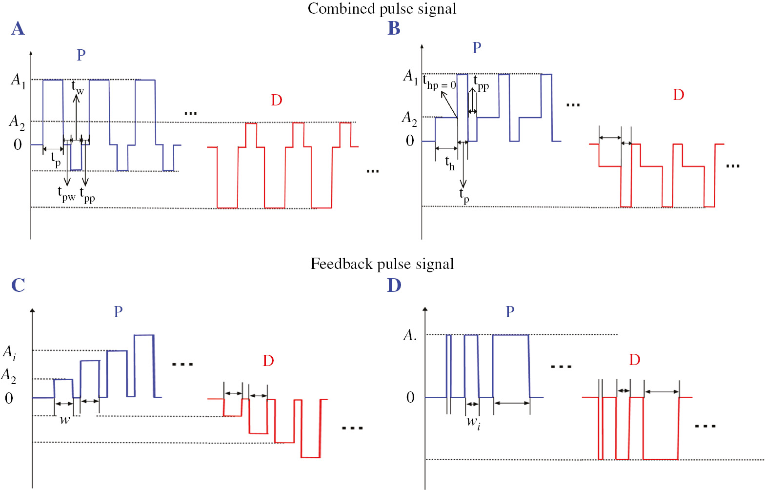
Abnormal pulse signal. (A) Combined pulse signal with the weak anti-pulse. (B) Combined pulse signal with the heating element. (C) Amplitude feedback pulse signal. (D) Width feedback pulse signal.
The combined pulse breaks the characteristic of a single pulse in a single cycle, and the small-amplitude pulse, called the weak pulse here, is attached with the programming pulse into one cycle as the extra stimulus signal. Figure 8A and B shows this kind of stimulating signal, and the weak pulse of different polarities has a different influence on the weight update of the memristor. When a weak signal is a polar opposite to the programming pulse, called the weak anti-pulse, the effect is to offset the ΔG caused by the programming pulse in the previous input cycle. On the contrary, when the weak signal is of the same polarity as the programming pulse, called the heating element, the weak signal is conducive to enhancing the particle diffusion in the device, thus, increasing the Gmax. As shown in Figure 8C and D, the feedback pulse uses feedback to process the amplitude and width of the stimulus signal in increments. Each feedback adjusts the next programming pulse according to the previous weight update results to obtain a conductance curve with the lowest NL value. The detail about these two kinds of programming pulse will be explained in sections 3.2.1 and 3.2.2. In schemes of stimulus signal, it is very important to note that the number of stimulus signal has no effect on the characteristic parameters of the memristor response. Enough stimulation cycle make the data more complete, more conducive to data processing and analyzing. According to the data expression of relevant references, the number of signal periods or the time of signal action is used as the abscissa cycle in the study of conductance modulation characteristics. In this review, the action of the cycle numbers is the same as that of the time as the Abscissa.
3.2.1 Combined pulse signal
3.2.1.1 The weak anti-pulse
Figure 8A shows a typical combined pulse signal, whose feature is the use of the weak pulses with opposite polarity (the weak anti-pulse) [60], [85], [120] to offset the abrupt ∆G caused by the training pulse in the first stage, which is the key of this scheme. In this scheme, training pulses are followed by pulses with lower amplitude and duration than the original pulse, whose polarity is opposite to that of the original pulse. It is feasible to achieve the NL optimization and preservation on an on/off ratio by taking the appropriate value of the conductance offset (Goffset), which is a concept pointed out by Wang et al. [85] in 2016. There is an equation that explains the relationship between real-time conductance (G(n)) and Goffset (Eq. (7)) [85]. In order to record the conductance value of the memristor after the effect of the previous programming pulse, reading pulses with very small amplitudes are applied after each programming pulse in the study. The number of pulses is used as the time axis to record the conductance value at the corresponding time. By processing the conductance value, and the difference conductance values, means that the ∆Gs of each state change are obtained. The ∆G is included in Eq. (7), in f(G), and the f(G) means a fit function related to the experimental results.
Eq. (7): G(n) is the conductance value after the nth pulse, Ginitial is the initial conductance before training, and Goffset is the offset value induced by the weak anti-pulse.
The reason why the pulse signal with the weak anti-pulse is useful in reducing the value of ∆G is that the weak anti-pulse can offset part of the accumulated charges, caused by the previous training pulse, at the interface between the electrodes and the RS layer, which results in the reduction of the electric field. The weakened electric field not only inhibits the process of ion drift but also suppresses the ions that are farther away from the CFs in the interface, and because of that the slope of conductance modulation curve in the first stage eventually becomes slower and slower (Figure 9A). The NL value, as defined in Eq. (1), of the identical programming pulse sequence, is about 0.6~0.81, which is about 0.42~0.54 of the optimized one. This result proves that the combined pulse signal with the weak anti-pulse has a practical significance for the optimization of NL. As shown in Figure 9B, both Gmax and NL are all infected by the value of Goffset. Goffset has a value of 0, which means that the identical pulse is applied to the memristor device as the stimulus signal. Goffset has a maximum value of 27 nS, because the maximum value of ∆G is 27nS when applied to the identical pulse. The conclusion drawn from Figure 9C is that the greater the value of Goffset is, the smaller is the NL of the device.
![Figure 9: Characteristics of the memristor response to the weak anti-pulse based on the 3D two-layer Ta/TaOx/TiO2/Ti memristor device. (A) Measured conductance modulation curves obtained by applying different pulse signal. Hollow point: response to the identical pulse. Solid point: response to the weak anti-pulse. Adapted with permission from [139]. Copyright 2016 Springer. (B) Simulated conductance modulation curves in different Goffset. (C) Relationship between Goffset and NL. Reprinted with permission from Ref. [139]. Copyright 2016 Springer.](/document/doi/10.1515/ntrev-2018-0045/asset/graphic/j_ntrev-2018-0045_fig_009.jpg)
Characteristics of the memristor response to the weak anti-pulse based on the 3D two-layer Ta/TaOx/TiO2/Ti memristor device. (A) Measured conductance modulation curves obtained by applying different pulse signal. Hollow point: response to the identical pulse. Solid point: response to the weak anti-pulse. Adapted with permission from [139]. Copyright 2016 Springer. (B) Simulated conductance modulation curves in different Goffset. (C) Relationship between Goffset and NL. Reprinted with permission from Ref. [139]. Copyright 2016 Springer.
The conclusion that should be drawn from the mentioned results is that in order to get the overall improvement of the properties of a memristor when optimizing on NL, it is very important to select the weak anti-pulse with appropriate parameters. In addition to the value of Goffset, the time interval between the weak anti-pulse and the programming pulse (tpw), the time interval between two pulse pairs (tpp) and the duration of the weak anti-pulse (tw) should all be considered as influencing factors in the optimization process. Considering that the energy consumption and the space of the system are pointed as the focus object when the researchers implement the neuromorphic calculation, the NL optimization of the memristor device should be as close as possible to this point. The implementation of this signal is not complicated, which only needs to use a two-pulse signal generator [85].
3.2.1.2 The heating element pulse
Figure 8B shows another kind of combined pulse signal, whose feature is the use of the weak pulses with the same polarity (the heating element) to enhance the particle diffusion process by rising the local temperature in the device bulk at the beginning of extra stimulation. Specifically, the pulse signal in this scheme consists of a heating element with lower amplitude and a programming element with a higher amplitude. The heating element will not lead to the RS process [85], and the RS behavior happens until the programming element arrives. Because of the considerations of temperature in the memristor device bulk in the second-order memristor model, the separation of stimulation signals for the two elements is considered as a kind of optimized scheme in NL.
The reason why this scheme works is that, in the case of applying an identical pulse on the device, the ions in the area near the CFs and farther away from the CFs are already exhausted, and the ions in the area far away from the CFs have difficulty in migrating to the area where the CFs are located, which limits further expansion of the CFs. However, in the case of applying a state-separated pulse, they promote the ions in the area far away from the CFs to migrate to the area where the CFs are located because of the enhanced diffusion process, which can further expand the CFs. The enhanced diffusion process is caused by a heating element, which leads to the local temperature rise. So the value of Gmax can be improved, and the NL can be optimized by the scheme here.
In this scheme, the frequency characteristics of the pulse pair signal are important. Among them, the time interval between the heating element and the programming element (thp), the time interval between two pulse pairs (tpp), and the width of heating element (th) are all considered as influencing factors in the optimized results. Only when thp is small enough does the heating element have a connection to the programming element, driving the memristor to a better state with higher conductance. Therefore, in Figure 8B, the thp is shown as zero. Figure 10A demonstrates that as the tpp decreases, the range of ΔG becomes larger, and the slope difference between the two-stage tends to be smaller. The th must be longer than or equal to the time constant [98], [104] of the device, which means the duration or time required for the device to reach a thermally stable state. The application of a heating element with the duration longer than the time constant would not lead to a further increase in local temperature and measurable differences in the RS behavior. However, the duration being shorter than the time constant would lead to the result that the heating element cannot complete the task of reducing NL to the maximum extent. Yeon Jeong et al. [104] applied the pulse signal involved in this section for the NL optimization results. The conductance modulation curve of the memristor device, stimulated by the pulse signal with heating element, has a higher value of Gmax and a smaller difference in slope than the one with identical pulse (Figure 10B).
![Figure 10: The response of the memristor to the pulse signal with different frequency characteristics. (A) Memristor conductance change as a function of the number and the frequency of the pulse. Adapted with permission from Ref. [98]. Copyright 2015 Nano letters. (B) Measured conductance modulation curves obtained by applying different pulse signals. Blue, the identical pulse; red, the pulse signal with the heating element. Inset shows the comparison of the difference between adjacent conductance when the device is programmed with the two kinds of programming schemes. Reprinted with permission from Ref. [104]. Copyright 2015 Applied Physics Letters.](/document/doi/10.1515/ntrev-2018-0045/asset/graphic/j_ntrev-2018-0045_fig_010.jpg)
The response of the memristor to the pulse signal with different frequency characteristics. (A) Memristor conductance change as a function of the number and the frequency of the pulse. Adapted with permission from Ref. [98]. Copyright 2015 Nano letters. (B) Measured conductance modulation curves obtained by applying different pulse signals. Blue, the identical pulse; red, the pulse signal with the heating element. Inset shows the comparison of the difference between adjacent conductance when the device is programmed with the two kinds of programming schemes. Reprinted with permission from Ref. [104]. Copyright 2015 Applied Physics Letters.
3.2.2 The feedback pulse signal
Another type of abnormal pulse signal is the one that is practically suitable, called the feedback pulse signal [15], [37], [48], [140], because it requires a complicated signal generation circuit as a peripheral circuit of the memristor device. However, it is worth noting that, in theory, it has the best optimization effect on the NL optimization problems (Figure 11). Neeraj et al. [131] showed in their article that the PCMO-based two-terminal memristor in their experiment had an NL of approximately 0 under pulsed feedback stimuli. Similar effects can be achieved with similar strategies based on the TaOx[41] memristor. Conductance of the memristor device obtained by applying an identical pulse is not predictable, as related to current conductance state. Therefore, the NL can be optimized by setting the parameters of the next programming pulse by judging the current response. The scheme in this section is called the programming scheme based on pulse feedback, which can be divided into the amplitude feedback pulse and the width feedback pulse. The purpose is to get a consistent ΔG by applying a training pulse sequence with different parameters in each pulse cycle, so that the slope of the conductance modulation curve tends to be consistent. A pulse with shorter duration (or lower amplitude) corresponds to a larger ΔG in the original scheme, and the pulse with a longer duration (or higher amplitude) corresponds to a smaller ΔG. Both the two strategies can achieve optimization on NL.
![Figure 11: Characteristics of the memristor response to the feedback pulse signal based on the TE/Al/PCMO/BE memristor device. Reprinted with permission from Ref. [139]. Copyright 2016 Springer. (A) Identical pulse. (B) Feedback pulse.](/document/doi/10.1515/ntrev-2018-0045/asset/graphic/j_ntrev-2018-0045_fig_011.jpg)
Characteristics of the memristor response to the feedback pulse signal based on the TE/Al/PCMO/BE memristor device. Reprinted with permission from Ref. [139]. Copyright 2016 Springer. (A) Identical pulse. (B) Feedback pulse.
For its shortage on complex peripheral circuits, at least one additional computing unit and a special signal generator are needed to comply with the input. A system with a synaptic array cannot achieve parallel weight updates because of feedback. Therefore, the space occupied, the circuit delay, and the energy consumption of the system will be significantly increased, which is not conducive to achieve a large-scale system. Only in theory, have these kinds of schemes any research value.
4 Memristor with the multi-RS layer
The original memristor had a simple sandwich structure that contained only one dielectric layer and only one kind of element except the element oxygen or the element nitrogen. Although the traditional structure is easy to implement in the process, it cannot achieve the desired performance for the current pursuit of device optimization. With the development of research, researchers tend to make a dielectric layer diversification by doping or making a multi-layer. The same approach is used in the NL optimization direction, and the desired effect can also be achieved. Xiao et al. [114] had different experimental results by doping in the RS layer. Matveyev et al. [10], [90] got it by making a multi RS layer. Gaba et al. [123] got it by making a multi RS layer, too. With the deepening of research, it has been gradually found that two or three layers of different kinds of dielectric layers have various degrees of optimization effects on the performance of the device. The use of materials with different oxygen contents as a component of the multi-RS layer has proven to be effective in confining the location where the CFs break down to smaller areas in the device bulk so that the performance of the device especially the stability is improved. A similar approach can be achieved on the issue of NL optimization. The difference is that in the NL optimization problem, from a material point of view, researchers need to consider the particle migration state inside, including drift speed and thermal diffusion. The combination of materials have different particle migration effects as the multi-RS layer of the device is verified to achieve the goal of controlling the device conductance distribution [102], [141], [142].
In detail, from Eqs. (2) and (3) derived from the Mott theory, particle migration is largely affected by the environment where the particles are located [143], [144]. Therefore, it is feasible to reduce the number of particles that participate at the beginning of conductance modulation by limiting the rate of particle migration, to achieve the purpose of slowing down the process of forming complete CFs. A viable program is to insert one or more layers with materials that can suppress particles migrating between the basic RS layer and the top electrode (Figure 12). Layers inserted are called the migration limit layer (MLL). Zongwei et al. [36] named their insert layer as an ion diffusion-limiting layer (DLL).
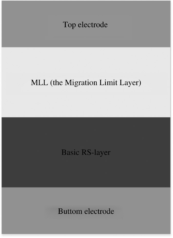
Model of the memristor with the MLL.
The PDE model shows that in the set process, under the stimulation of a directed external voltage, the jdrift and jdiff are in the same direction at the beginning, and the diffusion process promotes more particles to participate in the process of CF completeness. With the extension of stimulation time, due to the gradient distribution of the carrier concentration, the direction of jdiff is perpendicular to the direction of jdrift, as shown in Figure 5, resulting in the horizontal expansion of the CFs. The main influence of the drift process is the applied voltage stimulus. Therefore, from a material point of view, by controlling the diffusion process, the number of particles that previously participated in the RS process at the beginning can be limited. The purpose of doing so is to depress the high slope of the conductance modulation curve in the first stage, prompting NL optimization.
From the equation D=D0 exp (−Ea/kT) for the diffusion coefficient, the diffusion coefficient of oxygen (Dv) can be obtained. The materials of the MLL tend to choose the one with Dv less than that of the basic RS layer to achieve the NL optimization. In addition to the temperature of the device bulk, the two main influencing factors for Dv are “a” and “Ea”. The former is usually assumed in the calculation, the hypothesis is set at 0.05 nm ~0.5 nm [56], and the final simulated value depending on the fitting results of the calculation data and experiment data. “a” appears as a hypothetical value in the calculation. In the PDEs model ignoring the effect of the electrode heat release on the temperature in the device bulk, Kim et al. [56] drew a set of conclusions based on a series of reasonable assumptions, excluding the effect of electrode heat release on the temperature in the device. The calculation curves in the conclusion show that the larger the value of a, the more the device tends to be digitized, which means the larger the NL degree. This trend is unfavorable to the application in the field of the neuromorphic system. Table 3 lists the hypothetical values used in the calculation of several materials for reference. The latter is the activation energy for the hopping process, and the greater its value, the harder it is for the particles in the material to transition. Similarly, Table 3 lists the values of Ea for several materials. SiO2 is a typical semiconductor material with an Ea value in the range of 0.92 eV–1.71 eV and an average level higher than the other oxide semiconductors in Table 3. The Dv of SiO2 is about 10−24–10−20 cm2/s [55], [72] at room temperature, which is one or more orders of magnitude lower than that of other binary metal oxides. For example, it is lower by one to six orders of magnitude compared to TaOx[140], [149]. Zongwei et al. [36] inserted SiO2 as the MLL on the basic layer of TaOx in a memristor device. After comparing the memristor devices with different thicknesses of SiO2 (1 nm, 2 nm, 4 nm), they concluded that the NL of the device is obviously optimized when the MLL of SiO2 is 2 nm (Figure 13).
Summarization of diffusion constants of some dielectric layers corresponding to an oxygen.
| Assumption value | Material | Reference |
|---|---|---|
| a (nm) | ||
| 0.1 | TaOx | [56] |
| 0.1 | HfOx | [94] |
| 0.15 | WOx | [145] |
| 0.3 | Al2O3 | [146] |
| – | ||
| Ea (eV) | ||
| 0.4 | WOx | [145] |
| 0.85 | TaOx | [69] |
| 0.9 | Al2O3 | [146] |
| 1 | HfOx | [147], [148] |
| 0.92~1.71 | SiO2 | [69] |
![Figure 13: Conductance modulation curves obtained in memristive devices with SiO2 as the MLL with different thicknesses. Adapted with permission from Ref. [69]. Copyright 2016 Nanoscale. (A) TiN/1 nm-SiO2/TaOx/Pt memristor device. (B) TiN/2 nm-SiO2/TaOx/Pt memristor device. (C) TiN/4 nm-SiO2/TaOx/Pt memristor device. (D) TiN/TaOx/Pt memristor device, with no DLL.](/document/doi/10.1515/ntrev-2018-0045/asset/graphic/j_ntrev-2018-0045_fig_013.jpg)
Conductance modulation curves obtained in memristive devices with SiO2 as the MLL with different thicknesses. Adapted with permission from Ref. [69]. Copyright 2016 Nanoscale. (A) TiN/1 nm-SiO2/TaOx/Pt memristor device. (B) TiN/2 nm-SiO2/TaOx/Pt memristor device. (C) TiN/4 nm-SiO2/TaOx/Pt memristor device. (D) TiN/TaOx/Pt memristor device, with no DLL.
Finding the right kind of MLL material is the basis of NL optimization. In detail, the MLL with appropriate thickness can weaken the slope of the conductance modulation curve in the first stage, which is good for NL optimization. As shown in Figure 13A, when the thickness of SiO2 is 1 nm, the NL of the conductance modulation is significantly reduced, and the on/off ratio of the device is about 0.7, which is not too small compared with that of the device with no MLL. However, when the thickness is 4 nm, the Gmax is about 25% of the no MLL device, and the on/off ratio is only about 20%. As the thickness of the MLL increases, the length of the area where CF growth is limited increases. This results in an increase in the distance where particles need to move in a limited area. Over-thick MLL inhibits the diffusion process and the horizontal expansion process of the CFs in the memristor device. Therefore, the Gmax of the device is significantly reduced. Although the decrease in the Gmax will lead to a reduction in energy consumption of the device [96], there is a significant reduction in the on/off ratio, which is inconsistent with the purpose of device optimization. Furthermore, the SiO2 thin film formed by sputter deposition has a poor microscopic density compared with that formed by evaporation deposition [54]. The poor microscopic density results in a larger ion migration rate to give a more obvious effect on NL optimization.
5 Summary of the optimization scheme
The optimization schemes on the conductance modulation of the memristor in this review are mainly divided into two categories: applying a smarter programming pulse and changing the structure of the memristor. These schemes have different NL optimization effects, and there are differences in the ease of implementation. In order to make the paper more directive and intuitive, the advantages and disadvantages of the schemes are classified and summarized in this section. Objects are summarized in addition to the optimization schemes in the review and also those outside the scope of discussion but contributing to the direction of NL optimization. The above schemes are classified from three aspects: NL optimization, feasibility, and novelty degree.
For an identical pulse scheme, it is also possible to obtain a lower NL by changing the initial conductance, the pulse amplitude, or the pulse width. It is important to note that methods such as increasing the number of pulses have no effects on NL optimization. From a realizable point of view, uplifting the initial conductance can significantly reduce NL while largely reducing the on/off ratio. It is pointed out that optimizing NL by increasing the amplitude of the input pulse is useless, the results of which will be an increase in the maximum ΔG, not the NL optimization.
In the four kinds of pulse schemes mentioned above, the combined pulse schemes have obvious advantages over the feedback pulse schemes in terms of feasibility, which are mainly manifested in the stimulus signal generation module. The feedback schemes can get the most suitable stimulus signal by processing the response generated after each cycle and feeding back to the stimulus signal-generating module. Therefore, the complex stimulus signal generation and processing module is needed, and the feasibility is low. However, because of this, the feedback schemes can achieve almost an ideal NL optimization. Because the generating module of the stimulus signal requires extra consumption, the pulse scheme is weaker than the structural scheme in terms of feasibility and energy consumption. From the perspective of novelty, the pulse optimization scheme depends on the optimization of the three PDEs in theory. For example, the first-order memristor model is optimized to the second-order memristor model, which is dependent on T and w. It is of great significance to the performance optimization and theoretical model of the memristor.
Schemes with a multi-RS layer are immature; they has an advantage in simplifying the weight update process and the peripheral circuits compared to the other schemes, and it is feasible to achieve NL optimization by choosing suitable TE materials. In the aspect of feasibility, this scheme is superior to the pulse optimization schemes. The materials and structures of the RS layer of memristors are the main means of research in this field, which can achieve different optimization effects. Therefore, in these schemes, the novelty is attributed to the pulse optimization schemes.
This review focuses on memristors based on binary metal oxides, but there are also some related studies on NL optimization in the types of memristors outside this range. As shown in Table 2, it is worth noting that organic compound-based memristors, one of the main research directions of memristors, have NLs with excellent value, although their other aspects (like the on/off ratio) do not reach the same level as the metal oxide-based memristors. With the deepening of research, more and more research on memristors is using polymetallic oxides as materials of the RS layer, to achieve the goal of device optimization. Among them, Nili et al. from RMIT University conducted research on Nb-doping STO-based memristors [150]. In their research, Nb:a-STOx-based memristors show a high degree of uniformity and durability, and a lower NL of the conductance modulation results can be obtained by adjusting the partial bias amplitudes. It is worth noting that this study places the temperature and thermal effects of the device in an important position, which is the current research trend. As the upgrade structure of the two-terminal memristors, the three-terminal device [61], [63], [72], [73], [74], [75], [76], [77], [78] can achieve a good balance in NL optimization and other aspects, like energy consumption.
6 Application on neuromorphic learning
Synaptic circuits are used as a connection layer between two neuronal layers, which can use the memristor as the basic unit, to be components of a neuromorphic system [12], [151]. A hardware circuit system combines corresponding algorithms, like sparse coding algorithm, to achieve tasks [26], [138], [152], [153], [154], [155], [156], [157], [158] like image recognition. In the image recognition system, binary black and white images are made as the training objects. The system can store it after training, which means learning under stimulation from a training pulse.
In such an identification system, learning accuracy [11] is an important parameter to demonstrate the ability of such neuromorphic systems to accept and correctly identify what they learned, and conductance maps of the system can give a direct impression about it. The factors that may affect the learning accuracy include the NL of the weight update, the on/off ratio, and the device variations at the device level. In this section, the improvement of learning accuracy at the system level caused by optimized NL at the device level is analyzed.
Figure 14A shows the simulation results of a recognition system with 8×8 synapse cells [85]. The purpose of the system is to identify an 8×8 binary alphabetic “B” pattern with 10% error bits in each 8×8 training pattern. This indicates the initial state when the training period is 0. The initial weights of the synapses, which means the initial conductance of the synaptic memristors, are randomly distributed, as shown in Figure 14A. When the synaptic elements have an ideal linear weight update, the learning results gradually become obvious with an increase in the training cycles. After 60 training cycles, the learning process is completed with a learning accuracy of 100%, which has no error bit.
![Figure 14: Changes in learning accuracy at system level caused by optimized NL at device level. Adapted with permission from Ref. [139]. Copyright 2016 Springer. (A) Comparison of the simulated training weight map of an 8×8 binary alphabetic B pattern when the device is programmed with three weight update schemes. The first column, linear weight update scheme; the second column, scheme based on identical programming pulse; the third column, scheme based on the weak programming pulse with opposite polarity. (B) Comparison of the simulated training accuracy, defined by equation inset, when the device is programmed with three weight update schemes. Inset shows the difference in NL between two kinds of programming schemes (identical pulse, the weak pulse with opposite polarity).](/document/doi/10.1515/ntrev-2018-0045/asset/graphic/j_ntrev-2018-0045_fig_014.jpg)
Changes in learning accuracy at system level caused by optimized NL at device level. Adapted with permission from Ref. [139]. Copyright 2016 Springer. (A) Comparison of the simulated training weight map of an 8×8 binary alphabetic B pattern when the device is programmed with three weight update schemes. The first column, linear weight update scheme; the second column, scheme based on identical programming pulse; the third column, scheme based on the weak programming pulse with opposite polarity. (B) Comparison of the simulated training accuracy, defined by equation inset, when the device is programmed with three weight update schemes. Inset shows the difference in NL between two kinds of programming schemes (identical pulse, the weak pulse with opposite polarity).
When the synaptic elements are in the memristor device with a vertical double-layer structure based on tantalum oxide [159], the learning results are shown as fast close to saturation. However, the learning accuracy is only about 78% at the end of the stimulation, in which there are many error bits, as shown in Figure 14B. The reason for the higher learning outcome after the fifth training cycle, as shown in the second column in Figure 14A, can be attributed to the abrupt RS behavior of the synaptic device initially. As shown in Section 3, the scheme with the weak anti-pulse can reduce the NL level of the synaptic device by one level. The third column in Figure 14A shows the learning results based on this scheme. This shows a gradual situation, and the number of error bits is gradually reduced.
Compared with the learning accuracy based on the memristor synaptic devices with a different NL, it can be concluded that the learning accuracy of the system is affected by the NL of the device, as shown in Figure 14B.
However, optimization on NL would also change other performances [11] like the on/off ratio. Therefore, the above results can only indicate that the NL has an impact on the learning accuracy, but cannot explain which factor causes it specifically.
Figure 15A shows a map of the learning accuracy in a neuromorphic system [11] based on the NL-level table as shown in the inset of the graph. In the case of a perfectly symmetrical distribution of the LTP and LTD, when the NL level increases from 0 to 4, the learning accuracy of the system decreases gradually. When the NL level continues to rise to level 5, there is a slight increase in the learning accuracy. When it rises to level 6, there is a significant reduction in the learning accuracy. Figure 15B shows that in this system, when the on/off ratio of the device is reduced to less than 25, the learning accuracy of the system is significantly reduced. However, there is no obvious change. Although these results are based on a certain algorithm, we can give the following inspiration: (1) The on/off ratio of device has a threshold that determines the learning accuracy of the system. (2) There is a key point where NL is the main factor causing the learning accuracy optimization or deterioration.
![Figure 15: Chain effects caused by optimization on NL. (A) Comparison of the learning accuracy with different LTP and LTD non-linearities. Right, different non-linearity of the LTP and LTD fit from 0 to 6 and the level table about NL. Adapted with permission from Ref. [139]. Copyright 2016 Springer. (B) Learning accuracy with different on/off ratios. Reprinted with permission from Ref. [139]. Copyright 2016 Springer.](/document/doi/10.1515/ntrev-2018-0045/asset/graphic/j_ntrev-2018-0045_fig_015.jpg)
Chain effects caused by optimization on NL. (A) Comparison of the learning accuracy with different LTP and LTD non-linearities. Right, different non-linearity of the LTP and LTD fit from 0 to 6 and the level table about NL. Adapted with permission from Ref. [139]. Copyright 2016 Springer. (B) Learning accuracy with different on/off ratios. Reprinted with permission from Ref. [139]. Copyright 2016 Springer.
In summary, the NL of the weight update has direct and indirect effects on the learning accuracy of a neuromorphic system. The indirect effects are caused by the properties associated with NL. Optimized NL will inevitably change the other properties of the device, which will result in the improvement in the system learning accuracy.
7 Summary and prospect
Although there is no uniform standard for the RS mechanism yet, its scope has been gradually narrowing down along with more and more research about memristors turning up in recent years, and the non-ideal features of the memristor are more unignorable in the exploration of the RS mechanism. Especially, a lower NL of a conductance modulation is found to be helpful not only in establishing a mathematical model of the memristor with a higher fitting degree [67], [144], [159] but also in helping to improve the recognition accuracy of the neuromorphic system. The ultimate goal of doing optimization at the device level is to achieve systems with excellent performance. Based on this purpose, optimization on a device needs to find balance between all the associated properties.
Using the Mott theory and the three PDE models as a theoretical support for the RS process of the memristor device, we analyzed the reason for the NL based on the particle migration theory. Based on these theories, the formation process of the CFs inside the memristor has obvious stage phenomena. We do work summarizing the NL optimization scheme into two categories, applying smarter programming pulse and changing structure of the memristor, through the related experimental research, and analyzed their advantages.
The programming pulse signal has a significant influence on the CF formation process and internal temperature change and particle migration inside the memristor. In the aspect of NL optimization, the intensity parameters and timing parameters of a pulse signal have a certain influence on ΔG and Gmax. However, when the identical signals are as a stimulus, these parameters have no real impact on NL optimization. Therefore, the abnormal signals become more and more common in the related research. It is important to find a suitable extra pulse for the scheme for using the combined pulse signal. The design of this kind of signal is based on the three PDEs, and its experimental results can prove the correctness of the three PDEs while optimizing its solution process to obtain the simulation result with a higher fitting degree. The feedback pulse signal is another kind of optimization scheme, and it is achievable to obtain the optimal degree of NL using this programming pulse signal in the simulation. However, in the actual research, to realize this simulation physically, it is necessary to solve the problem of simplification of the complex degree of the signal-generation module, or the scheme has no practical application or value at the system level. NL optimization from the perspective of changing the component structure of the memristor has the same substantive effect. The main basis of this kind of scheme is to restrict the distance and speed of the particles moving inside the memristor by doping or MLL. One of the things that needs special attention in both scenarios is that changes in NL optimization may cause changes in its associated object, such as the on/off ratio or circuit complexity.
The final beneficiary for optimization at the device level should be the system. It is important to note that NL is an important factor that cannot be ignored in the field of application of neuromorphic systems, and we call it the relationship between the learning accuracy of the system, based on the memristor synaptic device, and the NL of the memristor. It has both a direct relationship and an indirect relationship. In the case of different systems and algorithms, NL has a different proportion of influence on learning accuracy, and its associated objects to the system will be different. It can be hypothesized that there are thresholds in NL optimization. When properties associated with the NL are lower than a threshold, NL optimization may be meaningless. At the system level, the stability, large-scale miniaturization, and low power consumption are the main research directions now. Therefore, optimization on a device must consider them. As regards NL optimization, doing optimization in the structure of the memristor is better considering space and energy. However, in both, the two categories of schemes in NL optimization, still more work that is valuable needs to be done in the future. Other non-ideal properties of the memristor also have limitations on its development and the neuromorphic system. Research on optimization needs to be continued in the future.
Funding source: National Natural Science Foundation of China
Award Identifier / Grant number: 51572041
Funding statement: This work was supported by Funds for International Science and Technology Cooperation of Sichuan 2017HH0052 and the National Natural Science Foundation of China 51572041, Funder Id: 10.13039/501100001809.
About the authors

Huan Liu is studying for a Master’s degree at the University of Electronic Science and Technology of China. She is doing research on the thin-film memristor, especially its optimization.

Min Wei received her PhD in 2012 from the University of Electronic Science and Technology of China. She was a visiting scholar in the University of California Santa Cruz from 2013 to 2014. Now, she is an Associate Professor in the University of Electronic Science and Technology of China. She is doing research on thin films and integrated devices.

Yuzhong Chen is studying for a Master’s degree in the University of Electronic Science and Technology of China. He is doing research on thin-film devices.
References
[1] Borghetti J, Li ZY, Straznicky J, Li XM, Ohlberg DAA, Wu W, Stewart DR, Williams RS. A hybrid nanomemristor/transistor logic circuit capable of self-programming. Proc. Natl. Acad. Sci. USA 2009, 106, 1699–1703.10.1073/pnas.0806642106Search in Google Scholar PubMed PubMed Central
[2] Yu SM, Gao B, Fang Z, Yu HY, Kang JF, Wong HSP. A neuromorphic visual system using RRAM synaptic devices with sub-pJ energy and tolerance to variability: experimental characterization and large-scale modeling. In 2012 IEEE International Electron Devices Meeting (IEDM), 2012.10.1109/IEDM.2012.6479018Search in Google Scholar
[3] Kuzum D, Jeyasingh RGD, Wong HSP. Energy efficient programming of nanoelectronic synaptic devices for large-scale implementation of associative and temporal sequence learning. In 2011 IEEE International Electron Devices Meeting (IEDM), 2011.10.1109/IEDM.2011.6131643Search in Google Scholar
[4] Suri M, Bichler O, Querlioz D, Palma G, Vianello E, Vuillaume D, Gamrat C, DeSalvo B. CBRAM devices as binary synapses for low-power stochastic neuromorphic systems: auditory (cochlea) and visual (retina) cognitive processing applications. In 2012 IEEE International Electron Devices Meeting (IEDM), 2012.10.1109/IEDM.2012.6479017Search in Google Scholar
[5] Strukov DB, Snider GS, Stewart DR, Williams RS. The missing memristor found. Nature 2008, 453, 80–83.10.1038/nature06932Search in Google Scholar PubMed
[6] Waser R, Dittmann R, Staikov G, Szot K. Redox-based resistive switching memories – nanoionic mechanisms, prospects, and challenges. Adv. Mater. 2009, 21, 2632–2663.10.1002/adma.200900375Search in Google Scholar
[7] Yang YC, Lu W. Nanoscale resistive switching devices: mechanisms and modeling. Nanoscale 2013, 5, 10076–10092.10.1039/c3nr03472kSearch in Google Scholar PubMed
[8] Yang JJS, Strukov DB, Stewart DR. Memristive devices for computing. Nat. Nanotechnol. 2013, 8, 13–24.10.1038/nnano.2012.240Search in Google Scholar PubMed
[9] Park S, Kim H, Choo M, Noh J, Sheri A, Jung S, Seo K, Park J, Kim S, Lee W, Shin J, Lee D, Choi G, Woo J, Cha E, Jang J, Park C, Jeon M, Lee B, Lee BH, Hwang H. RRAM-based synapse for neuromorphic system with pattern recognition function. In 2012 IEEE International Electron Devices Meeting (IEDM), 2012.10.1109/IEDM.2012.6479016Search in Google Scholar
[10] Matveyev Y, Kirtaev R, Fetisova A, Zakharchenko S, Negrov D, Zenkevich A. Crossbar nanoscale HfO2-based electronic synapses. Nanoscale Res. Lett. 2016, 11, 147.10.1186/s11671-016-1360-6Search in Google Scholar PubMed PubMed Central
[11] Chen PY, Lin BB, Wang IT, Hou TH, Ye JP, Vrudhula S, Seo JS, Cao Y, Yu SM. Mitigating effects of non-ideal synaptic device characteristics for on-chip learning. ICCAD-IEEE ACM Int. 2015, 194–199.10.1109/ICCAD.2015.7372570Search in Google Scholar
[12] Burr GW, Shelby RM, di Nolfo C, Jang JW, Shenoy RS, Narayanan P, Virwani K, Giacometti EU, Kurdi B, Hwang H. Experimental demonstration and tolerancing of a large-scale neural network (165,000 synapses), using phase-change memory as the synaptic weight element. In International Electron Devices Meeting (IEDM). 2014.10.1109/IEDM.2014.7047135Search in Google Scholar
[13] Yu SM, Chen PY, Cao Y, Xia LX, Wang Y, Wu HQ. Scaling-up resistive synaptic arrays for neuro-inspired architecture: challenges and prospect. In 2015 IEEE International Electron Devices Meeting (IEDM). 2015.10.1109/IEDM.2015.7409718Search in Google Scholar
[14] Izhikevich EM, Edelman GM. Large-scale model of mammalian thalamocortical systems. Proc. Natl. Acad. Sci. USA 2008, 105, 3593–3598.10.1073/pnas.0712231105Search in Google Scholar PubMed PubMed Central
[15] Indiveri G, Chicca E, Douglas R. A VLSI array of low-power spiking neurons and bistable synapses with spike-timing dependent plasticity. IEEE Trans. Neural Netw. 2006, 17, 211–221.10.1109/TNN.2005.860850Search in Google Scholar PubMed
[16] Bi GQ, Poo MM. Synaptic modifications in cultured hippocampal neurons: Dependence on spike timing, synaptic strength, and postsynaptic cell type. J. Neurosci. 1998, 18, 10464–10472.10.1523/JNEUROSCI.18-24-10464.1998Search in Google Scholar
[17] Li C, Min FH, Jin QS, Ma HY. Extreme multistability analysis of memristor-based chaotic system and its application in image decryption. AIP Adv. 2017, 7, 125204.10.1063/1.5006593Search in Google Scholar
[18] He WF, Sun HJ, Zhou YX, Lu K, Xue KH, Miao XS. Customized binary and multi-level HfO2-x-based memristors tuned by oxidation conditions. Sc.i Rep-UK 2017, 7, 10070.10.1038/s41598-017-09413-9Search in Google Scholar PubMed PubMed Central
[19] Su TY, Huang CH, Shih YC, Wang TH, Medina H, Huang JS, Tsai HS, Chueh YL. Tunable defect engineering in TiON thin films by multi-step sputtering processes: from a Schottky diode to resistive switching memory. J. Mater. Chem. C 2017, 5, 6319–6327.10.1039/C7TC01130JSearch in Google Scholar
[20] Merced-Grafals EJ, Davila N, Ge N, Williams RS, Strachan JP. Repeatable, accurate, and high speed multi-level programming of memristor 1T1R arrays for power efficient analog computing applications. Nanotechnology 2016, 27, 365202.10.1088/0957-4484/27/36/365202Search in Google Scholar PubMed
[21] Bass O, Fish A, Naveh D. A Memristor as multi-bit memory: feasibility analysis. Radioengineering 2015, 24, 425–430.10.13164/re.2015.0425Search in Google Scholar
[22] Park S, Sheri A, Kim J, Noh J, Jang J, Jeon M, Lee B, Lee BR, Lee BH, Hwang H. Neuromorphic speech systems using advanced ReRAM-based synapse. In 2013 IEEE International Electron Devices Meeting (IEDM), 2013.10.1109/IEDM.2013.6724692Search in Google Scholar
[23] Yu SM, Guan XM, Wong HSP. Understanding metal oxide RRAM current overshoot and reliability using kinetic Monte Carlo simulation. In 2012 IEEE International Electron Devices Meeting (IEDM), 2012.10.1109/IEDM.2012.6479105Search in Google Scholar
[24] Gao B, Bi YJ, Chen HY, Liu R, Huang P, Chen B, Liu L, Liu X, Yu S, Philip Wong H-S, Kang J. Ultra-Low-Energy Three-Dimensional Oxide-Based electronic synapses for implementation of robust high-accuracy neuromorphic computation systems. ACS Nano 2014, 8, 6998–7004.10.1021/nn501824rSearch in Google Scholar PubMed
[25] Chang T, Jo SH, Kim KH, Sheridan P, Gaba S, Lu W. Synaptic behaviors and modeling of a metal oxide memristive device. Appl. Phys. A-Mater. 2011, 102, 857–863.10.1007/s00339-011-6296-1Search in Google Scholar
[26] Jo SH, Chang T, Ebong I, Bhadviya BB, Mazumder P, Lu W. Nanoscale memristor device as synapse in neuromorphic systems. Nano Lett. 2010, 10, 1297–1301.10.1021/nl904092hSearch in Google Scholar PubMed
[27] Park SG, Yang MK, Ju H, Seong D-J, Lee JM, Kim E, Jung S, Zhang L, Shin YC, Baek I-G, Choi J, Kang H-K, Chung C. A non-linear ReRAM cell with sub-1 mu A ultralow operating current for high density vertical resistive memory (VRRAM). In 2012 IEEE International Electron Devices Meeting (IEDM), 2012.10.1109/IEDM.2012.6479084Search in Google Scholar
[28] Seo K, Kim I, Jung S, Jo M, Park S, Park J, Shin J, Biju KP, Kong J, Lee K, Lee B, Hwang H. Analog memory and spike-timing-dependent plasticity characteristics of a nanoscale titanium oxide bilayer resistive switching device. Nanotechnology 2011, 22, 254023.10.1088/0957-4484/22/25/254023Search in Google Scholar PubMed
[29] Prezioso M, Merrikh-Bayat F, Hoskins BD, Adam GC, Likharev KK, Strukov DB. Training and operation of an integrated neuromorphic network based on metal-oxide memristors. Nature 2015, 521, 61–64.10.1038/nature14441Search in Google Scholar PubMed
[30] Hong DS, Chen YS, Sun JR, Shen BG. Ternary synaptic plasticity arising from memdiode behavior of TiOx single nanowires. Adv. Electron. Mater. 2016, 2, 1500359.10.1002/aelm.201500359Search in Google Scholar
[31] Alamgir Z, Holt J, Beckmann K, Cady NC. The effect of different oxygen exchange layers on TaOx based RRAM devices. Semicond. Sci. Technol. 2018, 33, 0150114.10.1088/1361-6641/aa9a8fSearch in Google Scholar
[32] Du C, Ma W, Chang T, Sheridan P, Lu WD. Biorealistic Implementation of synaptic functions with oxide memristors through internal ionic dynamics. Adv. Funct. Mater. 2015, 25, 4290–4299.10.1002/adfm.201501427Search in Google Scholar
[33] Qu B, Younis A, Chu D. Recent progress in tungsten oxides based memristors and their neuromorphological applications. Electron. Mater. Lett. 2016, 12, 715–731.10.1007/s13391-016-6129-7Search in Google Scholar
[34] Wang IT, Lin YC, Wang YF, Hsu CW, Hou TH. 3D synaptic architecture with ultralow sub-10 fJ energy per spike for neuromorphic computation. In International Electron Devices Meeting (IEDM). 2014.10.1109/IEDM.2014.7047127Search in Google Scholar
[35] Li X, Wu H, Bin G, Wu W, Wu D, Deng N, Cai J, Qian H. Electrode-induced digital-to-analog resistive switching in TaO x-based RRAM devices. Nanotechnology 2016, 27, 305201.10.1088/0957-4484/27/30/305201Search in Google Scholar PubMed
[36] Wang ZW, Kang J, Yu ZZ, Fang YC, Ling YT, Cai YM, Huang R, Wang YY. Modulation of nonlinear resistive switching behavior of a TaOx-based resistive device through interface engineering. Nanotechnology 2017, 28, 055204.10.1088/1361-6528/28/5/055204Search in Google Scholar PubMed
[37] Lee MJ, Lee CB, Lee D, Lee SR, Chang M, Hur JH, Kim Y-B, Kim C-J, Seo DH, Seo S, Chung U-I, Yoo I-K, Kim K. A fast, high-endurance and scalable non-volatile memory device made from asymmetric Ta2O5−x/TaO2−x bilayer structures. Nat. Mater. 2011, 10, 625–630.10.1038/nmat3070Search in Google Scholar PubMed
[38] Yang JJ, Zhang MX, Strachan JP, Miao F, Pickett MD, Kelley RD, Medeiros-Ribeiro G, Williams RS. High switching endurance in TaOx memristive devices. Appl. Phys. Lett. 2010, 97, 232102.10.1063/1.3524521Search in Google Scholar
[39] Yang YC, Choi S, Lu W. Oxide heterostructure resistive memory. Nano Lett. 2013, 13, 2908–2915.10.1021/nl401287wSearch in Google Scholar PubMed
[40] Yang YC, Lee J, Lee S, Liu CH, Zhong ZH, Lu W. Oxide resistive memory with functionalized graphene as built-in selector element. Adv. Mater. 2014, 26, 3693–3699.10.1002/adma.201400270Search in Google Scholar PubMed
[41] Yang YC, Sheridan P, Lu W. Complementary resistive switching in tantalum oxide-based resistive memory devices. Appl. Phys. Lett. 2012, 100, 203112.10.1063/1.4719198Search in Google Scholar
[42] Wedig A, Luebben M, Cho DY, Moors M, Skaja K, Rana V, Hasegawa T, Adepalli KK, Yildiz B, Waser R, Valov I. Nanoscale cation motion in TaOx, HfOx and TiOx memristive systems. Nat. Nanotechnol. 2016, 11, 67–74.10.1038/nnano.2015.221Search in Google Scholar PubMed
[43] Suhas KA, Wang ZW, Huang XP, Kumari N, Davila N, Strachan JP, Vine D, David Kilcoyne AL, Nishi Y, Stanley R. Oxygen migration during resistance switching and failure of hafnium oxide memristors. Appl. Phys. Lett. 2017, 110, 103503.10.1063/1.4974535Search in Google Scholar
[44] Piccolboni G, Molas G, Garbin D, Vianello E, Cueto O, Cagli C, Traore B, De Salvo B, Ghibaudo G, Perniola L. Investigation of cycle-to-cycle variability in HfO2-Based OxRAM. IEEE Electron Device Lett. 2016, 37, 721–723.10.1109/LED.2016.2553370Search in Google Scholar
[45] Covi E, Brivio S, Serb A, Prodromakis T, Fanciulli M, Spiga S. HfO2-based memristors for neuromorphic applications. IEEE Int. Symp. Circ. S. 2016, 393–396.10.1109/ISCAS.2016.7527253Search in Google Scholar
[46] Jiang H, Han L, Lin P, Wang Z, Jang MH, Wu Q, Barnell M, Yang JJ, Xin HL, Xia Q. Sub-10 nm Ta channel responsible for superior performance of a HfO2 memristor. Sci. Rep. 2016, 6, 28525.10.1038/srep28525Search in Google Scholar PubMed PubMed Central
[47] Murdoch BJ, McCulloch DG, Ganesan R, McKenzie DR, Bilek MMM, Partridge JG. Memristor and selector devices fabricated from HfO2−xNx. Appl. Phys. Lett. 2016, 108, 143504.10.1063/1.4945727Search in Google Scholar
[48] Yan ZB, Liu JM. Resistance switching memory in perovskite oxides. Ann. Phys.-New York. 2015, 358, 206–224.10.1016/j.aop.2015.03.028Search in Google Scholar
[49] Wu ML, Yang CP, Shi DW, Wang RL, Xu LF, Xiao HB, Baerner K. Electric-pulse-induced resistance switching effect in the bulk of La0.5Ca0.5MnO3 ceramics. AIP Adv. 2014, 4, 047123.10.1063/1.4872216Search in Google Scholar
[50] Zhuge F, Li K, Fu B, Zhang H, Li J, Chen H, Liang L, Gao J, Cao H, Liu Z, Luo H. Mechanism for resistive switching in chalcogenide-based electrochemical metallization memory cells. AIP Adv. 2015, 5, 057125.10.1063/1.4921089Search in Google Scholar
[51] Ohno T, Hasegawa T, Tsuruoka T, Terabe K, Gimzewski JK, Aono M. Short-term plasticity and long-term potentiation mimicked in single inorganic synapses. Nat. Mater. 2011, 10, 591–595.10.1038/nmat3054Search in Google Scholar PubMed
[52] Shigeoka Y, Tsuruoka T, Hasegawa T. The rate limiting process and its activation energy in the forming process of a Cu/Ta2O5/Pt gapless-type atomic switch. Jpn. J. Appl. Phys. 2018, 57, 035202.10.7567/JJAP.57.035202Search in Google Scholar
[53] Bousoulas P, Giannopoulos I, Asenov P, Karageorgiou I, Tsoukalas D. Investigating the origins of high multilevel resistive switching in forming free Ti/TiO2−x-based memory devices through experiments and simulations. J. Appl. Phys. 2017, 121, 094501.10.1063/1.4977063Search in Google Scholar
[54] Yang Y, Gao P, Li L, Pan X, Tappertzhofen S, Choi S, Waser R, Valov I, Lu WD. Electrochemical dynamics of nanoscale metallic inclusions in dielectrics. Nat. Commun. 2014, 5, 4232.10.1038/ncomms5232Search in Google Scholar PubMed
[55] Yang Y, Gao P, Gaba S, Chang T, Pan X, Lu W. Observation of conducting filament growth in nanoscale resistive memories. Nat. Commun. 2012, 3, 732.10.1038/ncomms1737Search in Google Scholar PubMed
[56] Kim S, Choi S, Lu W. Comprehensive physical model of dynamic resistive switching in an oxide memristor. ACS Nano 2014, 8, 2369–2376.10.1021/nn405827tSearch in Google Scholar PubMed
[57] Kim S, Kim SJ, Kim KM, Lee SR, Chang M, Cho E, Kim Y-B, Kim CJ, Chung U-I, Yoo I-K. Physical electro-thermal model of resistive switching in bi-layered resistance-change memory. Sci. Rep. 2013, 3, 1680.10.1038/srep01680Search in Google Scholar PubMed PubMed Central
[58] Nardi F, Balatti S, Larentis S, Ielmini D. Complementary switching in metal oxides: toward diode-less crossbar RRAMs. In 2011 IEEE International Electron Devices Meeting (IEDM), 2011.10.1109/IEDM.2011.6131647Search in Google Scholar
[59] Kim S, Choi B, Lim M, Yoon J, Lee J, Kim HD, Choi SJ. Pattern recognition using carbon nanotube synaptic transistors with an adjustable weight update protocol. ACS Nano 2017, 11, 2814–2822.10.1021/acsnano.6b07894Search in Google Scholar PubMed
[60] Kim S, Choi S, Lee J, Lu WD. Tuning resistive switching characteristics of tantalum oxide memristors through Si doping. ACS Nano 2014, 8, 10262–10269.10.1021/nn503464qSearch in Google Scholar PubMed
[61] Zhu J, Yang Y, Jia R, Liang Z, Zhu W, Rehman ZU, Bao L, Zhang X, Cai Y, Song L, Huang R. Ion gated synaptic transistors based on 2D van der Waals crystals with tunable diffusive dynamics. Adv. Mater. (Deerfield Beach, Fla.). 2018, 30, 1800195.10.1002/adma.201800195Search in Google Scholar PubMed
[62] Kim S, Kim H, Jung S, Kim MH, Lee SH, Cho S, Park BG. Tuning resistive switching parameters in Si3N4-based RRAM for three-dimensional vertical resistive memory applications. J. Alloy Compd. 2016, 663, 419–423.10.1016/j.jallcom.2015.10.142Search in Google Scholar
[63] Kim S, Lim M, Kim Y, Kim HD, Choi SJ. Impact of synaptic device variations on pattern recognition accuracy in a hardware neural network. Sci. Rep.-UK 2018, 8, 2638.10.1038/s41598-018-21057-xSearch in Google Scholar PubMed PubMed Central
[64] Thomas A, Niehorster S, Fabretti S, Shepheard N, Kuschel O, Kupper K, Wollschlager J, Krzysteczko P, Chicca E. Tunnel junction based memristors as artificial synapses. Front. Neurosci. 2015, 9, 241.10.3389/fnins.2015.00241Search in Google Scholar PubMed PubMed Central
[65] Zhu X, Du C, Jeong Y, Lu WD. Emulation of synaptic metaplasticity in memristors. Nanoscale 2017, 9, 45–51.10.1039/C6NR08024CSearch in Google Scholar
[66] Kaveh M, Mott NF. Metal-insulator-transition near a superconducting state. Phys. Rev. Lett. 1992, 68, 1904–1907.10.1103/PhysRevLett.68.1904Search in Google Scholar PubMed
[67] Wang YF, Lin YC, Wang IT, Lin TP, Hou TH. Characterization and modeling of nonfilamentary Ta/TaOx/TiO2/Ti analog synaptic device. Sci. Rep.-UK 2015, 5, 10150.10.1038/srep10150Search in Google Scholar PubMed PubMed Central
[68] Wang LG, Zhang W, Chen Y, Cao YQ, Li AD, Wu D. Synaptic plasticity and learning behaviors mimicked in single inorganic synapses of Pt/HfOx/ZnOx/TiN memristive system. Nanoscale Res. Lett. 2017, 12, 65.10.1186/s11671-017-1847-9Search in Google Scholar PubMed PubMed Central
[69] Wang Z, Yin M, Zhang T, Cai Y, Wang Y, Yang Y, Huang R. Engineering incremental resistive switching in TaOx based memristors for brain-inspired computing. Nanoscale 2016, 8, 14015–14022.10.1039/C6NR00476HSearch in Google Scholar PubMed
[70] Zhang C, Tai Y-T, Shang J, Liu G, Wang K-L, Hsu C, Yi X, Yang X, Xue W, Tan H, Guo S, Pan L, Li R-W. Synaptic plasticity and learning behaviours in flexible artificial synapse based on polymer/viologen system. J. Mater. Chem. C 2016, 4, 3217–3223.10.1039/C6TC00496BSearch in Google Scholar
[71] Gou GY, Sun J, Qian C, He YK, Kong LA, Fu Y, Dai GZ, Yang JL, Gao YL. Artificial synapses based on biopolymer electrolyte-coupled SnO2 nanowire transistors. J. Mater. Chem. C.2016, 4, 11110–11117.10.1039/C6TC03731CSearch in Google Scholar
[72] He Y, Sun J, Qian C, Kong L-A, Gou G, Li H. Oxide-based synaptic transistors gated by solution-processed gelatin electrolytes. Appl. Phys. A. 2017, 123, 277.10.1007/s00339-017-0917-2Search in Google Scholar
[73] Diorio C, Hasler P, Minch A, Mead CA. A single-transistor silicon synapse. IEEE Trans. Electron Devices 1996, 43, 1972–1980.10.1109/16.543035Search in Google Scholar
[74] Agnus G, Zhao WS, Derycke V, Filoramo A, Lhuillier Y, Lenfant S, Vuillaume D, Gamrat C, Bourgoin JP. Two-terminal carbon nanotube programmable devices for adaptive architectures. Adv. Mater. 2010, 22, 702–706.10.1002/adma.200902170Search in Google Scholar PubMed
[75] Akinaga H, Shima H. Resistive random access memory (ReRAM) based on metal oxides. Proc. IEEE. 2010, 98, 2237–2251.10.1109/JPROC.2010.2070830Search in Google Scholar
[76] Lai QX, Zhang L, Li ZY, Stickle WF, Williams RS, Chen Y. Ionic/electronic hybrid materials integrated in a synaptic transistor with signal processing and learning functions. Adv. Mater. 2010, 22, 2448–2453.10.1002/adma.201000282Search in Google Scholar PubMed
[77] Han N, Park MU, Yoo KH. Memristive switching in Bi(1-x)Sb(x) nanowires. ACS Appl. Mater. Interfaces 2016, 8, 9224–9230.10.1021/acsami.6b01050Search in Google Scholar PubMed
[78] Yang X, Fang Y, Yu Z, Wang Z, Zhang T, Yin M, Lin M, Yang Y, Cai Y, Huang R. Nonassociative learning implementation by a single memristor-based multi-terminal synaptic device. Nanoscale 2016, 8, 18897–18904.10.1039/C6NR04142FSearch in Google Scholar PubMed
[79] Das M, Kumar A, Singh R, Htay MT, Mukherjee S. Realization of synaptic learning and memory functions in Y2O3 based memristive device fabricated by dual ion beam sputtering. Nanotechnology 2018, 29, 055203.10.1088/1361-6528/aaa0ebSearch in Google Scholar PubMed
[80] Banerjee W, Liu Q, Lv HB, Long SB, Liu M. Electronic imitation of behavioral and psychological synaptic activities using TiOx/Al2O3-based memristor devices. Nanoscale 2017, 9, 14442–14450.10.1039/C7NR04741JSearch in Google Scholar
[81] Jeong DS, Kim KM, Kim S, Choi BJ, Hwang CS. Memristors for energy-efficient new computing paradigms. Adv. Electron. Mater. 2016, 2, 1600090.10.1002/aelm.201600090Search in Google Scholar
[82] Ranjan R, Ponce PM, Hellweg WL, Kyrmanidis A, Abu Saleh L, Schroeder D, Krautschneider WH. Integrated circuit with memristor emulator array and neuron circuits for biologically inspired neuromorphic pattern recognition. J. Circuit Syst. Comp. 2017, 26, 1750183.10.1142/S0218126617501833Search in Google Scholar
[83] Qu B, Du HW, Wan T, Lin X, Younis A, Chu DW. Synaptic plasticity and learning behavior in transparent tungsten oxide-based memristors. Mater. Design. 2017, 129, 173–179.10.1016/j.matdes.2017.05.022Search in Google Scholar
[84] Cai WR, Ellinger F, Tetzlaff R. Neuronal synapse as a memristor: modeling pair- and triplet-based STDP rule. IEEE Trans. Biomed. Circ. S. 2015, 9, 87–95.10.1109/TBCAS.2014.2318012Search in Google Scholar PubMed
[85] Wang IT, Chang CC, Chiu LW, Chou T, Hou TH. 3D Ta/TaOx/TiO2/Ti synaptic array and linearity tuning of weight update for hardware neural network applications. Nanotechnology 2016, 27, 365204.10.1088/0957-4484/27/36/365204Search in Google Scholar PubMed
[86] Prezioso M, Merrikh Bayat F, Hoskins B, Likharev K, Strukov D. Self-adaptive spike-time-dependent plasticity of metal-oxide memristors. Sci. Rep. 2016, 6, 21331.10.1038/srep21331Search in Google Scholar PubMed PubMed Central
[87] Prezioso M, Zhong Y, Gavrilov D, Merrikh-Bayat F, Hoskins B, Adam G, Likharev K, Strukov D. Spiking neuromorphic networks with metal-oxide memristors. IEEE Int. Symp. Circ. S. 2016, 177–180.10.1109/ISCAS.2016.7527199Search in Google Scholar
[88] Chakrabarti B, Lastras-Montano MA, Adam G, Prezioso M, Hoskins B, Cheng KT, Strukov DB. A multiply-add engine with monolithically integrated 3D memristor crossbar/CMOS hybrid circuit. Sci. Rep.-UK 2017, 7, 42429.10.1038/srep42429Search in Google Scholar PubMed PubMed Central
[89] Egorov KV, Kirtaev RV, Lebedinskii YY, Markeev AM, Matveyev YA, Orlov OM, Zablotskiy AV, Zenkevich AV. Complementary and bipolar regimes of resistive switching in TiN/HfO2/TiN stacks grown by atomic-layer deposition. Phys. Status Solidi (A) 2015, 212, 809–816.10.1002/pssa.201431674Search in Google Scholar
[90] Matveyev Y, Egorov K, Markeev A, Zenkevich A. Resistive switching and synaptic properties of fully atomic layer deposition grown TiN/HfO2/TiN devices. J. Appl. Phys. 2015, 117, 044901.10.1063/1.4905792Search in Google Scholar
[91] Negrov D, Karandashev I, Shakirov V, Matveyev Y, Dunin-Barkowski W, Zenkevich A. An approximate backpropagation learning rule for memristor based neural networks using synaptic plasticity. Neurocomputing 2017, 237, 193–199.10.1016/j.neucom.2016.10.061Search in Google Scholar
[92] Sung C, Lim S, Kim H, Kim T, Moon K, Song J, Kim JJ, Hwang H. Effect of conductance linearity and multi-level cell characteristics of TaOx-based synapse device on pattern recognition accuracy of neuromorphic system. Nanotechnology 2018, 29, 115203.10.1088/1361-6528/aaa733Search in Google Scholar PubMed
[93] Garbin D, Rafhay Q, Vianello E, Jeannot S, Candelier P, DeSalvo B, Ghibaudo G, Perniola L. Modeling of OxRAM variability from low to high resistance state using a stochastic trap assisted tunneling-based resistor network. In 2015 Joint International Eurosoi Workshop and International Conference on Ultimate Integration on Silicon (Eurosoi-Ulis), 2015, pp. 125–128.10.1109/ULIS.2015.7063789Search in Google Scholar
[94] Mott NF, Gurney RW. Electronic processes in ionic crystals, 2nd ed., Clarendon Press: Oxford, 1948.Search in Google Scholar
[95] Larentis S, Nardi F, Balatti S, Gilmer DC, Ielmini D. Resistive switching by voltage-driven ion migration in bipolar RRAM – part II: modeling. IEEE Trans. Electron Devices. 2012, 59, 2468–2475.10.1109/TED.2012.2202320Search in Google Scholar
[96] Niraula D, Karpov VG. Heat transfer in filamentary RRAM devices. IEEE Trans. Electron Devices 2017, 64, 4106–4113.10.1109/TED.2017.2741782Search in Google Scholar
[97] Sadi T, Mehonic A, Montesi L, Buckwell M, Kenyon A, Asenov A. Investigation of resistance switching in SiOx RRAM cells using a 3D multi-scale kinetic Monte Carlo simulator. J. Phys.-Condens. Mater. 2018, 30, 084005.10.1088/1361-648X/aaa7c1Search in Google Scholar PubMed
[98] Kim S, Du C, Sheridan P, Ma W, Choi S, Lu WD. Experimental demonstration of a second-order memristor and its ability to biorealistically implement synaptic plasticity. Nano Lett. 2015, 15, 2203–2211.10.1021/acs.nanolett.5b00697Search in Google Scholar PubMed
[99] Xiao M, Shen DZ, Musselman KP, Duley WW, Zhou YN. Oxygen vacancy migration/diffusion induced synaptic plasticity in a single titanate nanobelt. Nanoscale 2018, 10, 6069–6079.10.1039/C7NR09335GSearch in Google Scholar PubMed
[100] Kumar S, Davila N, Wang ZW, Huang XP, Strachan JP, Vine D, Kilcoyne ALD, Nishi Y, Williams RS. Spatially uniform resistance switching of low current, high endurance titanium-niobium-oxide memristors. Nanoscale 2017, 9, 1793–1798.10.1039/C6NR07671HSearch in Google Scholar
[101] Molina-Reyes J, Hernandez-Martinez L. Understanding the resistive switching phenomena of stacked Al/Al2O3/Al thin films from the dynamics of conductive filaments. Complexity 2017, 8263904.10.1155/2017/8263904Search in Google Scholar
[102] Strukov DB, Alibart F, Williams R. Thermophoresis/diffusion as a plausible mechanism for unipolar resistive switching in metal-oxide-metal memristors. Appl. Phys. A-Mater. 2012, 107, 509–518.10.1007/s00339-012-6902-xSearch in Google Scholar
[103] Bricalli A, Ambrosi E, Laudato M, Maestro M, Rodriguez R, Ielmini D. Resistive switching device technology based on silicon oxide for improved ON-OFF ratio – part I: memory devices. IEEE Trans. Electron Devices 2018, 65, 115–121.10.1109/TED.2017.2777986Search in Google Scholar
[104] Jeong Y, Kim S, Lu WD. Utilizing multiple state variables to improve the dynamic range of analog switching in a memristor. Appl. Phys. Lett. 2015, 107, 173105.10.1063/1.4934818Search in Google Scholar
[105] Gao B, Liu L, Kang J. Investigation of the synaptic device based on the resistive switching behavior in hafnium oxide. Prog. Nat. Sci. Mater. Int. 2015, 25, 47–50.10.1016/j.pnsc.2015.01.005Search in Google Scholar
[106] Jo SH, Lu W. CMOS compatible nanoscale nonvolatile resistance, switching memory. Nano Lett. 2008, 8, 392–397.10.1021/nl073225hSearch in Google Scholar PubMed
[107] Yang JJ, Pickett MD, Li XM, Ohlberg DAA, Stewart DR, Williams RS. Memristive switching mechanism for metal/oxide/metal nanodevices. Nat. Nanotechnol. 2008, 3, 429–433.10.1038/nnano.2008.160Search in Google Scholar PubMed
[108] Jo SH, Kim KH, Lu W. Programmable resistance switching in nanoscale two-terminal devices. Nano Lett. 2009, 9, 496–500.10.1021/nl803669sSearch in Google Scholar PubMed
[109] Liu M, Abid Z, Wang W, He XL, Liu Q, Guan WH. Multilevel resistive switching with ionic and metallic filaments. Appl. Phys. Lett. 2009, 94, 233106.10.1063/1.3151822Search in Google Scholar
[110] Hasegawa T, Ohno T, Terabe K, Tsuruoka T, Nakayama T, Gimzewski JK, Aono M. Learning abilities achieved by a single solid-state atomic switch. Adv. Mater. 2010, 22, 1831–1834.10.1002/adma.200903680Search in Google Scholar PubMed
[111] Choi SJ, Park GS, Kim KH, Cho S, Yang WY, Li XS, Moon JH, Lee KJ, Kim K. In situ observation of voltage-induced multilevel resistive switching in solid electrolyte memory. Adv. Mater. 2011, 23, 3272–3277.10.1002/adma.201100507Search in Google Scholar PubMed
[112] Zeng YJ, Twan SC, Wang KW, Huang HH, Hsu YB, Wang CY, Lan MY, Lee SW. Enhanced biocompatibility in anodic TaOx nanotube arrays. Nanoscale Res. Lett. 2017, 12, 557.10.1186/s11671-017-2325-0Search in Google Scholar PubMed PubMed Central
[113] Park Y, Lee JS. Artificial synapses with short- and long-term memory for spiking neural networks based on renewable materials. ACS Nano 2017, 11, 8962–8969.10.1021/acsnano.7b03347Search in Google Scholar PubMed
[114] Xiao SX, Xie XD, Wen SP, Zeng ZG, Huang TW, Jiang JH. GST-memristor-based online learning neural networks. Neurocomputing 2018, 272, 677–682.10.1016/j.neucom.2017.08.014Search in Google Scholar
[115] Tian H, Mi W, Zhao H, Mohammad MA, Yang Y, Chiu PW, Ren TL. A novel artificial synapse with dual modes using bilayer graphene as the bottom electrode. Nanoscale 2017, 9, 9275–9283.10.1039/C7NR03106HSearch in Google Scholar PubMed
[116] Shi T, Yin XB, Yang R, Guo X. Pt/WO3/FTO memristive devices with recoverable pseudo-electroforming for time-delay switches in neuromorphic computing. Phys. Chem. Chem. Phys. 2016, 18, 9338–9343.10.1039/C5CP07675GSearch in Google Scholar
[117] Menzel S, Waters M, Marchewka A, Bottger U, Dittmann R, Waser R. Origin of the ultra-nonlinear switching kinetics in oxide-based resistive switches. Adv. Funct. Mater. 2011, 21, 4487–4492.10.1002/adfm.201101117Search in Google Scholar
[118] Buscarino A, Fortuna L, Frasca M, Gambuzza LV, Sciuto G. Memristive chaotic circuits based on cellular nonlinear networks. Int. J. Bifurcat. Chaos 2012, 22, 1250070.10.1142/S0218127412500708Search in Google Scholar
[119] Yan XB, Zhao JH, Liu S, Zhou ZY, Liu Q, Chen JS, Liu XY. Memristor with Ag-cluster-doped TiO2 films as artificial synapse for neuroinspired computing. Adv. Funct. Mater. 2018, 28, 1705320.10.1002/adfm.201705320Search in Google Scholar
[120] Woo J, Moon K, Song J, Lee S, Kwak M, Park J, Hwang H. Improved synaptic behavior under identical pulses using AlOx/HfO2Bilayer RRAM array for neuromorphic systems. IEEE Electron Device Lett. 2016, 37, 994–997.10.1109/LED.2016.2582859Search in Google Scholar
[121] Woo J, Song J, Moon K, Lee S, Park J, Hwang H. Multilevel conductance switching of a HfO2 RRAM array induced by controlled filament for neuromorphic applications. In 2016 IEEE Silicon Nanoelectronics Workshop (Snw). 2016, 40–41.10.1109/SNW.2016.7577975Search in Google Scholar
[122] Mähne H, Wylezich H, Hanzig F, Slesazeck S, Rafaja D, Mikolajick T. Analog resistive switching behavior of Al/Nb2O5/Al device. Semicond. Sci. Technol. 2014, 29, 104002.10.1088/0268-1242/29/10/104002Search in Google Scholar
[123] Gaba S, Sheridan P, Du C, Lu W. 3-D vertical dual-layer oxide memristive devices. IEEE Trans. Electron Devices 2014, 61, 2581–2583.10.1109/TED.2014.2319814Search in Google Scholar
[124] Pan R, Li J, Zhuge F, Zhu L, Liang L, Zhang H, Gao J, Cao H, Fu B, Li K. Synaptic devices based on purely electronic memristors. Appl. Phys. Lett. 2016, 108, 013504.10.1063/1.4939436Search in Google Scholar
[125] Park J, Kwak M, Moon K, Woo J, Lee D, Hwang H. TiOx-based RRAM synapse with 64-levels of conductance and symmetric conductance change by adopting a hybrid pulse scheme for neuromorphic computing. IEEE Electron Device Lett. 2016, 37, 1559–1562.10.1109/LED.2016.2622716Search in Google Scholar
[126] Wang C, He W, Tong Y, Zhao R. Investigation and manipulation of different analog behaviors of memristor as electronic synapse for neuromorphic applications. Sci. Rep. 2016, 6, 22970.10.1038/srep22970Search in Google Scholar PubMed PubMed Central
[127] Li S, Zeng F, Chen C, Liu H, Tang G, Gao S, Song C, Lin Y, Pan F, Guo D. Synaptic plasticity and learning behaviours mimicked through Ag interface movement in an Ag/conducting polymer/Ta memristive system. J. Mater. Chem. C 2013, 1, 5292.10.1039/c3tc30575aSearch in Google Scholar
[128] Jang JW, Park S, Jeong YH, Hwang H. ReRAM-based synaptic device for neuromorphic computing. In 2014 IEEE International Symposium on Circuits and Systems (ISCAS), 2014, 1054–1057.10.1109/ISCAS.2014.6865320Search in Google Scholar
[129] Yang X, Wang C, Shang J, Zhang C, Tan H, Yi X, Pan L, Zhang W, Fan F, Liu Y, Chen Y, Liu G, Li R-W. An organic terpyridyl-iron polymer based memristor for synaptic plasticity and learning behavior simulation. RSC Adv. 2016, 6, 25179–25184.10.1039/C6RA02915ASearch in Google Scholar
[130] Zhang Y, Li Y, Wang X, Friedman EG. Synaptic characteristics of Ag/AgInSbTe/Ta-based memristor for pattern recognition applications. IEEE Trans. Electron Devices 2017, 64, 1806–1811.10.1109/TED.2017.2671433Search in Google Scholar
[131] Panwar N, Rajendran B, Ganguly U. Arbitrary spike time dependent plasticity (STDP) in memristor by analog waveform engineering. IEEE Electron Device Lett. 2017, 38, 740–743.10.1109/LED.2017.2696023Search in Google Scholar
[132] Balakrishna Pillai P, De Souza MM. Nanoionics-based three-terminal synaptic device using zinc oxide. ACS Appl. Mater. Interfaces 2017, 9, 1609–1618.10.1021/acsami.6b13746Search in Google Scholar PubMed
[133] Yan XB, Zhou ZY, Zhao JH, Liu Q, Wang H, Yuan GL, Chen JS. Flexible memristors as electronic synapses for neuro-inspired computation based on scotch tape-exfoliated mica substrates. Nano Res. 2018, 11, 1183–1192.10.1007/s12274-017-1781-2Search in Google Scholar
[134] Shouval HZ, Bear MF, Cooper LN. A unified model of NMDA receptor-dependent bidirectional synaptic plasticity. Proc. Natl. Acad. Sci. USA 2002, 99, 10831–10836.10.1073/pnas.152343099Search in Google Scholar PubMed PubMed Central
[135] Graupner M, Brunel N. Calcium-based plasticity model explains sensitivity of synaptic changes to spike pattern, rate, and dendritic location. Proc. Natl. Acad. Sci. USA 2012, 109, 3991–3996.10.1073/pnas.1109359109Search in Google Scholar PubMed PubMed Central
[136] Goodwill JM, Sharma AA, Li D, Bain JA, Skowronski M. Electro-thermal model of threshold switching in TaOx-based devices. ACS Appl. Mater. Int. 2017, 9, 11704–11710.10.1021/acsami.6b16559Search in Google Scholar PubMed
[137] Jeong Y, Zidan MA, Lu WD. Parasitic effect analysis in memristor-array-based neuromorphic systems. IEEE Trans. Nanotechnol. 2018, 17, 184–193.10.1109/TNANO.2017.2784364Search in Google Scholar
[138] Park S, Chu M, Kim J, Noh J, Jeon M, Lee BH, Hwang H, Lee B, Lee BG. Electronic system with memristive synapses for pattern recognition. Sci. Rep.-UK 2015, 5, 10123.10.1038/srep10123Search in Google Scholar PubMed PubMed Central
[139] Yu S. Neuro-inspired computing using resistive synaptic devices, Springer: Berlin, 2017.10.1007/978-3-319-54313-0Search in Google Scholar
[140] Kajihara K, Kamioka H, Hirano M, Miura T, Skuja L, Hosono H. Interstitial oxygen molecules in amorphous SiO2. III. Measurements of dissolution kinetics, diffusion coefficient, and solubility by infrared photoluminescence. J. Appl. Phys. 2005, 98, 013529.10.1063/1.1943506Search in Google Scholar
[141] Miao F, Strachan JP, Yang JJ, Zhang M-X, Goldfarb I, Torrezan AC, Eschbach P, Kelley RD, Medeiros-Ribeiro G, Williams RS. Anatomy of a nanoscale conduction channel reveals the mechanism of a high-performance memristor. Adv. Mater. 2011, 23, 5633–5640.10.1002/adma.201103379Search in Google Scholar PubMed
[142] Kumar S, Graves CE, Strachan JP, Kilcoyne ALD, Tyliszczak T, Nishi Y, Williams RS. In-operando synchronous time-multiplexed O K-edge x-ray absorption spectromicroscopy of functioning tantalum oxide memristors. J. Appl. Phys. 2015, 118, 034502.10.1063/1.4926477Search in Google Scholar
[143] Molina J, Torres R, Ranjan A, Pey KL. Resistive switching characteristics of MIM structures based on oxygen-variable ultra-thin HfO2 and fabricated at low temperature. Mater. Sci. Semicond. Proc. 2017, 66, 191–199.10.1016/j.mssp.2017.05.001Search in Google Scholar
[144] Hsu CW, Wang YF, Wan CC, Wang IT, Chou CT, Lai WL, Lee YJ, Hou TH. Homogeneous barrier modulation of TaOx/TiO2 bilayers for ultra-high endurance three-dimensional storage-class memory. Nanotechnology 2014, 25, 165202.10.1088/0957-4484/25/16/165202Search in Google Scholar PubMed
[145] Ho CH, Lai EK, Lee MD, Pan CL, Yao YD, Hsieh KY, Liu R, Lu CY. A highly reliable self-aligned graded oxide WOx resistance memory: conduction mechanisms and reliability. In 2007 Symposium on VLSI Technology, Digest of Technical Papers, 2007, 228–229.10.1109/VLSIT.2007.4339703Search in Google Scholar
[146] Sankaran K, Goux L, Clima S, Mees M, Kittl J, Jurczak M, Altimime L, Rignanese GM, Pourtois G. Modeling of copper diffusion in amorphous aluminum oxide in CBRAM stack. In Dielectrics for nanosystems 5: Materials Science, Processing, Reliability, and Manufacturing-and-Tutorials in Nanotechnology: More Than Moore – Beyond CMOS Emerging Materials and Devices 2012, 45, 317–330.10.1149/1.3700896Search in Google Scholar
[147] Yu S, Wong HSP. A phenomenological model for the reset mechanism of metal oxide RRAM. IEEE Electron Device Lett. 2010, 31, 1455–1457.10.1109/LED.2010.2078794Search in Google Scholar
[148] Kim HS, Sah MP, Yang CJ, Cho S, Chua LO. Memristor emulator for memristor circuit applications. IEEE Trans. Circuits-I 2012, 59, 2422–2431.10.1109/TCSI.2012.2188957Search in Google Scholar
[149] Kajihara K, Hirano M, Uramoto M, Morimoto Y, Skuja L, Hosono H. Interstitial oxygen molecules in amorphous SiO2. I. Quantitative concentration analysis by thermal desorption, infrared photoluminescence, and vacuum-ultraviolet optical absorption. J. Appl. Phys. 2005, 98, 013527.10.1063/1.1943504Search in Google Scholar
[150] Nili H, Ahmed T, Walia S, Ramanathan R, Kandjani AE, Rubanov S, Kim J, Kavehei O, Bansal V, Bhaskaran M, Sriraml S. Microstructure and dynamics of vacancy-induced nanofilamentary switching network in donor doped SrTiO3−x memristors. Nanotechnology 2016, 27, 505210.10.1088/0957-4484/27/50/505210Search in Google Scholar PubMed
[151] Kuzum D, Yu S, Wong HS. Synaptic electronics: materials, devices and applications. Nanotechnology 2013, 24, 382001.10.1088/0957-4484/24/38/382001Search in Google Scholar PubMed
[152] Li BX, Gu P, Shan Y, Wang Y, Chen YR, Yang HZ. RRAM-based analog approximate computing. IEEE Trans Comput. Aid Design 2015, 34, 1905–1917.10.1109/TCAD.2015.2445741Search in Google Scholar
[153] Querlioz D, Bichler O, Vincent AF, Gamrat C. Bioinspired programming of memory devices for implementing an inference engine. Proc. IEEE 2015, 103, 1398–1416.10.1109/JPROC.2015.2437616Search in Google Scholar
[154] Merolla PA, Arthur JV, Alvarez-Icaza R, Cassidy AS, Sawada J, Akopyan F, Jackson BL, Imam N, Guo C, Nakamura Y, Brezzo B, Vo I, Esser SK, Appuswamy R, Taba B, Amir A, Flickner MD, Risk WP, Manohar R, Modha DS. A million spiking-neuron integrated circuit with a scalable communication network and interface. Science 2014, 345, 668–673.10.1126/science.1254642Search in Google Scholar PubMed
[155] Merkel C, Kudithipudi D. Comparison of off-chip training methods for neuromemristive systems. In Int. Conference on VLSI Design. 2015, 99–104.10.1109/VLSID.2015.22Search in Google Scholar
[156] Gubicza A, Csontos M, Halbritter A, Mihaly G. Non-exponential resistive switching in Ag2S memristors: a key to nanometer-scale non-volatile memory devices. Nanoscale 2015, 7, 4394–4399.10.1039/C5NR00399GSearch in Google Scholar
[157] Werner T, Vianello E, Bichler O, Garbin D, Cattaert D, Yvert B, De Salvo B, Perniola L. Spiking neural networks based on OxRAM synapses for real-time unsupervised spike sorting. Front. Neurosci. 2016, 10, 474.10.3389/fnins.2016.00474Search in Google Scholar
[158] Covi E, Brivio S, Serb A, Prodromakis T, Fanciulli M, Spiga S. Analog memristive synapse in spiking networks implementing unsupervised learning. Front. Neurosci. 2016, 10, 482.10.3389/fnins.2016.00482Search in Google Scholar PubMed PubMed Central
[159] Guan X, Yu S, Wong HSP. A SPICE compact model of metal oxide resistive switching memory with variations. IEEE Electron Device Lett. 2012, 33, 1405–1407.10.1109/LED.2012.2210856Search in Google Scholar
©2018 Walter de Gruyter GmbH, Berlin/Boston
This article is distributed under the terms of the Creative Commons Attribution Non-Commercial License, which permits unrestricted non-commercial use, distribution, and reproduction in any medium, provided the original work is properly cited.
Articles in the same Issue
- Frontmatter
- In this issue
- Regular articles
- Simulation model for frictional contact of two elastic surfaces in micro/nanoscale and its validation
- Silver nanoparticles in the thermal silver plating of aluminium busbar joints
- Nanotechnology Education Contribution
- Insertion points of the essential nanoscale science and technology (NST) concepts in the Israeli middle school science and technology curriculum
- Reviews
- Recent progress in photodetectors based on low-dimensional nanomaterials
- Elemental zinc to zinc nanoparticles: is ZnO NPs crucial for life? Synthesis, toxicological, and environmental concerns
- Optimization of non-linear conductance modulation based on metal oxide memristors