Near-field refractometry of van der Waals crystals
-
Martin Nørgaard

 ,
Torgom Yezekyan
,
Stefan Rolfs
,
Christian Frydendahl
,
N. Asger Mortensen
and
Vladimir A. Zenin
,
Torgom Yezekyan
,
Stefan Rolfs
,
Christian Frydendahl
,
N. Asger Mortensen
and
Vladimir A. Zenin

Abstract
Common techniques for measuring refractive indices, such as ellipsometry and goniometry, are ineffective for van der Waals crystal flakes because of their high anisotropy and small, micron-scale, lateral size. To address this, we employ near-field optical microscopy to analyze the guided optical modes within these crystals. By probing these modes in MoS2 flakes with subwavelength spatial resolution at a wavelength of 1,570 nm, we determine both the in-plane and out-of-plane permittivity components of MoS2 as 16.11 and 6.25, respectively, with a relative uncertainty below 1 %, while overcoming the limitations of traditional methods.
1 Introduction
The discovery of the exceptional properties of graphene, enabled by a straightforward exfoliation technique to isolate monocrystalline graphitic films in the early 2000s [1], ignited a search for other materials with layered structures held together by weak van der Waals (vdW) forces. These materials, including transition metal dichalcogenides (TMDCs), have become a focal point in optoelectronics and quantum nanophotonics owing to their unique optical and electrical properties [2], [3], [4], [5]. Due to the layered structure of vdW materials, most of them are expected to exhibit giant anisotropy and even hyperbolic dispersion [6], which cannot be found among previously known naturally occurring materials. TMDCs, for instance, display remarkable optical behavior; their monolayers, readily exfoliated from bulk crystals [7], [8], [9], often exhibit optoelectronic properties distinctly different from those of their bulk counterparts [10], [11]. Molybdenum disulfide (MoS2), the TMDC considered in the present work, exemplifies this: it transitions from an indirect bandgap semiconductor with a 1.29 eV bandgap in bulk [12] to a direct bandgap semiconductor with a 1.8–1.9 eV bandgap as a monolayer [13], [14].
Theoretical and computational advancements [11], [15], [16], [17], [18] and experimental explorations [7], [14], [19], [20], [21] have propelled the understanding of vdW materials, yet the experimental characterization of their basic optical properties remains challenging. Exfoliated flakes are generally too small and non-uniform in thickness for traditional refractive index measurements, which limits precision in determining key optical parameters like the complex permittivity tensor. Understanding these optical properties is crucial for the design and optimization of devices based on vdW materials, such as metasurfaces [22], [23], [24], and could enable new applications previously limited by a lack of suitable materials with such unique properties.
Some refractive index measurement methods rely on Snell’s law and goniometer setups to precisely measure refraction angles; however, they are ineffective for slab-like samples, where refraction results only in slight beam displacement. Techniques such as measuring critical angles for total internal reflection or using Brewster’s angle provide rough estimations but lack accuracy due to weak angular dependence. The most advanced method, ellipsometry, measures the change in polarization upon reflection, which is fitted by different models to extract the thickness and refractive index of the unknown layer. However, the precision of conventional spectroscopic ellipsometry relies on using a well-collimated beam with a spot size of
In contrast to far-field methods, scanning near-field microscopy (SNOM) bypasses the issue of lateral resolution. It has been shown that one can use scattering-type (s-)SNOM to obtain quantitative measurements of local dielectric constants by the modification of the scattering strength of the s-SNOM probe by its environment. One approach is based on developing a rigorous model of the probe (a point dipole model, which was later modified into a finite dipole model), which is first applied on known samples for calibration, and then it can be used for measurements [32], [33]. Another approach is based on an empirical search for the probe response function from a set of calibration measurements (black-box calibration) [34], [35]. These methods allow for the extraction of permittivity without detailed electromagnetic modeling of the probe-sample interaction, even accounting for probe tapping effects and far-field background. However, they are developed for isotropic samples, making it challenging to apply them to highly anisotropic vdW materials. Moreover, to our knowledge, they cannot deal with samples where guided modes are excited.
Here we implemented a method we termed ‘near-field refractometry’, which works by probing guided modes within the material, whose properties are directly linked to the material optical properties [36], [37], [38], [39], [40]. Moreover, this approach demonstrated sensitivity to both in-plane and out-of-plane refractive index components, making it uniquely suited for measurements of highly anisotropic vdW materials. It has been shown that the s-SNOM imaging of propagating modes can be used to accompany and refine the far-field refractive index measurements [27], [30], [41]. We show that the optical constants can be precisely determined alone from the near-field measurements, when properly done.
We demonstrate the precision and accuracy of our method by investigating a highly anisotropic vdW material, namely MoS2 [27], using a phase-resolved SNOM (Figure 1a). We map the near field of guided modes within MoS2 flakes of finite thickness (Figure 1c and d) at photon energies below the bandgap (λ 0 = 1,570 nm), with a scan size as small as 40 μm by 20 μm (Figure 1b). First, the guided transverse electric (TE) and transverse magnetic (TM) modes are found by Fourier transforming the recorded near-field map (Figure 1e). After filtering in the Fourier domain, these modes are fitted in the direct space to extract their propagation constant. Finally, after collection of the thickness-dependent dispersion characteristics of these modes, we extract the anisotropic dielectric function of MoS2 and estimate its uncertainty.

Experimental scheme of the near-field refractometry setup. a) Artistic representation of the experiment where guided modes in an MoS2 flake are probed using a transmission s-SNOM setup. b) Differential interference contrast image of a t = 185 nm thick MoS2 flake. The scale bar is 20 μm. c-d) amplitude
2 Results
To illustrate the general concept of near-field refractometry of vdW materials, we first provide the electrodynamic theoretical foundation, followed by sample fabrication, near-field optical measurements, and data processing to eventually extract the anisotropic optical constants of the vdW material.
Planar thin-film waveguide modes. We consider a generic anisotropic dispersive dielectric function of a uniaxial vdW crystal flake
where ɛ ‖ and ɛ ⊥ are the in-plane and out-of-plane components, respectively. We assume that the flake of thickness t is resting on a substrate with dielectric function ɛ s (ω), while being exposed to air above the flake (ɛ a = 1). Given its high dielectric function (ɛ > ɛ s > ɛ a ), the flake is essentially a thin-film waveguide, supporting TE and TM modes, which are guided in-plane of the flake, along the x-axis, while being strongly localized in the out-of-plane direction (z-direction). The dispersion of TE modes is governed by
where
where
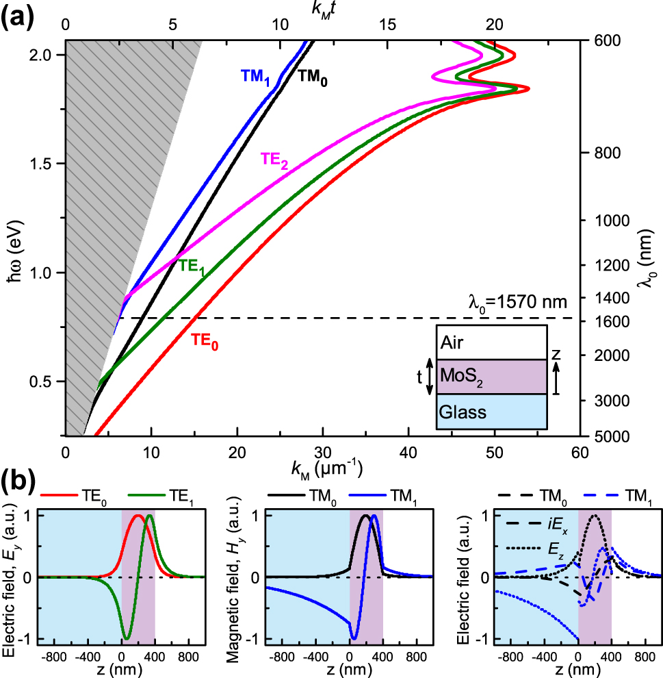
Planar thin-film waveguide modes. a) Dispersion diagram showing photon energy ℏω (left vertical axis) and corresponding free-space wavelength λ 0 (right vertical axis) versus mode propagation constant k M (horizontal axes) for a t = 400 nm MoS2 flake on BK7 glass substrate for selected TE m (m = 0, 1, 2) and TM m (m = 0, 1) modes. The regime of leaky substrate modes is gray shaded, while the horizontal dashed line indicates the experimentally used wavelength. b) Field profiles for the TE m and TM m modes (m = 0, 1), propagating along the x-axis.
At a specific photon energy ℏω (or wavelength λ
0 = 2π/k
0 = 2πc/ω), only certain guided modes are supported by the MoS2 flake. Adjusting the thickness t shifts the guided mode curves along the
Importantly, SNOM maps the evanescent field in the vicinity of the probe, therefore the mode confinement plays a crucial role in detecting the individual modes. We have calculated the mode profiles at λ 0 = 1,570 nm, which are depicted in Figure 2b. Since s-SNOM is most sensitive to the out-of-plane component of the electric field due to its elongated tip-based scattering probe, the signal of the TM modes will be the strongest, as they contain both E x and E z electric field components. In contrast, TE modes only have the E y field component. More details on the influence of the modes on the detectability is presented in the SI section S2.
Our proposed near-field refractometry method starts with measuring the complex-valued near-field maps of the guided modes, allowing accurate determination of the propagation constant k M (t) of each mode, which is then rigorously fitted to the above model, Equations (2a) and (2b), to eventually extract ɛ ‖ and ɛ ⊥.
Sample fabrication and pre-selection of flakes. We mechanically exfoliated MoS2 flakes with a modified ‘scotch tape’ method (see Methods section). Figure 1b shows a differential interference contrast image of one flake, revealing surface details not clearly visible in the bright- and dark-field images. However, all three complementary imaging methods were used to select flakes with a clean and uniformly thick area, suitable for the precise s-SNOM scanning. Another important aspect of the exfoliation technique used is that as MoS2 flakes become thicker, they tend to exhibit more folds and wrinkles, making it harder to obtain large, uniform, flat areas.
It is crucial to have a wide range of flake thicknesses, which should support several guided modes to reliably fit the data to Equations (2a)–(2b) and verify our model, as will be discussed later. For this purpose, we selected six different flakes (labeled from A through F) with the thicknesses varied from ca. 80 to 460 nm, as measured with atomic force microscopy (AFM), each with an estimated uncertainty of ± 10 %.
Furthermore, reflection spectroscopy of each flake can be used to estimate the thickness using the Fresnel equations for anisotropic media [42]; however, this requires a priori knowledge of ɛ(ω) over a wide range of frequencies.
For a detailed view of the MoS2 flake characterization, including optical microscopy and reflection spectroscopy, see the SI section S3.
Near-field measurements. Our s-SNOM setup can measure both the amplitude and the phase of the evanescent near field, enabling the complete mapping of the complex dispersion relation of guided modes. In our s-SNOM configuration, the light reaches the sample from the opposite side of the scattering tip, which is referred to as transmission-type [36], [37]. Unlike the commonly used reflection configuration [43], this transmission configuration conveniently separates the illumination and detection parts of the setup. This allows mapping the near field of guided modes ‘as launched’ from the edge of the MoS2 flakes, without taking the influence of the tip and geometrical decay into account. The concept of transmission s-SNOM is illustrated in Figure 1a, while Figure 1c and d present an example of the obtained near-field map, displayed as the electric near-field amplitude
In the experiments, a continuous-wave laser with a wavelength of λ
0 = 1,570 nm and a Gaussian beam profile is used as the light source. In this wavelength region, MoS2 is expected to have negligible optical loss [27], meaning that the drop in
For each scan, we choose an area that encompasses the entire beam along the y-axis and is sufficiently large along the x-axis to capture enough periods, resulting in a scan size of approximately 40 μm by 20 μm for all measurements. To avoid artifacts (aliasing) and distortion in the complex near-field data, the spatial sampling rate must exceed the Nyquist rate (f s > 2f max) for the highest spatial frequency (f max = k ‖/2π) measured along the propagation direction. To ensure that we resolve all modes for all thicknesses while maintaining consistency, a step size of 25 nm along the propagation direction is chosen for all measurements. Along the y-axis, we used a step size of 250 nm.
Data processing. To unambiguously extract the ‘pure’ or individual guided modes, the complex near-field maps are filtered to consider only one guided mode at a time. First, by applying a one-dimensional (1D) Fourier transform along the propagation direction (x → k x ) and averaging along the columns (y-axis), we obtain an overview of guided modes supported by the flake. An example of this is shown in Figure 1e, which presents a spectrum containing three prominent peaks. One peak is located close to k x /k 0 ≈ 1, corresponding to the refractive index of free space; this peak we attribute to the diffraction of the incident light from the edge of the flake and other reflections in the system. The second peak, around k x /k 0 ≈ 1.6, is associated with the TM0 mode, and is the strongest because of the high sensitivity of s-SNOM to the out-of-plane component of the E-field. The third peak, around k x /k 0 ≈ 3.25, corresponds to the TE0 mode. In general, these labels can be assigned by solving Equations (2a) and (2b) and using a suitable initial guess for the flake dielectric constant [27]. Alternatively, if optical properties are unknown, the mode assignment can be done by polarizing the normally incident beam along or across the flake edge, which will excite predominantly TE or TM modes, correspondingly. The Fourier spectrum in Figure 1e also shows relatively low signal around k x ∼ 0, indicating the effectiveness of background removal, while the absence of the signal at k x < 0 suggests very low back-reflection of the guided modes (k x → −k x ).
One can directly determine the mode propagation constant k M from the Fourier spectrum, however, the accuracy will be low due to the limited size of the scan. Additionally, since the measured near field does not drop to zero at the edges of the scan, its Fourier spectrum will contain artifacts from the windowing function (also known as apodization function). The commonly used zero padding artificially improves the Fourier resolution, but still plagues the spectrum with artifacts from applying the window, causing spectral leakage of modes in the Fourier domain. To overcome these limitations, we apply extended discrete Fourier transform (EDFT), which essentially iteratively extrapolates the limited-range data to match its Fourier spectrum with the one of the infinite-range data, assuming that its Fourier spectrum is band limited [44]. Finally, to rely less on the parameters of the Fourier transform, we filter each mode in the Fourier domain and fit it in the direct space to determine its propagation constant.
First, we inspect that the field of the filtered mode, E m , follows the expected distribution of the 2D Gaussian beam, propagating along the x-axis, which can be written in the following complex form [45]:
where
The above procedure is repeated for all the measurements for the same flake. Finally, we average N m within this set using 1/Δ2 as a weight, and estimate its uncertainty, accounting for both the error of individual point and the variance of N m within the set:
where w indicates the same weight 1/Δ2. Technical details about the processing of the near-field data can be found in the SI section S5. The obtained effective mode indices for each flake thickness and their associated errors are summarized in Figure 3, which also shows the numerical solutions for each mode corresponding to Equations (2a) and (2b) for varying thickness t.
![Figure 3:
Experimental results and fitting. a) The effective mode index N
m
of the different TE
m
(m = 0, 1, 2) and TM
m
(m = 0, 1) modes as a function of thickness t of MoS2. b) Parametric plot of the effective mode index of different TE
m
(m = 0, 1, 2) and TM
m
(m = 1) modes compared to the TM0 mode with the thickness t varied parametrically. The regimes of leaky substrate modes are gray shaded in both panels. Data points with error bars represent our measurements for flakes A through F, while curves are derived from the dispersion relations using reference permittivities from Ermolaev et al. [27] (solid lines) and our fitted permittivities (dashed lines), which also contain points corresponding to the investigated flakes. Additionally, the shaded areas along the curves in panel a) represent the 95 % prediction interval (PI) for the fitted lines.](/document/doi/10.1515/nanoph-2025-0117/asset/graphic/j_nanoph-2025-0117_fig_003.jpg)
Experimental results and fitting. a) The effective mode index N m of the different TE m (m = 0, 1, 2) and TM m (m = 0, 1) modes as a function of thickness t of MoS2. b) Parametric plot of the effective mode index of different TE m (m = 0, 1, 2) and TM m (m = 1) modes compared to the TM0 mode with the thickness t varied parametrically. The regimes of leaky substrate modes are gray shaded in both panels. Data points with error bars represent our measurements for flakes A through F, while curves are derived from the dispersion relations using reference permittivities from Ermolaev et al. [27] (solid lines) and our fitted permittivities (dashed lines), which also contain points corresponding to the investigated flakes. Additionally, the shaded areas along the curves in panel a) represent the 95 % prediction interval (PI) for the fitted lines.
Experimental data fitting. Given the effective mode indices for each mode at different thicknesses t, it is possible to estimate ɛ ‖ and ɛ ⊥ for MoS2 at the used wavelength (here λ 0 = 1,570 nm). The dispersion relations implicitly defines the effective mode indices, which we denote as N m (ɛ, t) for ease of notation, as functions of t and ɛ (which includes the two components ɛ ‖ and ɛ ⊥). Therefore, we only treat t fit and ɛ fit as free fitting parameters, and fit our measurements by minimizing the following squared errors
where i runs over the number of different MoS2 flake thicknesses and m runs over the different TE and TM modes. The estimated errors of the measurements (Δt i and ΔN i,m ) are used as weights to normalize the discrepancy between measured and fitted t and N, accordingly. As such, the measurements with a large error will have small influence on the fitting.
One way to perform the fitting is to search for all 8 free fitting parameters at once (two for ɛ
fit and six for t
fit corresponding to the six different flakes). However, this demands high computational resources and there is a risk of ending in a local minimum. Instead, we used the following nested solver structure. If ɛ is known, then the thickness of each flake can be determined separately by minimizing Equation (4) for each flake, which essentially makes implicit definition of
To find the uncertainty of the determined ɛ fit, we apply a perturbation approach, where we modify one of the input parameters (t i or N i,m ) and re-iterate the fitting to estimate the sensitivity of ɛ fit to each parameter. We then estimate the uncertainty as the following:
Further details on the fitting procedure are presented in the SI section S6.
Utilizing this method yields a set of fitted thicknesses for each flake, as summarized in Table 1, and the two permittivity components and their associated error, as seen in Table 2.
Thickness t of each MoS2 flake measured with AFM (with an estimated uncertainty of ± 10 %), and results from the fitting procedure.
| Flake | A | B | C | D | E | F |
|---|---|---|---|---|---|---|
| t (nm), AFM | 82.4 | 185.3 | 250.0 | 325.3 | 355.4 | 458.5 |
| t (nm), fitted | 81.5 | 192.7 | 263.3 | 330.6 | 419.3 | 507.3 |
Permittivity components (Eq. 1) of MoS2 at λ 0 = 1,570 nm.
| ɛ ‖ | ɛ ⊥ | |
|---|---|---|
| Ermolaev et al. [27] | 16.56 | 6.43 |
| Current work | 16.11 ± 0.07 | 6.25 ± 0.04 |
The effective mode indices, calculated using the experimentally determined permittivities, are presented in Figure 3. These are shown alongside the corresponding curves calculated using permittivity data from Ermolaev et al. [27] for comparison. Overall, our experimental results (Figure 3 and Table 2) show qualitative agreement with previously reported data [26], [27]. However, at a quantitative level, the results reveal a difference in the effective mode index, most notably for the TE modes. One should also note that there is a significant difference between the thicknesses measured with AFM and the fitted ones (Table 1), with the discrepancy increasing as the thickness becomes larger. This can partially be attributed to the calibration being done with a calibration grating of 100 nm high steps, meaning that the thicker flakes may be outside of the calibration region and the scanner is non-linear for those step heights. However, the discrepancy is uncommonly high and non-monotonic, suggesting other causes yet to be found.
By representing the data in a parametric plot, where the effective mode indices are compared to the one of TM0 mode (for thicknesses where they co-exist), we eliminate the uncertainties associated with specific values of t (Figure 3b). This plot clearly shows the difference between our measurements and calculations using the reported optical constants [27]. Moreover, the localization of our measured points close to the fitted lines suggests high accuracy of our method. This demonstrates that the used method is both suitable and capable of determining the permittivity of crystalline TMDC flakes with lateral dimensions as small as tens of microns, which are otherwise challenging to probe using standard ellipsometry techniques due to the limited surface uniformity over larger flake areas and spot size.
3 Discussion
This work demonstrates a novel method for determining the optical properties of materials by using transmission-type s-SNOM to measure the real part of its permittivity. By measuring the complex near-field map of mechanically exfoliated MoS2 flakes of varying thicknesses on BK7 glass, we determined the permittivity components of MoS2 with a relative error of
As a proof of concept, we focused on a known low optical loss region of MoS2 and therefore only analyzed the real part of the effective mode indices, which is associated with the real part of the permittivity. By analyzing the decay in amplitude of
Our results show a slight difference in the effective mode indices of the TE and TM modes compared to the expected values based on literature permittivity values [26], [27], indicating a discrepancy in the in-plane (ɛ
‖) and out-of-plane (ɛ
⊥) permittivity components. The discrepancy in ɛ
⊥, found to be
In the proposed method, measurements are restricted to a single wavelength at a time, which limits its applicability for broadband determination of optical properties. To overcome this limitation, one could use a broadband source and another detection scheme, known as nano Fourier-transform infrared spectroscopy (nano-FTIR), where one records a full interferogram at each point and consequently applies the Fourier transform to transform it to a spectrum [46]. However, this would significantly increase the acquisition time for a similarly sized scan area; therefore, there may consequently be a need to decrease the number of lateral sampling points.
While we have illustrated the principle with measurements on MoS2, we emphasize its applicability to the broader class of vdW materials, including uni- and bi-axial semiconductors [26], [29], [41], [47], [48], [49], metals [50], semimetals [51], [52], topological insulators [53], [54], [55], [56], and even non-vdW materials [57]. Additionally, one can modify guided modes by using a different substrate, which might improve the sensitivity. For example, by having a metallic mirror as a substrate, vdW flakes will support plasmon polaritons [39], [58] and image polaritons at longer wavelengths [59], [60], [61]. The essential part of our technique, to measure anisotropic properties, is that the investigated sample supports few diverse guided modes, featuring both in-plane and out-of-plane E-field components. Having two or more modes per flake allows one to determine its thickness from fitting instead of relying on mechanical measurements (for example, by AFM), which appeared to be imprecise. The precision of our method is directly linked to the length of the near-field map (due to the properties of the Fourier transform), therefore we expect lower precision for lossy modes (due to the leakage or absorption losses). Finally, the accuracy of our method depends on how much the mode propagation properties depend on the optical properties of the investigated material, therefore it will be less accurate in determining
In conclusion, the proposed method for determining the permittivity of materials using transmission-type s-SNOM serves as an addition to the well-studied ellipsometry method, specifically, for accurate optical characterization at the microscale.
4 Methods
Substrate cleaning procedure. The SCHOTT N-BK7® glass substrates are ultrasonicated in acetone followed by isopropyl alcohol (IPA) for 5 min each. Acetone can dissolve non-polar and polar compounds (like oil and organic compounds), however acetone leaves residues. IPA removes the remaining acetone and can also dissolve non-polar compounds. The ultrasonication loosens particles and residues adhering to the surface. As a last step the substrates are rinsed with deionized water and dried with pressurized nitrogen (N2).
Mechanical Exfoliation procedure. To mechanically exfoliate MoS2, residual free wafer-tape (Nitto Denko Corporation) is used. The ‘mother’ crystal is placed in contact with the tape, and when it is pulled away, a significant amount of material is transferred to the tape. By repeatedly sticking and unsticking the tape to itself in the area with the material, the crystals gradually become thinner. Afterwards, a polydimethylsiloxane (PDMS) stamp (Gel-Pak 8) is brought into contact with a selected area of the tape and then peeled off, leaving flakes on the PDMS. The PDMS is then placed on a glass slide with the flake facing away from the glass surface. Using a manipulation stage, the glass slide and PDMS are slowly lowered toward a BK7 glass wafer chip mounted on a vacuum chuck at 60 °C, where they eventually make contact (the procedure is monitored through an optical microscope). Lastly, the PDMS stamp is slowly lifted up, leaving MoS2 flakes on the glass chip.
Near-field setup. The near-field measurements were performed using a customized commercially available transmission type s-SNOM (NeaSpec, Attocube), and a sketch of the setup is given in the SI section S3. The setup employs pseudo-heterodyne demodulation to simultaneously acquire amplitude and relative phase information from the near-field signal. A continuous-wave near-infrared laser beam (λ
0 = 1,570 nm) is split into two paths. One path is the reference arm, where the light is modulated by an oscillating mirror (f ≈ 300 Hz). In the other path the laser beam is focused (
The scattered near-field signal is collected by another PM above the sample and is further recombined with reference beam so their interference can be detected. The detected signal is then subsequently demodulated (pseudo-heterodyne detection) at higher harmonics of the probes oscillation frequency (ηΩ, with η = 3 and 4) to suppress the background (any light scattered from the tip or the sample, but not related to the probed near field).
When scanning, the sample is moved and to maintain the excitation beam spot at the flake edge, the bottom PM is moved synchronously with the sample. However, the stage for the bottom PM is not as precise as the sample stage, which mainly results in a small artificial phase ‘wobbling’ of the excitation light. This leads to spectral leakage in the Fourier domain, which can be seen as small sidebands around guided modes (see, for example, TM0 mode in Figure 1e). This, in turn, can result in the incorrect determination of N m for closely spaced modes, when their spectral leakage will overlap (for example, TM1 and TE2 for the 460-nm-thick flake). To correct the phase ‘wobbling’ and determine N m without artificially lowering the estimated errors, we use the following two-step procedure:
i) First, we select the mode with the most prominent peak in the Fourier spectrum, which does not overlap with others, and filter it using a square window function with a width of 0.5k 0. Then it is inversely transformed back to real space, converted to 1D by performing integration along the y-direction, followed by a linear fit of the unwrapped phase. This process provides the residual phase, which is then subtracted from the raw data.
ii) In the second iteration, the corrected complex near-field data is Fourier transformed again and filtered for each mode using a smaller square window function with a width of 0.15k 0, followed by the same procedures to provide fitted N m . Importantly, to avoid artificial lowering of the uncertainty, we estimate the squared error of N m for each mode as the sum of the squared error in the second step and the squared error for the reference mode in the first step.
Funding source: Villum Fonden
Award Identifier / Grant number: 58634
Funding source: Danmarks Grundforskningsfond
Award Identifier / Grant number: DNRF165
Funding source: Carlsbergfondet
Award Identifier / Grant number: CF21-0216
Acknowledgement
Authors acknowledge fruitful discussions with S. I. Bozhevolnyi and G. A. Ermolaev.
-
Research funding: The Center for Polariton-driven Light–Matter Interactions (POLIMA) is sponsored by the Danish National Research Foundation (Project No. DNRF165). CF was supported by the Carlsberg Foundation as an Internationalisation Fellow (Grant No. CF21-0216), while also acknowledging the VILLUM Foundation (Grant No. 58634).
-
Author contributions: MN, VAZ, and NAM conceived the idea. MN, TY, and CF contributed to the sample fabrication and materials characterization. Optical measurements were performed by MN and VAZ, while SR developed the fitting procedure for the dispersion relations. All authors contributed to analyzing the data and writing the manuscript. All authors have accepted responsibility for the entire content of this manuscript and approved its submission.
-
Conflict of interest: Authors state no conflict of interest.
-
Data availability: The datasets produced and examined during this study can be obtained from the corresponding author upon reasonable request.
References
[1] K. S. Novoselov, et al.., “Electric field effect in atomically thin carbon films,” Science, vol. 306, no. 5696, pp. 666–669, 2004. https://doi.org/10.1126/science.1102896.Search in Google Scholar PubMed
[2] S. Song, M. Rahaman, and D. Jariwala, “Can 2D semiconductors be game-changers for nanoelectronics and photonics?” ACS Nano, vol. 18, no. 17, pp. 10955–10978, 2024. https://doi.org/10.1021/acsnano.3c12938.Search in Google Scholar PubMed
[3] P. A. D. Gonçalves, N. Stenger, J. D. Cox, N. A. Mortensen, and S. Xiao, “Strong light–matter interactions enabled by polaritons in atomically thin materials,” Adv. Opt. Mater., vol. 8, no. 5, p. 1901473, 2020. https://doi.org/10.1002/adom.201901473.Search in Google Scholar
[4] A. Reserbat-Plantey, et al.., “Quantum nanophotonics in two-dimensional materials,” ACS Photonics, vol. 8, no. 1, pp. 85–101, 2021. https://doi.org/10.1021/acsphotonics.0c01224.Search in Google Scholar
[5] Q. Zhang, et al.., “Interface nano-optics with van der Waals polaritons,” Nature, vol. 597, pp. 187–195, 2021. https://doi.org/10.1038/s41586-021-03581-5.Search in Google Scholar PubMed
[6] M. N. Gjerding, R. Petersen, T. G. Pedersen, N. A. Mortensen, and K. S. Thygesen, “Layered van der Waals crystals with hyperbolic light dispersion,” Nat. Commun., vol. 8, p. 320, 2017. https://doi.org/10.1038/s41467-017-00412-y.Search in Google Scholar PubMed PubMed Central
[7] K. S. Novoselov, et al.., “Two-dimensional atomic crystals,” Proc. Nat. Acad. Sci., vol. 102, no. 30, pp. 10451–10453, 2005. https://doi.org/10.1073/pnas.0502848102.Search in Google Scholar PubMed PubMed Central
[8] M. Velický, et al.., “Exfoliation of natural van der Waals heterostructures to a single unit cell thickness,” Nat. Commun., vol. 8, p. 14410, 2017. https://doi.org/10.1038/ncomms14410.Search in Google Scholar PubMed PubMed Central
[9] R. Frisenda, Y. Niu, P. Gant, M. Muñoz, and A. Castellanos-Gomez, “Naturally occurring van der Waals materials,” npj 2D Mater. Appl., vol. 4, no. 1, p. 38, 2020. https://doi.org/10.1038/s41699-020-00172-2.Search in Google Scholar
[10] Y. Liu, N. O. Weiss, X. Duan, H.-C. Cheng, Y. Huang, and X. Duan, “Van der Waals heterostructures and devices,” Nat. Rev. Mater., vol. 1, p. 16042, 2016. https://doi.org/10.1038/natrevmats.2016.42.Search in Google Scholar
[11] F. A. Rasmussen and K. S. Thygesen, “Computational 2D materials database: electronic structure of transition-metal dichalcogenides and oxides,” J. Phys. Chem. C, vol. 119, no. 23, pp. 13169–13183, 2015. https://doi.org/10.1021/acs.jpcc.5b02950.Search in Google Scholar
[12] Th. Böker, et al.., “Band structure of MoS2, MoSe2, and α − MoTe2: angle-resolved photoelectron spectroscopy and ab initio calculations,” Phys. Rev. B, vol. 64, no. 23, p. 235305, 2001. https://doi.org/10.1103/PhysRevB.64.235305.Search in Google Scholar
[13] K. F. Mak, C. Lee, J. Hone, J. Shan, and T. F. Heinz, “Atomically thin MoS2: a new direct-gap semiconductor,” Phys. Rev. Lett., vol. 105, no. 13, p. 136805, 2010. https://doi.org/10.1103/PhysRevLett.105.136805.Search in Google Scholar PubMed
[14] W. Li, et al.., “Broadband optical properties of large-area monolayer CVD molybdenum disulfide,” Phys. Rev. B, vol. 90, no. 19, p. 195434, 2014. https://doi.org/10.1103/PhysRevB.90.195434.Search in Google Scholar
[15] E. Cappelluti, R. Roldán, J. A. Silva-Guillén, P. Ordejón, and F. Guinea, “Tight-binding model and direct-gap/indirect-gap transition in single-layer and multilayer MoS2,” Phys. Rev. B, vol. 88, no. 7, p. 075409, 2013. https://doi.org/10.1103/PhysRevB.88.075409.Search in Google Scholar
[16] A. Kormányos, et al.., “k ⋅ p theory for two-dimensional transition metal dichalcogenide semiconductors,” 2D Materials, vol. 2, no. 2, p. 022001, 2015. https://doi.org/10.1088/2053-1583/2/2/022001.Search in Google Scholar
[17] S. Fang, R. Kuate Defo, S. N. Shirodkar, S. Lieu, G. A. Tritsaris, and E. Kaxiras, “Ab initio tight-binding Hamiltonian for transition metal dichalcogenides,” Phys. Rev. B, vol. 92, no. 20, p. 205108, 2015. https://doi.org/10.1103/PhysRevB.92.205108.Search in Google Scholar
[18] K. S. Thygesen, “Calculating excitons, plasmons, and quasiparticles in 2D materials and van der Waals heterostructures,” 2D Materials, vol. 4, no. 2, p. 022004, 2017. https://doi.org/10.1088/2053-1583/aa6432.Search in Google Scholar
[19] D.-M. Tang, et al.., “Nanomechanical cleavage of molybdenum disulphide atomic layers,” Nat. Commun., vol. 5, p. 3631, 2014. https://doi.org/10.1038/ncomms4631.Search in Google Scholar PubMed
[20] C.-C. Shen, Y.-T. Hsu, L.-J. Li, and H.-L. Liu, “Charge dynamics and electronic structures of monolayer MoS2 films grown by chemical vapor deposition,” Appl. Phys. Express, vol. 6, no. 12, p. 125801, 2013. https://doi.org/10.7567/APEX.6.125801.Search in Google Scholar
[21] C. Yim, et al.., “Investigation of the optical properties of MoS2 thin films using spectroscopic ellipsometry,” Appl. Phys. Lett., vol. 104, no. 10, p. 103114, 2014. https://doi.org/10.1063/1.4868108.Search in Google Scholar
[22] R. Verre, D. G. Baranov, B. Munkhbat, J. Cuadra, M. Käll, and T. Shegai, “Transition metal dichalcogenide nanodisks as high-index dielectric Mie nanoresonators,” Nat. Nanotechnol., vol. 14, no. 7, pp. 679–683, 2019. https://doi.org/10.1038/s41565-019-0442-x.Search in Google Scholar PubMed
[23] B. Munkhbat, A. B. Yankovich, D. G. Baranov, R. Verre, E. Olsson, and T. O. Shegai, “Transition metal dichalcogenide metamaterials with atomic precision,” Nat. Commun., vol. 11, p. 4604, 2020. https://doi.org/10.1038/s41467-020-18428-2.Search in Google Scholar PubMed PubMed Central
[24] P. Tonkaev, et al.., “Nonlinear chiral metasurfaces based on structured van der Waals materials,” Nano Lett., vol. 24, no. 34, pp. 10577–10582, 2024. https://doi.org/10.1021/acs.nanolett.4c02765.Search in Google Scholar PubMed
[25] G. A. Ermolaev, et al.., “Broadband optical properties of monolayer and bulk MoS2,” npj 2D Mater. Appl., vol. 4, no. 1, p. 21, 2020. https://doi.org/10.1038/s41699-020-0155-x.Search in Google Scholar
[26] B. Munkhbat, P. Wróbel, T. J. Antosiewicz, and T. O. Shegai, “Optical constants of several multilayer transition metal dichalcogenides measured by spectroscopic ellipsometry in the 300–1700 nm range: high index, anisotropy, and hyperbolicity,” ACS Photonics, vol. 9, no. 7, pp. 2398–2407, 2022. https://doi.org/10.1021/acsphotonics.2c00433.Search in Google Scholar PubMed PubMed Central
[27] G. A. Ermolaev, et al.., “Giant optical anisotropy in transition metal dichalcogenides for next-generation photonics,” Nat. Commun., vol. 12, p. 854, 2021. https://doi.org/10.1038/s41467-021-21139-x.Search in Google Scholar PubMed PubMed Central
[28] S. Funke, B. Miller, E. Parzinger, P. Thiesen, A. W. Holleitner, and U. Wurstbauer, “Imaging spectroscopic ellipsometry of MoS2,” J. Phys.: Cond. Matter, vol. 28, no. 38, p. 385301, 2016. https://doi.org/10.1088/0953-8984/28/38/385301.Search in Google Scholar PubMed
[29] P. G. Zotev, et al.., “Van der Waals materials for applications in nanophotonics,” Laser Photon. Rev., vol. 17, no. 8, p. 2200957, 2023. https://doi.org/10.1002/lpor.202200957.Search in Google Scholar
[30] A. A. Vyshnevyy, et al.., “Van der Waals materials for overcoming fundamental limitations in photonic integrated circuitry,” Nano Lett., vol. 23, no. 17, pp. 8057–8064, 2023. https://doi.org/10.1021/acs.nanolett.3c02051.Search in Google Scholar PubMed
[31] D. V. Grudinin, et al.., “Hexagonal boron nitride nanophotonics: a record-breaking material for the ultraviolet and visible spectral ranges,” Mater. Horiz., vol. 10, no. 7, pp. 2427–2435, 2023. https://doi.org/10.1039/D3MH00215B.Search in Google Scholar PubMed
[32] A. A. Govyadinov, I. Amenabar, F. Huth, P. S. Carney, and R. Hillenbrand, “Quantitative measurement of local infrared absorption and dielectric function with tip-enhanced near-field microscopy,” J. Phys. Chem. Lett., vol. 4, no. 9, pp. 1526–1531, 2013. https://doi.org/10.1021/jz400453r.Search in Google Scholar PubMed
[33] B. Knoll and F. Keilmann, “Enhanced dielectric contrast in scattering-type scanning near-field optical microscopy,” Opt. Commun., vol. 182, no. 4, pp. 321–328, 2000. https://doi.org/10.1016/S0030-4018(00)00826-9.Search in Google Scholar
[34] X. Guo, K. Bertling, and A. D. Rakić, “Optical constants from scattering-type scanning near-field optical microscope,” Appl. Phys. Lett., vol. 118, no. 4, 2021, https://doi.org/10.1063/5.0036872.Search in Google Scholar
[35] D. Siebenkotten, B. Kästner, M. Marschall, A. Hoehl, and S. Amakawa, “Calibration method for complex permittivity measurements using s-SNOM combining multiple probe tapping harmonics,” Opt. Express, vol. 32, no. 13, pp. 23882–23893, 2024. https://doi.org/10.1364/OE.523785.Search in Google Scholar PubMed
[36] S. Boroviks, et al.., “Extremely confined gap plasmon modes: when nonlocality matters,” Nat. Commun., vol. 13, p. 3105, 2022. https://doi.org/10.1038/s41467-022-30737-2.Search in Google Scholar PubMed PubMed Central
[37] Y. Lebsir, S. Boroviks, M. Thomaschewski, S. I. Bozhevolnyi, and V. A. Zenin, “Ultimate limit for optical losses in gold, revealed by quantitative near-field microscopy,” Nano Lett., vol. 22, no. 14, pp. 5759–5764, 2022. https://doi.org/10.1021/acs.nanolett.2c01059.Search in Google Scholar PubMed
[38] L. N. Casses, K. J. Kaltenecker, S. Xiao, M. Wubs, and N. Stenger, “Quantitative near-field characterization of surface plasmon polaritons on monocrystalline gold platelets,” Opt. Express, vol. 30, no. 7, pp. 11181–11191, 2022. https://doi.org/10.1364/OE.454740.Search in Google Scholar PubMed
[39] L. N. Casses, et al.., “Full quantitative near-field characterization of strongly coupled exciton–plasmon polaritons in thin-layered WSe2 on a monocrystalline gold platelet,” ACS Photonics, vol. 11, no. 9, pp. 3593–3601, 2024. https://doi.org/10.1021/acsphotonics.4c00580.Search in Google Scholar
[40] M. Jang, et al.., “Fourier analysis of near-field patterns generated by propagating polaritons,” Phys. Rev. Appl., vol. 22, no. 1, p. 014076, 2024. https://doi.org/10.1103/PhysRevApplied.22.014076.Search in Google Scholar
[41] G. Álvarez-Pérez, et al.., “Infrared permittivity of the biaxial van der Waals semiconductor α-MoO3 from near- and far-field correlative studies,” Adv. Mater., vol. 32, p. 1908176, 2020. https://doi.org/10.1002/adma.201908176.Search in Google Scholar PubMed
[42] C. Hsu, et al.., “Thickness-dependent refractive index of 1L, 2L, and 3L MoS2, MoSe2, WS2, and WSe2,” Adv. Opt. Mater., vol. 7, no. 13, p. 1900239, 2019. https://doi.org/10.1002/adom.201900239.Search in Google Scholar
[43] D. Hu, et al.., “Probing optical anisotropy of nanometer-thin van der Waals microcrystals by near-field imaging,” Nat. Commun., vol. 8, p. 1471, 2017. https://doi.org/10.1038/s41467-017-01580-7.Search in Google Scholar PubMed PubMed Central
[44] V. Liepins, “Extended Fourier analysis of signals,” arXiv, vol. 1303.2033v15, 2024, https://doi.org/10.48550/arXiv.1303.2033.Search in Google Scholar
[45] J. Arnaud, “Representation of Gaussian beams by complex rays,” Appl. Opt., vol. 24, no. 4, pp. 538–543, 1985. https://doi.org/10.1364/AO.24.000538.Search in Google Scholar PubMed
[46] K. J. Kaltenecker, et al.., “Near-infrared nanospectroscopy using a low-noise supercontinuum source,” APL Photonics, vol. 6, no. 6, p. 066106, 2021. https://doi.org/10.1063/5.005044.Search in Google Scholar
[47] A. A. Shubnic, R. G. Polozkov, I. A. Shelykh, and I. V. Iorsh, “High refractive index and extreme biaxial optical anisotropy of rhenium diselenide for applications in all-dielectric nanophotonics,” Nanophotonics, vol. 9, no. 16, pp. 4737–4742, 2020. https://doi.org/10.1515/nanoph-2020-0416.Search in Google Scholar
[48] G. A. Ermolaev, et al.., “Wandering principal optical axes in van der Waals triclinic materials,” Nat. Commun., vol. 15, no. 1552, 2024, https://doi.org/10.1038/s41467-024-45266-3.Search in Google Scholar PubMed PubMed Central
[49] Z. Zheng, et al.., “A mid-infrared biaxial hyperbolic van der Waals crystal,” Sci. Adv., vol. 5, 2019, https://doi.org/10.1126/sciadv.aav8690.Search in Google Scholar PubMed PubMed Central
[50] C. Wang, et al.., “Van der Waals thin films of WTe2 for natural hyperbolic plasmonic surfaces,” Nat. Commun., vol. 11, no. 1158, 2020, https://doi.org/10.1038/s41467-020-15001-9.Search in Google Scholar PubMed PubMed Central
[51] C. Song, et al.., “Plasmons in the van der Waals charge-density-wave material 2H-TaSe2,” Nat. Commun., vol. 12, p. 386, 2021. https://doi.org/10.1038/s41467-020-20720-0.Search in Google Scholar PubMed PubMed Central
[52] F. H. da Jornada, L. Xian, A. Rubio, and S. G. Louie, “Universal slow plasmons and giant field enhancement in atomically thin quasi-two-dimensional metals,” Nat. Commun., vol. 11, p. 1013, 2020. https://doi.org/10.1038/s41467-020-14826-8.Search in Google Scholar PubMed PubMed Central
[53] S. G. Menabde, J. T. Heiden, V. A. Zenin, N. A. Mortensen, and M. S. Jang, “High-index and low-loss topological insulators for mid-infrared nanophotonics: bismuth and antimony chalcogenides,” Adv. Opt. Mater., vol. 12, no. 18, p. 2302797, 2024. https://doi.org/10.1002/adom.202302797.Search in Google Scholar
[54] J. Yuan, et al.., “Infrared nanoimaging reveals the surface metallic plasmons in topological insulator,” ACS photonics, vol. 4, no. 12, pp. 3055–3062, 2017. https://doi.org/10.1021/acsphotonics.7b00568.Search in Google Scholar
[55] A. M. Dubrovkin, et al.., “Visible range plasmonic modes on topological insulator nanostructures,” Adv. Opt. Mater., vol. 5, no. 3, 2017, https://doi.org/10.1002/adom.201600768.Search in Google Scholar
[56] P. K. Venuthurumilli, X. Wen, V. Iyer, Y. P. Chen, and X. Xu, “Near-field imaging of surface plasmons from the bulk and surface state of topological insulator Bi2Te2Se,” ACS photonics, vol. 6, no. 10, pp. 2492–2498, 2019. https://doi.org/10.1021/acsphotonics.9b00814.Search in Google Scholar
[57] A. P. Balan, et al.., “Non-van der Waals quasi-2D materials; recent advances in synthesis, emergent properties and applications,” Materials Today (Kidlington, England), vol. 58, pp. 164–200, 2022. https://doi.org/10.1016/j.mattod.2022.07.007.Search in Google Scholar
[58] R. B. Iyer, Y. Luan, R. Shinar, J. Shinar, and Z. Fei, “Nano-optical imaging of exciton-plasmon polaritons in WSe2/Au heterostructures,” Nanoscale, vol. 14, no. 42, pp. 15663–15668, 2022. https://doi.org/10.1039/D2NR04321A.Search in Google Scholar PubMed
[59] S. G. Menabde, J. T. Heiden, J. D. Cox, N. A. Mortensen, and M. S. Jang, “Image polaritons in van der Waals crystals,” Nanophotonics, vol. 11, no. 11, pp. 2433–2452, 2022. https://doi.org/10.1515/nanoph-2021-0693.Search in Google Scholar PubMed PubMed Central
[60] S. G. Menabde, et al.., “Near-field probing of image phonon-polaritons in hexagonal boron nitride on gold crystals,” Sci. Adv., vol. 8, no. 28, p. eabn0627, 2022. https://doi.org/10.1126/sciadv.abn0627.Search in Google Scholar PubMed PubMed Central
[61] S. G. Menabde, et al.., “Low-loss anisotropic image polaritons in van der Waals crystal α-MoO3,” Adv. Opt. Mater., vol. 10, no. 21, p. 2201492, 2022. https://doi.org/10.1002/adom.202201492.Search in Google Scholar
Supplementary Material
This article contains supplementary material (https://doi.org/10.1515/nanoph-2025-0117).
© 2025 the author(s), published by De Gruyter, Berlin/Boston
This work is licensed under the Creative Commons Attribution 4.0 International License.
Articles in the same Issue
- Frontmatter
- Review
- Design strategies, manufacturing, and applications of radiative cooling technologies
- Letters
- Achieving long-term water stability and strong exciton–photon coupling in CsPbBr3 quantum dots via MOF encapsulation
- Heat generation in spatially confined solids through electronic light scattering
- Research Articles
- Microsphere-assisted generation of localized optical emitters in 2D hexagonal boron nitride
- Monolithic integration of one VCSEL on a single mode fiber
- Ensemble emission of isolated organic chromophores incorporated into an organometallic single crystal
- From dark modes to topology: light-induced skyrmion generation in a plasmonic nanostructure through the inverse faraday effect
- The influence of shot noise on the performance of phase singularity-based refractometric sensors
- Near-field refractometry of van der Waals crystals
- Plasmon–exciton polaritonic emission lifetime dynamics under strong coupling
- Experimental demonstration of dual-polarization multiplexed optical phased array empowered by inverse design