Inverse design of 3D nanophotonic devices with structural integrity using auxiliary thermal solvers
-
Oliver Kuster

 ,
Yannick Augenstein
,
Yannick Augenstein

Abstract
3D additive manufacturing enables the fabrication of nanophotonic structures with subwavelength features that control light across macroscopic scales. Gradient-based optimization offers an efficient approach to design these complex and non-intuitive structures. However, expanding this methodology from 2D to 3D introduces complexities, such as the need for structural integrity and connectivity. This work introduces a multi-objective optimization method to address these challenges in 3D nanophotonic designs. Our method combines electromagnetic simulations with an auxiliary heat-diffusion solver to ensure continuous material and void connectivity. By modeling material regions as heat sources and boundaries as heat sinks, we optimize the structure to minimize the total temperature, thereby penalizing disconnected regions that cannot dissipate thermal loads. Alongside the optical response, this heat metric becomes part of our objective function. We demonstrate the utility of our algorithm by designing two 3D nanophotonic devices. The first is a focusing element. The second is a waveguide junction, which connects two incoming waveguides for two different wavelengths into two outgoing waveguides, which are rotated by 90° to the incoming waveguides. Our approach offers a design pipeline that generates digital blueprints for fabricable nanophotonic materials, paving the way for practical 3D nanoprinting applications.
1 Introduction
3D nanoprinting enables the fabrication of photonic devices with voxel sizes below the wavelength of light, achieving intricate structures that seamlessly integrate features from the nanoscale to millimeter or even centimeter scale [1], [2], [3], [4], [5]. Fabrication happens upon two-photon absorption in a photoresist within a tiny volume into which a writing laser is focused. Two-photon absorption triggers the polymerization of the photoresist, and a structure is formed. Micro-optical components are widely explored with such fabrication techniques [6], [7], [8], [9], [10], [11], [12], [13], [14], [15], [16], [17], [18], and complex photonic systems with a non-intuitive design have also been realized [19], [20], [21], [22], [23]. By raster scanning the laser across a volume, free-form designs in three dimensions can be realized, where every voxel constitutes a design parameter, i.e., it may or may not be polymerized. In principle, this high dimensionality promises structures with almost arbitrary functionalities due to the many degrees of freedom available.
However, the high dimensionality of the parameter space is simultaneously a blessing and a curse. All degrees of freedom must be efficiently adjusted while accommodating fabrication and application constraints in the design. Due to the complexity of such devices, efficient numerical methods are indispensable to solve the inverse problem [24], [25], [26], [27], [28], [29], [30], [31], [32]. For free-form 3D nanoprinting, global optimization techniques are no longer applicable, and only gradient-based inverse design methods can be used. Here, the adjoint formalism is particularly beneficial as it allows us to iteratively update a design with only two simulations of our system to show improved performance in relation to a chosen objective function. The adjoint formalism is the core of topology optimization, which is a highly efficient method in designing nanophotonic devices [33], [34], [35], [36], [37], [38], [39], [40], [41], [42], [43].
However, not just the optical functionality matters in the design. Besides the usual fabrication constraints, such as minimum feature size, a prime design challenge is ensuring the structural integrity of the 3D nanoprinted devices. We must ensure the final design is fully connected and does not collapse on itself. In other words, free-floating components are not an option for realistic devices. Simultaneously, we must ensure that the design does not include cavities. Cavities would trap the undeveloped photoresist, which is detrimental to the optical functionality.
One way to ensure the structural integrity of the material is by using physics-based constraints [44], [45], [46]. In this work, we present a method to enforce the structural integrity of 3D photonic structures by using an auxiliary heat-diffusion solver. Comparable approaches have already been discussed in the past to optimize 2D structures [47], [48]. While structural solvers exist, we require a framework which is differentiable and can easily be combined with an electromagnetic simulation. The heat solver provides a direct and computationally cheaper approach to enforcing global connectivity, which – at the nanoscale – is typically sufficient to also guarantee mechanical stability. In addition, the heat based solver allows us to easily enforce connectivity of the void, which is a requirement for the 3D additive manufacturing process of nanophotonic devices. Using structural solvers which rely on vectorial forces [44] would become difficult and restrict the design space too much.
To evaluate how well-connected a given structure is, we consider the written structure to be a heat source. By solving a heat-diffusion equation, we then study how well the structure can dissipate its heat to strategically placed heat sinks at the outer rims of the design region. As we permit diffusion only inside the written material, the material must be well-connected to reach a low final temperature. By calculating the total temperature of the device (upon integration of the temperature distribution across the design), we measure how well connected the structure is. This process is repeated for the void, which ensures that no cavities are formed within the design. To be clear, the thermal solver is purely fictitious and is used only within the optimization pipeline to ensure connectivity.
These two separate heat-diffusion problems are solved with a finite-element method. The electromagnetic simulation is solved with a finite-difference frequency-domain (FDFD) method [49]. For each of these three simulations, an adjoint problem is also solved to enable our multi-objective optimization workflow with gradient-based optimization. The overall objective function is constructed as the sum of three sub-objectives, each of which is normalized relative to a predefined threshold and processed through a softplus function. The normalization ensures balanced contributions from the electromagnetic, material, and void simulations [50] while the softplus function deactivates further thermal optimization once structural connectivity is established. The additional computational cost of the thermal simulations is comparatively low. Still, the outcome guarantees that the resulting devices possess structural integrity. Therefore, these designs provide a digital blueprint for direct fabrication. In addition, we find designs that are almost as optically performant as designs optimized only for their optical response. With this, we develop a critical component of a design pipeline for 3D nanoprinted photonic devices that will find applications in perceiving a future generation of novel structures that can serve societal needs (see Figure 1).
![Figure 1:
Sketch of our design procedure. The initial design, expressed in terms of a material density ρ ∈ [0, 1], is mapped to three different material distributions. Firstly, it is mapped to the permittivity ɛ(ρ) of the dielectric material to be printed, from which we calculate the electromagnetic response. Additionally, a fictitious heat-diffusion through the system is studied in two dedicated auxiliary simulations by assuming the written material and the void as heat sources, respectively. The material density is mapped to a thermal conductivity κ(ρ) for the material, and κ(1 − ρ) for the void. From all three simulations, an objective function is evaluated. Each sub-objective is then renormalized, passed through a softplus-function, and summed to the final objective function. In combination, these sub-objectives aim to balance the goal of maximizing a given optical figure of merit while ensuring structural connectivity of the devices with no cavities. The softplus-function ensures that the fictitious thermal performance of the design stops being optimized once structural connectivity is achieved. The gradients of the objective function relative to the material density at every point in the design space are then used to update the design iteratively and to optimize the digital blueprint with structural integrity.](/document/doi/10.1515/nanoph-2025-0067/asset/graphic/j_nanoph-2025-0067_fig_001.jpg)
Sketch of our design procedure. The initial design, expressed in terms of a material density ρ ∈ [0, 1], is mapped to three different material distributions. Firstly, it is mapped to the permittivity ɛ(ρ) of the dielectric material to be printed, from which we calculate the electromagnetic response. Additionally, a fictitious heat-diffusion through the system is studied in two dedicated auxiliary simulations by assuming the written material and the void as heat sources, respectively. The material density is mapped to a thermal conductivity κ(ρ) for the material, and κ(1 − ρ) for the void. From all three simulations, an objective function is evaluated. Each sub-objective is then renormalized, passed through a softplus-function, and summed to the final objective function. In combination, these sub-objectives aim to balance the goal of maximizing a given optical figure of merit while ensuring structural connectivity of the devices with no cavities. The softplus-function ensures that the fictitious thermal performance of the design stops being optimized once structural connectivity is achieved. The gradients of the objective function relative to the material density at every point in the design space are then used to update the design iteratively and to optimize the digital blueprint with structural integrity.
Besides this introduction, the paper is structured into three sections. In the following section, we outline our general design pipeline based on topology optimization. Afterward, in Section Results, we demonstrate the applicability of our approach in two carefully selected devices. Finally, we conclude on our work in Section Discussion.
2 Topology optimization
Topology optimization, as used in our design pipeline, is a gradient-based, local optimization method. Given a figure of merit (also called the objective function)
with equality constraints c
i
(ρ) and inequality constraints c
j
(ρ),
A forward simulation is performed to evaluate the objective function. Then, using the adjoint method, the gradients of the objective function with respect to each degree of freedom can be calculated efficiently at the cost of only one additional simulation, called a backward simulation [33], [51]. Notably, the computational complexity of calculating the gradients using the adjoint method is independent of the number of degrees of freedom, enabling the free-form design of structures characterized by many millions of parameters.
2.1 Forward simulation
To perform the forward simulation, the material density must first be mapped to the corresponding material distribution. We will optimize the density in the design region
As such, we first apply a Gaussian filter to ρ to enforce a minimum feature size of 100 nm [14] for our structures.
The Gaussian filter is given by a discrete convolution of ρ with a Gaussian kernel w(σ), with a kernel size of
We are only interested in designs consisting of either “void” or “material” with no intermediate values. This corresponds to only two electric permittivities or thermal conductivities. The binarization of the material density is imposed by a soft threshold filter [24], [55]
Here, β controls the steepness of the function and quantifies the degree of binarization, while α defines its center. We set α = 0.5 in our simulations and gradually increase β from 1 to 30 throughout the optimization. Initially, β is kept low to allow broad exploration of the parameter space. As the optimization progresses, we incrementally increase β to enforce binarization, ensuring convergence towards a fabricable device.
The last set of transformations interpolates the binarized density to the physical quantities using a linear mapping. For the electromagnetic simulation, this is given by
where ɛ min and ɛ max are the electric permittivity of the void and the material, respectively. For the temperature simulation, we use
where κ min and κ max refer to the thermal conductivity of the void and the material, respectively [44]. Please note that the heat conductivities considered are purely fictitious and do not correspond to the actual material that will be printed. We choose to keep the values representing physical properties as constant and use simulation parameters as our hyperparameters for the optimization. The values are considered in the auxiliary heat solver only and are chosen to ensure connectivity among all domains. Once we have the material distributions, we can consider them in the respective simulation. From these simulations, we can judge the suitability of a given device for its anticipated purpose. Two types of simulations are performed: the electromagnetic simulation and the heat-diffusion simulations.
We simulate the electromagnetic response using an FDFD Maxwell solver [49] and evaluate the total electric field distribution
In addition to the electromagnetic simulation, two heat-diffusion simulations are performed, from which we judge the connectivity of the material and the voids. Specifically, we solve Poisson’s equation
where u(x, y, z) is the scalar temperature distribution of the system,
The simulation that ensures connectivity of the voids uses
In contrast to the electromagnetic simulation, in the heat-diffusion simulations, we consider only the design region
Our figure of merit for the thermal simulations is the integrated final temperature distribution within the material (or respectively void). We define these figures of merit as
This implies that we strive to minimize the final temperature within the design region in both simulations.
2.2 Optimization problem
Using the three forward simulations, we get three contributions to our figure of merit, which must be balanced so that the optimizer weights each one appropriately. Since all these simulations yield vastly different numerical values, we first renormalize each sub-objective to become comparable.
For
to renormalize the contribution from the material heat-diffusion equation. We introduce a threshold value
Since we aim to minimize both
We choose
As discussed, we chose
We also add a regularization term as a fourth sub-objective, which penalizes non-binarized voxels. This binarization penalty is given as
and renormalized to
To combine the contributions from each individual figure of merit into a single scalar, we use the l 2 norm. Our full optimization problem is then given as
with i ∈ {EM, material, void, binary}. We choose to formulate our figure of merit using a softplus function instead of simply using prefactors for two reasons. First, the softplus function has a built in cutoff. This means, that once a certain threshold value is crossed, the respective sub-objective will barely be considered in the full figure of merit. Since we are not interested in the thermal performance of our device, the difference between two values of
The main disadvantage of this approach is that it requires some prior knowledge about the threshold values. Only with this prior knowledge can a proper renormalization be done. Still, the method is fairly robust. A rough estimate of the threshold values is usually sufficient, saving time compared to a dedicated hyperparameter optimization. The choice of the values for
There are various options to choose
All simulations are done using a single NVIDIA A100 GPU and run for a maximum of 120 optimization steps. The optimization is split into five stages with 20 optimization steps each, or until convergence (absolute change of less than 10−4 or relative change of less than 10−5 per iteration), during which we gradually increase β from 1 to 30 with every stage. Then, a final stage is done with β = 30, and we turn on the binarization penalty. We discretize our spatial extent using 40 px per micrometer. Our initial design is set to be ρ = 0.5 everywhere inside the design region. One full optimization takes roughly half a day to two days, depending on the simulation size and number of sources.
3 Results
We showcase the outlined design pipeline with two examples. First, we discuss a focusing element. Second, we discuss a specific waveguide coupler.
3.1 Focusing element
Our first example is a focusing element with an operational wavelength of 1.55 μm. A permittivity of ɛ r = 2.25 characterizes the written polymer. Maximizing the normalized electromagnetic field at the focal point for a given illumination achieves the desired focusing behavior. Such a figure of merit can be expressed as
where E x (x, y, z) is the electric field component in the x-direction and (x f , y f , z f ) is the focal point. The other electric field components are negligible because the incident field is an x-polarized plane wave propagating in the +z-direction. The volume within which we optimize the material distribution is a cuboid with side lengths of 4 μm × 4 μm × 2 μm, resulting in roughly 2 million parameters for our chosen resolution. The full simulation domain has a size of 5 μm × 5 μm × 6 μm with the design region placed at the center. Additionally, we use PMLs with width 0.5 μm to avoid any unphysical scattering effects. We also pad our design region with material in the x-y-direction, creating a “frame”. This padding acts as a base for fabrication and supports mechanical stability. So we want to connect our heat sinks for the material to said frame. The heat sinks for the void are placed on the top and on the bottom of the design in the z-direction. The focal point is chosen to be 1 μm behind the terminating interface on the optical axis.
To get insights into the optimization process, we perform two parameter sweeps. In both parameter sweeps we use
First, we use a constant value for
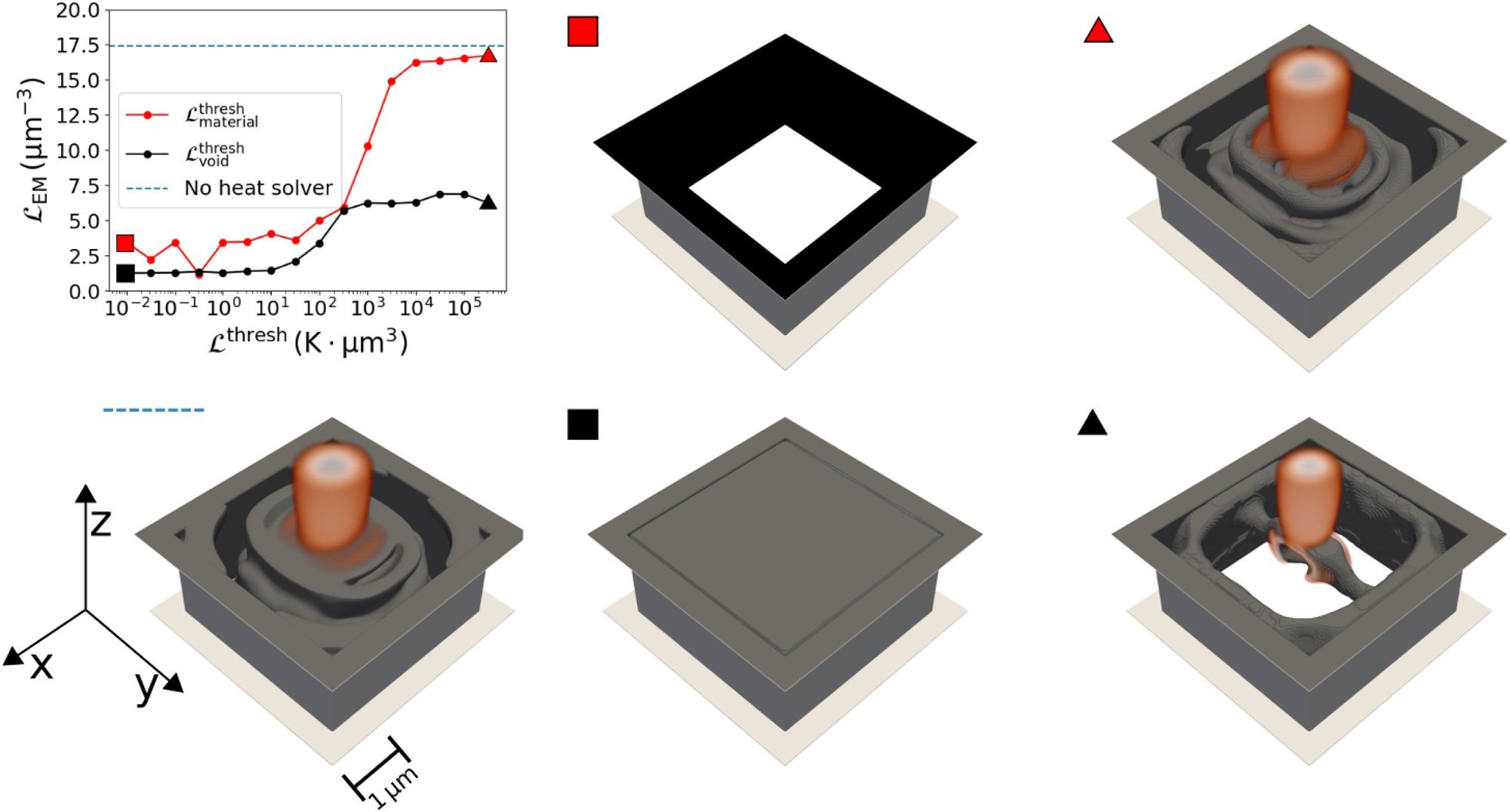
Different focusing devices designed with structural integrity. A parameter sweep is done by varying the threshold value for
In addition, Figure 2 shows various focusing devices where different values of
When looking into the results, we observe that if we choose the threshold value too small, the optimization process ends up in structures with ρ = 0 or ρ = 1 everywhere in the design region. This can be seen clearly in the exemplary devices with the red and black squares, where the optimized structure consists of only a void (red square) or only material (black square). This happens because normalizing to a tiny threshold value results in a thermal objective function that has a much higher value than the electromagnetic objective function by orders of magnitude. Since this happens in the linear regime of the softplus function, the gradient will also point towards a solution which optimizes the thermal objective over the electromagnetic objective. For example, when
Increasing the threshold leads to non-trivial structures which can function as proper focusing devices. Interestingly, it seems to be possible to increase the threshold value for either
In contrast, when considering only
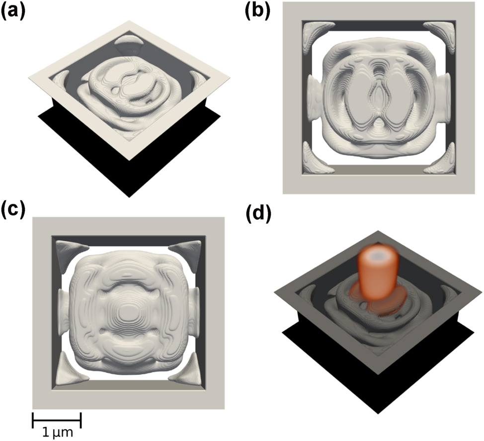
Best performing focusing device with enforced structural integrity, shown from different angles: Tilted (a), top view (b), and side view (c). The electric field distribution |E x | is shown in (d).
3.2 Waveguide coupler
The second design is a waveguide coupler. We consider two incoming waveguides for two different wavelengths λ 1 = 700 nm and λ 2 = 600 nm. The waveguides are made from a polymer characterized by a permittivity of ɛ r = 2.25. Each waveguide couples to an outgoing waveguide rotated by 90°. We place our heat sinks for the material at the waveguide ports, which is where we are certain that material is required for the optical performance. The heat sinks for the void are placed on the boundaries of the design domain except where the waveguides are. Our design region is defined by a cube with sidelength 2 μm, resulting in around half a million parameters for our chosen resolution. The full simulation domain has a size of 3 μm × 3 μm × 6 μm with the design region at its center. We use PMLs with width 0.5 μm. As a figure of merit, we choose to maximize the intensity of each field in their respective target waveguides
where
While the optimization that exclusively optimizes the electromagnetic response already favors structures that mostly possess structural integrity, the final designs may still contain free-floating artifacts and cavities. As with the focusing device, we sweep through both
The results of the parameter sweep can be seen in Figure 4. As with the focusing device, choosing the value for
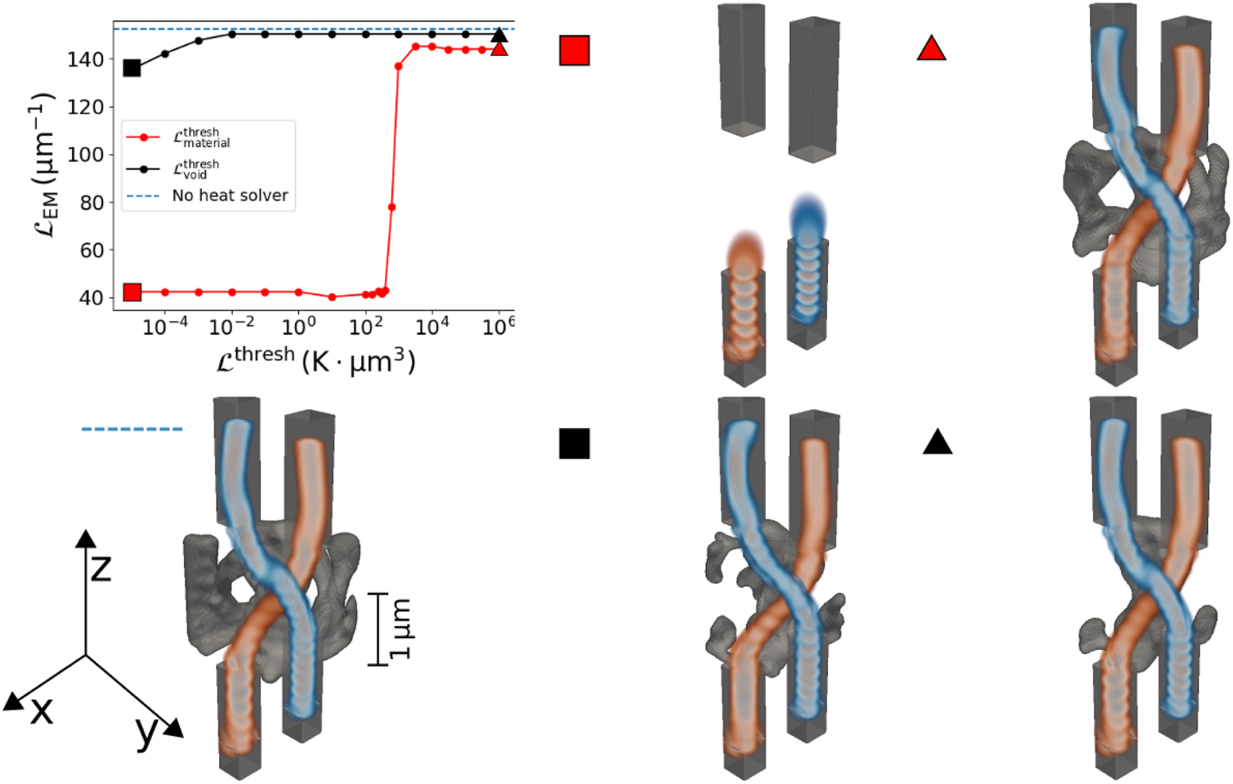
Different waveguide couplers designed with structural integrity. A parameter sweep is done by varying the threshold value for
The behavior is different when changing

Best performing waveguide crossings with enforced structural integrity, shown from different angles: Tilted (a), top view (b), and side view (c). The electric field distributions
Interestingly, both with and without the auxiliary heat solver, we find solutions that are not just two waveguides connecting the waveguide ports. Instead, we get structures with additional features. These additional features help to guide the light through the curved waveguides by catching the field which is propagating outside of the waveguides [56]. This leads to an increased performance, as even the tail end of the electromagnetic waves can be captured. Once we enforce structural integrity using our heat solver, we favor solutions with less material. The resulting less bulky structures still retain some of the additional features which catch the evanescent field outside the central waveguides, which seemingly still help to improve the performance of our waveguides. This phenomenon is similar to additional features appearing in 2D waveguide bends [50], [57], where resonator-like structures appear to improve the performance of the waveguide bend.
4 Discussion
This work introduces a robust methodology to ensure the structural integrity of 3D-printed nanophotonic devices through the integration of an auxiliary heat-diffusion solver within a gradient-based topology optimization framework. Our approach not only prevents disconnected or structurally unstable designs but also preserves the desired optical functionalities with minimal performance trade-offs.
By leveraging the heat-diffusion solver as a fictitious physics-based soft-constraint, we effectively enforce connectivity in both material and void domains. The use of renormalised figures of merit and the softplus function ensures that thermal optimisation ceases once structural integrity is achieved, allowing the optimizer to focus on the optical performance. In combination with the iterative binarization strategy, our approach results in designs that are directly fabricable, offering a streamlined pipeline for 3D nanoprinting applications.
The proposed framework was demonstrated through the design of two devices – a focusing element and a waveguide crossing. These case studies validate the effectiveness of our method in achieving structurally robust and optically performant devices. In both cases, the devices with structural integrity performed only marginally worse than those optimized for their optical performance only.
This study lays the foundation for a broader application of physics-based constraints in the design of complex 3D nanostructures. Future work could explore extensions of this methodology to include additional auxiliary (or indeed real) physical constraints. Further investigation into adaptive weighting schemes and thresholding strategies could also enhance the robustness and versatility of the optimization process. By addressing the longstanding challenge of structural integrity in 3D nanophotonic design, this work represents a significant step forward in enabling practical, high-performance devices for real-world applications.
Funding source: Alexander von Humboldt-Stiftung
Funding source: Deutsche Forschungsgemeinschaft
Award Identifier / Grant number: 390761711
Funding source: Carl-Zeiss-Stiftung
Acknowledgement
This work was performed on the HoreKa supercomputer funded by the Ministry of Science, Research and the Arts Baden-Württemberg and by the Federal Ministry of Education and Research.
-
Research funding: OK and CR acknowledge support from the German Research Foundation within the Excellence Cluster 3D Matter Made to Order (EXC 2082/1 under project number 390761711) and by the Carl Zeiss Foundation. TJS acknowledges funding from the Alexander von Humboldt Foundation.
-
Author contributions: All authors have accepted responsibility for the entire content of this manuscript and consented to its submission to the journal, reviewed all the results and approved the final version of the manuscript. CR, TJS and YA conceived the idea and surpervised the research. RNH has done initial investigations for 2D, OK wrote the code and designed the devices in 3D. OK wrote the manuscript. CR and TJS revised the paper.
-
Conflict of interest: Authors state no conflict of interest.
-
Data availability: The code to reproduce the datasets analyzed during the current study are available in the GitHub repository, https://github.com/OlloKuster/Structural_Integrity_3D/tree/main.
References
[1] J. Fischer and M. Wegener, “Three-dimensional optical laser lithography beyond the diffraction limit,” Laser Photonics Rev., vol. 7, no. 1, pp. 22–44, 2013, https://doi.org/10.1002/lpor.201100046.Suche in Google Scholar
[2] C. Barner-Kowollik, et al.., “3D laser micro- and nanoprinting: challenges for chemistry,” Angew. Chem., Int. Ed., vol. 56, no. 50, pp. 15828–15845, 2017, https://doi.org/10.1002/anie.201704695.Suche in Google Scholar PubMed
[3] V. Hahn, et al.., “Rapid assembly of small materials building blocks (voxels) into large functional 3d metamaterials,” Adv. Funct. Mater., vol. 30, no. 26, p. 1907795, 2020, https://doi.org/10.1002/adfm.201907795.Suche in Google Scholar
[4] P. Kiefer, H. Vincent, S. Kalt, Q. Sun, Y. M. Eggeler, and M. Wegener, “A multi-photon (7×7)-focus 3D laser printer based on a 3D-printed diffractive optical element and a 3D-printed multi-lens array,” Light: Adva. Manuf., vol. 4, no. 1, pp. 28–41, 2024.10.37188/lam.2024.003Suche in Google Scholar
[5] P. Somers, A. Münchinger, S. Maruo, C. Moser, X. Xu, and M. Wegener, “The physics of 3D printing with light,” Nat. Rev. Phys., vol. 6, no. 2, pp. 99–113, 2024.10.1038/s42254-023-00671-3Suche in Google Scholar
[6] H. Gehring, et al.., “Low-loss fiber-to-chip couplers with ultrawide optical bandwidth,” APL Photonics, vol. 4, no. 1, p. 010801, 2019, https://doi.org/10.1063/1.5064401.Suche in Google Scholar
[7] L. Siegle, D. Xie, C. A. Richards, P. V. Braun, and H. Giessen, “Diffractive microoptics in porous silicon oxide by grayscale lithography,” Opt. Express, vol. 32, no. 20, pp. 35678–35688, 2024, https://doi.org/10.1364/oe.538142.Suche in Google Scholar
[8] P. Ruchka, et al.., “3D-printed micro-axicon enables extended depth-of-focus intravascular optical coherence tomography in vivo,” Advanced Photonics, vol. 7, no. 2, 2025.10.1117/1.AP.7.2.026003Suche in Google Scholar
[9] M. D. Schmid, A. Toulouse, S. Thiele, M. Simon, A. M. Herkommer, and H. Giessen, “3D direct laser writing of highly absorptive photoresist for miniature optical apertures,” Adv. Funct. Mater., vol. 33, no. 39, p. 2211159, 2023, https://doi.org/10.1002/adfm.202211159.Suche in Google Scholar
[10] S. Papamakarios, I Katsantonis, M Kafesaki, K. L. Tsakmakidis, and M Farsari, “Cross-shaped resonators for BICs in mid-IR fabricated using multiphoton lithography,” in 2024 Eighteenth International Congress on Artificial Materials for Novel Wave Phenomena (Metamaterials), Crete, Greece, IEEE, 2024, pp. 1–3.10.1109/Metamaterials62190.2024.10703218Suche in Google Scholar
[11] O Tsilipakos, G Perrakis, M Farsari, and M Kafesaki, “Polymeric optical metasurfaces by two-photon lithography: practical designs for beam steering,” in 2024 Eighteenth International Congress on Artificial Materials for Novel Wave Phenomena (Metamaterials), Crete, Greece, IEEE, 2024, pp. 1–3.10.1109/Metamaterials62190.2024.10703264Suche in Google Scholar
[12] S. Papamakarios, et al.., “Cactus-like metamaterial structures for electromagnetically induced transparency at thz frequencies,” ACS Photonics, vol. 12, no. 1, 2024. https://doi.org/10.1021/acsphotonics.4c01179.Suche in Google Scholar PubMed PubMed Central
[13] D. Pereira, M. S. Ferreira, M. Zeisberger, and M. A. Schmidt, “Spatially controlled phase modulation - selective higher-order mode excitation in 3D nanoprinted on-Chip hollow-core waveguides,” ACS Photonics, vol. 11, no. 8, pp. 3178–3186, 2024, https://doi.org/10.1021/acsphotonics.4c00524.Suche in Google Scholar
[14] J. Bauer, C. Crook, and T. Baldacchini, “A sinterless, low-temperature route to 3D print nanoscale optical-grade glass,” Science, vol. 380, no. 6648, pp. 960–966, 2023, https://doi.org/10.1126/science.abq3037.Suche in Google Scholar PubMed
[15] Y. Dana, et al.., “Free-standing microscale photonic lantern spatial mode (De-) multiplexer fabricated using 3D nanoprinting,” Light: Sci. Appl., vol. 13, no. 1, p. 126, 2024, https://doi.org/10.1038/s41377-024-01466-6.Suche in Google Scholar PubMed PubMed Central
[16] S.-F. Liu, Z.-W. Hou, L. Lin, Z. Li, and H.-B. Sun, “3D laser nanoprinting of functional materials,” Adv. Funct. Mater., vol. 33, no. 39, p. 2211280, 2023, https://doi.org/10.1002/adfm.202211280.Suche in Google Scholar
[17] T. J. Sturges, et al.., “Inverse-designed 3D laser nanoprinted phase masks to extend the depth of field of imaging systems,” ACS Photonics, vol. 11, no. 9, pp. 3765–3773, 2024, https://doi.org/10.1021/acsphotonics.4c00953.Suche in Google Scholar
[18] C. Su, et al.., “Ring-in-ring beam shaping based on a 3D nanoprinted microlens on fiber tip,” in 2024 14th International Symposium on Communication Systems, Networks and Digital Signal Processing (CSNDSP), Rome, Italy, IEEE/IET, 2024, pp. 351–353.10.1109/CSNDSP60683.2024.10636389Suche in Google Scholar
[19] P. Mainik, C. A. Spiegel, and E. Blasco, “Recent advances in multi-photon 3D laser printing: active materials and applications,” Adv. Mater., vol. 36, no. 11, p. 2310100, 2024, https://doi.org/10.1002/adma.202310100.Suche in Google Scholar PubMed
[20] J. Bürger, J. Kim, T. Weiss, S. A. Maier, and M. A. Schmidt, “On-chip twisted hollow-core light cages: enhancing planar photonics with 3D nanoprinting,” Arxiv Preprint, 2024.Suche in Google Scholar
[21] H. Wang, et al.., “Two-photon polymerization lithography for imaging optics,” Int. J. Extreme Manuf., vol. 6, no. 4, p. 042002, 2024, https://doi.org/10.1088/2631-7990/ad35fe.Suche in Google Scholar
[22] G. C. Marques, et al.., “Fully printed electrolyte-gated transistor formed in a 3D polymer reservoir with laser printed drain/source electrodes,” Adv. Mater. Technol., vol. 8, no. 22, p. 2300893, 2023, https://doi.org/10.1002/admt.202300893.Suche in Google Scholar
[23] J. Weinacker, et al.., “Multi-photon 3d laser micro-printed plastic scintillators for applications in low-energy particle physics,” Adv. Funct. Mater., vol. 35, no. 2, p. 2413215, 2024. https://doi.org/10.1002/adfm.202413215.Suche in Google Scholar
[24] R. E. Christiansen and O. Sigmund, “Inverse design in photonics by topology optimization: tutorial,” J. Opt. Soc. Am. B, vol. 38, no. 2, p. 496, 2021, https://doi.org/10.1364/josab.406048.Suche in Google Scholar
[25] S. Molesky, Z. Lin, A. Y. Piggott, W. Jin, J. Vucković, and A. W. Rodriguez, “Inverse design in nanophotonics,” Nat. Photonics, vol. 12, no. 11, pp. 659–670, 2018, https://doi.org/10.1038/s41566-018-0246-9.Suche in Google Scholar
[26] J. Noh, T. Badloe, C. Lee, J. Yun, S. So, and J. Rho, “Inverse design meets nanophotonics: from computational optimization to artificial neural network,” Intel. Nanotechnol., pp. 3–32, 2023, https://doi.org/10.1016/b978-0-323-85796-3.00001-9.Suche in Google Scholar
[27] S. So, T. Badloe, J. Noh, J. Bravo-Abad, and J. Rho, “Deep learning enabled inverse design in nanophotonics,” Nanophotonics, vol. 9, no. 5, pp. 1041–1057, 2020, https://doi.org/10.1515/nanoph-2019-0474.Suche in Google Scholar
[28] P. R Wiecha, A. Arbouet, C. Girard, and O. L Muskens, “Deep learning in nano-photonics: inverse design and beyond,” Photonics Res., vol. 9, no. 5, pp. B182–B200, 2021, https://doi.org/10.1364/prj.415960.Suche in Google Scholar
[29] T. W. Radford, P. R. Wiecha, A. Politi, I. Zeimpekis, and O. L. Muskens, “Inverse design of unitary transmission matrices in silicon photonic coupled waveguide arrays using a neural adjoint model,” ACS Photonics, vol. 12, no. 3, 2025.10.1021/acsphotonics.4c02081Suche in Google Scholar PubMed PubMed Central
[30] D. Peng, K. Sun, O. L. Muskens, C. H. de Groot, and R. Huang, “Inverse design of a vanadium dioxide based dynamic structural color via conditional generative adversarial networks,” Opt. Mater. Express, vol. 12, no. 10, pp. 3970–3981, 2022, https://doi.org/10.1364/ome.467967.Suche in Google Scholar
[31] D. Lee, W. Chen, L. Wang, Y.-C. Chan, and W. Chen, “Data-driven design for metamaterials and multiscale systems: a review,” Adv. Mater., vol. 36, no. 8, p. 2305254, 2024, https://doi.org/10.1002/adma.202305254.Suche in Google Scholar PubMed
[32] I. Tanriover, D. Lee, W. Chen, and K. Aydin, “Deep generative modeling and inverse design of manufacturable free-form dielectric metasurfaces,” ACS Photonics, vol. 10, no. 4, pp. 875–883, 2023.10.1021/acsphotonics.2c01006Suche in Google Scholar
[33] J. S. Jensen and O. Sigmund, “Topology optimization for nano-photonics,” Laser Photonics Rev., vol. 5, no. 2, pp. 308–321, 2011, https://doi.org/10.1002/lpor.201000014.Suche in Google Scholar
[34] M. P. Bendsøe and O. Sigmund, “Bibliographical notes,” in Topology Optimization: Theory, Methods, and Applications, M. P. Bendsøe, and O. Sigmund, Eds., Berlin, Heidelberg, Springer, 2004, pp. 305–318.10.1007/978-3-662-05086-6_6Suche in Google Scholar
[35] N. V Sapra, et al.., “Inverse design and demonstration of broadband grating couplers,” IEEE J. Sel. Top. Quantum Electron., vol. 25, no. 3, pp. 1–7, 2019, https://doi.org/10.1109/jstqe.2019.2891402.Suche in Google Scholar
[36] N. Murai, Y. Noguchi, K. Matsushima, and T. Yamada, “Multiscale topology optimization of electromagnetic metamaterials using a high-contrast homogenization method,” Compu. Methods Appl. Mech. Eng., vol. 403, p. 115728, 2023, https://doi.org/10.1016/j.cma.2022.115728.Suche in Google Scholar
[37] A. Y. Piggott, J. Lu, K. G. Lagoudakis, J. Petykiewicz, T. M. Babinec, and J. Vučković, “Inverse design and demonstration of a compact and broadband on-chip wavelength demultiplexer,” Nat. Photonics, vol. 9, no. 6, pp. 374–377, 2015, https://doi.org/10.1038/nphoton.2015.69.Suche in Google Scholar
[38] A. Nanda, M. Kues, and A. C. Lesina, “Exploring the fundamental limits of integrated beam splitters with arbitrary phase via topology optimization,” Opt. Lett., vol. 49, no. 5, pp. 1125–1128, 2024, https://doi.org/10.1364/ol.512100.Suche in Google Scholar
[39] E. Hassan and A. C. Lesina, “Topology optimization of dispersive plasmonic nanostructures in the time-domain,” Opt. Express, vol. 30, no. 11, pp. 19557–19572, 2022, https://doi.org/10.1364/oe.458080.Suche in Google Scholar PubMed
[40] J. Gedeon, I. Allayarov, A. C. Lesina, and E. Hassan, “Time-domain topology optimization of power dissipation in dispersive dielectric and plasmonic nanostructures,” IEEE Trans. Antennas Propag., vol. 10, no. 11, 2025. https://doi.org/10.1109/tap.2024.3517156.Suche in Google Scholar
[41] V. Igoshin, A. Kokhanovskiy, and M. Petrov, “Inverse design of mie resonators with minimal backscattering,” Optics Letters, vol. 50, no. 5, 2025.10.1364/OL.552002Suche in Google Scholar PubMed
[42] V. D. Igoshin, A. Y. Kokhanovskiy, and M. I. Petrov, “Inverse design of stacked cylinders scatterers by evolutionary optimization,” in 2024 Photonics & Electromagnetics Research Symposium (PIERS), Chengdu, China, IEEE, 2024, pp. 1–5.10.1109/PIERS62282.2024.10618079Suche in Google Scholar
[43] W. Jin, S. Molesky, Z. Lin, K.-M. C Fu, and A. W Rodriguez, “Inverse design of compact multimode cavity couplers,” Optics express, vol. 26, no. 20, pp. 26713–26721, 2018, https://doi.org/10.1364/oe.26.026713.Suche in Google Scholar
[44] Y. Augenstein and C. Rockstuhl, “Inverse design of nanophotonic devices with structural integrity,” ACS Photonics, vol. 7, no. 8, pp. 2190–2196, 2020, https://doi.org/10.1021/acsphotonics.0c00699.Suche in Google Scholar
[45] B. M. de Aguirre Jokisch, R. E. Christiansen, and O. Sigmund, “Engineering optical forces through Maxwell stress tensor inverse design,” Journal of the Optical Society of America B, vol. 42, no. 4, 2025.10.1364/JOSAB.546272Suche in Google Scholar
[46] B. M. de Aguirre Jokisch, R. E. Christiansen, and O. Sigmund, “Topology optimization framework for designing efficient thermo-optical phase shifters,” J. Opt. Soc. Am. B, vol. 41, no. 2, pp. A18–A31, 2024, https://doi.org/10.1364/josab.499979.Suche in Google Scholar
[47] R. E Christiansen, “Inverse design of optical mode converters by topology optimization: tutorial,” J. Opt., vol. 25, no. 8, p. 083501, 2023, https://doi.org/10.1088/2040-8986/acdbdd.Suche in Google Scholar
[48] Q. Li, W. Chen, S. Liu, and L. Tong, “Structural topology optimization considering connectivity constraint,” Struct. Multidiscip. Optim., vol. 54, no. 4, pp. 971–984, 2016, https://doi.org/10.1007/s00158-016-1459-5.Suche in Google Scholar
[49] J. D. Fischbach, “Jan-david-fischbach/jaxwell,” 2024. Available at: https://github.com/jan-david-fischbach/jaxwell.Suche in Google Scholar
[50] M. F. Schubert, A. K. C. Cheung, I. A. D. Williamson, A. Spyra, and D. H. Alexander, “Inverse design of photonic devices with strict foundry fabrication constraints,” ACS Photonics, vol. 9, no. 7, pp. 2327–2336, 2022, https://doi.org/10.1021/acsphotonics.2c00313.Suche in Google Scholar
[51] C. M. Lalau-Keraly, S. Bhargava, O. D. Miller, and E. Yablonovitch, “Adjoint shape optimization applied to electromagnetic design,” Opt. Express, vol. 21, no. 18, p. 21693, 2013, https://doi.org/10.1364/oe.21.021693.Suche in Google Scholar PubMed
[52] M. P. Bendsøe, “Optimal shape design as a material distribution problem,” Struct. optim., vol. 1, no. 4, pp. 193–202, 1989, https://doi.org/10.1007/bf01650949.Suche in Google Scholar
[53] O. Sigmund and K. Maute, “Topology optimization approaches,” Struct. Multidiscip. Optim., vol. 48, no. 6, pp. 1031–1055, 2013, https://doi.org/10.1007/s00158-013-0978-6.Suche in Google Scholar
[54] M. Zhou, B. S. Lazarov, F. Wang, and O. Sigmund, “Minimum length scale in topology optimization by geometric constraints,” Compu. Methods Appl. Mech. Eng., vol. 293, pp. 266–282, 2015, https://doi.org/10.1016/j.cma.2015.05.003.Suche in Google Scholar
[55] F. Wang, B. Stefanov Lazarov, and O. Sigmund, “On projection methods, convergence and robust formulations in topology optimization,” Struct. Multidiscip. Optim., vol. 43, no. 6, pp. 767–784, 2011, https://doi.org/10.1007/s00158-010-0602-y.Suche in Google Scholar
[56] M. Paszkiewicz-Idzik, M. Sukhova, W. Dörfler, and C. Rockstuhl, “Optimizing the trajectories of freeform waveguides using a modal theory,” in Computational Optics, vol. PC13023, D. G. Smith and A. Erdmann, Eds., San Diego, USA, SPIE/International Society for Optics and Photonics, 2024, p. PC1302305.10.1117/12.3014421Suche in Google Scholar
[57] S. Irfan, J.-Y. Kim, and H. Kurt, “Ultra-compact and efficient photonic waveguide bends with different configurations designed by topology optimization,” Sci. Rep., vol. 14, no. 1, p. 6453, 2024, https://doi.org/10.1038/s41598-024-53881-9.Suche in Google Scholar PubMed PubMed Central
Supplementary Material
This article contains supplementary material (https://doi.org/10.1515/nanoph-2025-0067).
© 2025 the author(s), published by De Gruyter, Berlin/Boston
This work is licensed under the Creative Commons Attribution 4.0 International License.
Artikel in diesem Heft
- Frontmatter
- Review
- Anisotropic metamaterials for scalable photonic integrated circuits: a review on subwavelength gratings for high-density integration
- Research Articles
- Disorder robust, ultra-low power, continuous-wave four-wave mixing in a topological waveguide
- Continuously adjustable hollow beam for ultrafast laser fabrication of size-controllable nanoparticles
- Generation of fast photoelectrons in strong-field emission from metal nanoparticles
- Interband plasmonic nanoresonators for enhanced thermoelectric photodetection
- Low-cost large-area 100 GHz intelligent reflective surface: electrically column control of screen-printable high phase changing ratio vanadium dioxides
- Metasurface-enabled optical encryption and steganography with enhanced information security
- Radial rotation of cell-pair under beam mode coupling effect of microcavity cascaded single fiber optical tweezers
- Inverse design of 3D nanophotonic devices with structural integrity using auxiliary thermal solvers